EP0803949A2 - Diodenlaservorrichtung angeordnet auf Halbleiterstäben - Google Patents
Diodenlaservorrichtung angeordnet auf Halbleiterstäben Download PDFInfo
- Publication number
- EP0803949A2 EP0803949A2 EP97400861A EP97400861A EP0803949A2 EP 0803949 A2 EP0803949 A2 EP 0803949A2 EP 97400861 A EP97400861 A EP 97400861A EP 97400861 A EP97400861 A EP 97400861A EP 0803949 A2 EP0803949 A2 EP 0803949A2
- Authority
- EP
- European Patent Office
- Prior art keywords
- semiconductor
- groove
- ribs
- grooves
- bars
- Prior art date
- Legal status (The legal status is an assumption and is not a legal conclusion. Google has not performed a legal analysis and makes no representation as to the accuracy of the status listed.)
- Granted
Links
Images

Classifications
-
- H—ELECTRICITY
- H01—ELECTRIC ELEMENTS
- H01S—DEVICES USING THE PROCESS OF LIGHT AMPLIFICATION BY STIMULATED EMISSION OF RADIATION [LASER] TO AMPLIFY OR GENERATE LIGHT; DEVICES USING STIMULATED EMISSION OF ELECTROMAGNETIC RADIATION IN WAVE RANGES OTHER THAN OPTICAL
- H01S5/00—Semiconductor lasers
- H01S5/02—Structural details or components not essential to laser action
- H01S5/022—Mountings; Housings
- H01S5/023—Mount members, e.g. sub-mount members
- H01S5/02315—Support members, e.g. bases or carriers
-
- H—ELECTRICITY
- H01—ELECTRIC ELEMENTS
- H01S—DEVICES USING THE PROCESS OF LIGHT AMPLIFICATION BY STIMULATED EMISSION OF RADIATION [LASER] TO AMPLIFY OR GENERATE LIGHT; DEVICES USING STIMULATED EMISSION OF ELECTROMAGNETIC RADIATION IN WAVE RANGES OTHER THAN OPTICAL
- H01S5/00—Semiconductor lasers
- H01S5/02—Structural details or components not essential to laser action
- H01S5/022—Mountings; Housings
- H01S5/0233—Mounting configuration of laser chips
-
- H—ELECTRICITY
- H01—ELECTRIC ELEMENTS
- H01S—DEVICES USING THE PROCESS OF LIGHT AMPLIFICATION BY STIMULATED EMISSION OF RADIATION [LASER] TO AMPLIFY OR GENERATE LIGHT; DEVICES USING STIMULATED EMISSION OF ELECTROMAGNETIC RADIATION IN WAVE RANGES OTHER THAN OPTICAL
- H01S5/00—Semiconductor lasers
- H01S5/02—Structural details or components not essential to laser action
- H01S5/022—Mountings; Housings
- H01S5/0235—Method for mounting laser chips
-
- H—ELECTRICITY
- H01—ELECTRIC ELEMENTS
- H01S—DEVICES USING THE PROCESS OF LIGHT AMPLIFICATION BY STIMULATED EMISSION OF RADIATION [LASER] TO AMPLIFY OR GENERATE LIGHT; DEVICES USING STIMULATED EMISSION OF ELECTROMAGNETIC RADIATION IN WAVE RANGES OTHER THAN OPTICAL
- H01S5/00—Semiconductor lasers
- H01S5/02—Structural details or components not essential to laser action
- H01S5/024—Arrangements for thermal management
-
- H—ELECTRICITY
- H01—ELECTRIC ELEMENTS
- H01S—DEVICES USING THE PROCESS OF LIGHT AMPLIFICATION BY STIMULATED EMISSION OF RADIATION [LASER] TO AMPLIFY OR GENERATE LIGHT; DEVICES USING STIMULATED EMISSION OF ELECTROMAGNETIC RADIATION IN WAVE RANGES OTHER THAN OPTICAL
- H01S5/00—Semiconductor lasers
- H01S5/04—Processes or apparatus for excitation, e.g. pumping, e.g. by electron beams
- H01S5/042—Electrical excitation ; Circuits therefor
-
- H—ELECTRICITY
- H01—ELECTRIC ELEMENTS
- H01S—DEVICES USING THE PROCESS OF LIGHT AMPLIFICATION BY STIMULATED EMISSION OF RADIATION [LASER] TO AMPLIFY OR GENERATE LIGHT; DEVICES USING STIMULATED EMISSION OF ELECTROMAGNETIC RADIATION IN WAVE RANGES OTHER THAN OPTICAL
- H01S5/00—Semiconductor lasers
- H01S5/40—Arrangement of two or more semiconductor lasers, not provided for in groups H01S5/02 - H01S5/30
- H01S5/4025—Array arrangements, e.g. constituted by discrete laser diodes or laser bar
-
- H—ELECTRICITY
- H01—ELECTRIC ELEMENTS
- H01S—DEVICES USING THE PROCESS OF LIGHT AMPLIFICATION BY STIMULATED EMISSION OF RADIATION [LASER] TO AMPLIFY OR GENERATE LIGHT; DEVICES USING STIMULATED EMISSION OF ELECTROMAGNETIC RADIATION IN WAVE RANGES OTHER THAN OPTICAL
- H01S5/00—Semiconductor lasers
- H01S5/40—Arrangement of two or more semiconductor lasers, not provided for in groups H01S5/02 - H01S5/30
- H01S5/42—Arrays of surface emitting lasers
-
- H—ELECTRICITY
- H01—ELECTRIC ELEMENTS
- H01S—DEVICES USING THE PROCESS OF LIGHT AMPLIFICATION BY STIMULATED EMISSION OF RADIATION [LASER] TO AMPLIFY OR GENERATE LIGHT; DEVICES USING STIMULATED EMISSION OF ELECTROMAGNETIC RADIATION IN WAVE RANGES OTHER THAN OPTICAL
- H01S5/00—Semiconductor lasers
- H01S5/02—Structural details or components not essential to laser action
- H01S5/022—Mountings; Housings
- H01S5/0233—Mounting configuration of laser chips
- H01S5/02345—Wire-bonding
-
- H—ELECTRICITY
- H01—ELECTRIC ELEMENTS
- H01S—DEVICES USING THE PROCESS OF LIGHT AMPLIFICATION BY STIMULATED EMISSION OF RADIATION [LASER] TO AMPLIFY OR GENERATE LIGHT; DEVICES USING STIMULATED EMISSION OF ELECTROMAGNETIC RADIATION IN WAVE RANGES OTHER THAN OPTICAL
- H01S5/00—Semiconductor lasers
- H01S5/02—Structural details or components not essential to laser action
- H01S5/024—Arrangements for thermal management
- H01S5/02407—Active cooling, e.g. the laser temperature is controlled by a thermo-electric cooler or water cooling
- H01S5/02423—Liquid cooling, e.g. a liquid cools a mount of the laser
-
- H—ELECTRICITY
- H01—ELECTRIC ELEMENTS
- H01S—DEVICES USING THE PROCESS OF LIGHT AMPLIFICATION BY STIMULATED EMISSION OF RADIATION [LASER] TO AMPLIFY OR GENERATE LIGHT; DEVICES USING STIMULATED EMISSION OF ELECTROMAGNETIC RADIATION IN WAVE RANGES OTHER THAN OPTICAL
- H01S5/00—Semiconductor lasers
- H01S5/40—Arrangement of two or more semiconductor lasers, not provided for in groups H01S5/02 - H01S5/30
- H01S5/4018—Lasers electrically in series
-
- H—ELECTRICITY
- H01—ELECTRIC ELEMENTS
- H01S—DEVICES USING THE PROCESS OF LIGHT AMPLIFICATION BY STIMULATED EMISSION OF RADIATION [LASER] TO AMPLIFY OR GENERATE LIGHT; DEVICES USING STIMULATED EMISSION OF ELECTROMAGNETIC RADIATION IN WAVE RANGES OTHER THAN OPTICAL
- H01S5/00—Semiconductor lasers
- H01S5/40—Arrangement of two or more semiconductor lasers, not provided for in groups H01S5/02 - H01S5/30
- H01S5/4025—Array arrangements, e.g. constituted by discrete laser diodes or laser bar
- H01S5/4031—Edge-emitting structures
- H01S5/4037—Edge-emitting structures with active layers in more than one orientation
-
- H—ELECTRICITY
- H01—ELECTRIC ELEMENTS
- H01S—DEVICES USING THE PROCESS OF LIGHT AMPLIFICATION BY STIMULATED EMISSION OF RADIATION [LASER] TO AMPLIFY OR GENERATE LIGHT; DEVICES USING STIMULATED EMISSION OF ELECTROMAGNETIC RADIATION IN WAVE RANGES OTHER THAN OPTICAL
- H01S5/00—Semiconductor lasers
- H01S5/40—Arrangement of two or more semiconductor lasers, not provided for in groups H01S5/02 - H01S5/30
- H01S5/4025—Array arrangements, e.g. constituted by discrete laser diodes or laser bar
- H01S5/4031—Edge-emitting structures
- H01S5/4056—Edge-emitting structures emitting light in more than one direction
Definitions
- diode laser devices are numerous, such as for example pumping solid-state lasers (see American patent N ° 4,847,851), fiber optic connections, laser treatment of materials, medicine, etc.
- the diode laser devices currently known and described in the above prior art are essentially of two types.
- the semiconductor bars are welded flat on one face of the heat diffusing substrate and this face is machined to present, between two adjacent semiconductor bars, mirrors capable of reflecting the radiation emitted by said diodes. , opposite to said face.
- the heat is efficiently extracted of said diodes, so that they operate reliably.
- a system of parallel ribs and grooves with rectangular sections is provided in one face of the heat-diffusing substrate, said grooves forming housings in which said semiconductor bars are arranged longitudinally in song.
- the object of the present invention is to remedy these drawbacks by increasing the density and uniformity of the radiation of a diode laser device. It makes it possible to increase the heat exchanges between the strips and the heat diffusing substrate as well as the lifetime of said diodes, while simplifying the electrical connections of the semiconductor strips and making it possible to automate the production of said device and therefore to '' reduce manufacturing costs.
- each rib form a dihedral angle between them at least approximately equal to the divergence angle of said laser diodes, for example of the order of 60 °.
- the laser diodes are arranged in the vicinity of the cooling surface on the massive base of the triangular ribs, good heat dissipation is ensured from the junctions of the laser diodes.
- the light flux from said diodes thus arranged obliquely overlap, which increases the density and uniformity of the resulting radiation. A reasonable compromise is thus obtained with regard to the density of coverage of the surface of the diffusing substrate by the semiconductor bars.
- said system of ribs and parallel grooves is coated with a metallization film on which said semiconductor strips are fixed flat and said metallization film has interruption strips parallel to said ribs and grooves.
- interrupt strips are advantageously obtained by deliberate destruction of the metallization film, initially uniform, in particular places, for example directly above the tops of the ribs or directly below the bottoms of the grooves.
- a film of a conductive material is provided between said system of ribs and grooves and said metallization film. heat, but not electrically conductive.
- the two semiconductor bars of a groove are mounted in parallel and the parallel arrangements of the two bars of all the grooves are connected in series.
- connection diagram is simple and that the manufacture can be easily automated.
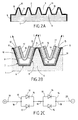
- Figure 1 shows, in perspective, the heat diffusing substrate of the diode laser device according to the present invention.
- Figures 2A, 2B and 2C illustrate a first embodiment of the diode laser device of the invention.
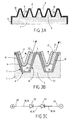
- Figures 3A, 3B and 3C illustrate a second embodiment of the diode laser device of the invention.
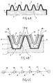
- FIGS. 4A, 4B and 4C illustrate a third embodiment of the diode laser device of the invention.
- the heat diffusing substrate 1 for the diode laser device of the invention represented in FIG. 1, consists of a block of generally parallelepiped shape in a material highly conductive of heat, but, preferably, little or not electrically conductive, such as diamond, silicon carbide, beryllium oxide, etc. It is advantageous that, in addition, it is made porous or provided with micro-channels, by any known process.
- the faces of the substrate 1 can be polished until obtaining roughness at most equal to 3 nanometers.
- the substrate is carried by a cooling system, not shown.
- a system of ribs 2 and grooves 3 parallel said ribs being identical and equidistant.
- this system comprises five ribs 2 of at least approximately triangular section and four grooves 3 of at least approximately trapezoidal section, each groove 3 being defined by the space between two adjacent parallel ribs 2.
- Each rib 2 is connected to the substrate 1 by a wide base 4 and its apex 5, directed opposite to said substrate 1, can be cut.
- Each groove 3 opens opposite to said substrate 1 by widening from its bottom 6.
- Each rib 2 has two flat sides 7 and 8, oblique and convergent, forming between them a dihedral angle a .
- each groove 3 is delimited between the diverging flat sides 7 and 8 of two adjacent ribs 2.
- the part of the substrate 1 which carries the ribs 2 and the grooves 3 is coated with a film 9 of a material which is conductive of heat, but not conductive of the electricity, such as silicon carbide.
- the film 9 covers in particular the bottoms 6 of the grooves 3, as well as the top 5 and the sides 7 and 8 of the ribs 2. It can have a thickness of the order of 50 to 200 microns.
- the purpose of the film 9 is to further increase the smoothness of the substrate 1.
- the thermally conductive film 9 is covered by a metallization film 10, for example in chromium, titanium, nickel, gold, silver or a alloy of these metals.
- the metallization film 10 can have a thickness of the order of 50 to 200 microns.
- the metallization film 10 covers the film 9 directly above the bottoms 6 of the grooves 3 and of the sides 7 and 8 of the ribs 2, but is destroyed below the tops 5 of these.
- the film 10 is interrupted along strips 11 in which the film 9 appears.
- each of said grooves 3 are mounted two semiconductor bars carrying laser diodes .
- These semiconductor bars have the references 12 and 13 for one of the grooves 3 and the references 14 and 15 for the other of the said grooves.
- Each of the semiconductor bars 12 to 15 is assumed to be of type n and is fixed flat on the side of the substrate to the part of the metallization film 10 which covers either an oblique flank 7 or an oblique flank 8, for example by welding using a low melting temperature solder such as indium, tin or gold.
- each groove 3 a semiconductor strip 12 or 14 is carried by the corresponding oblique flank 7, while the other semiconductor strip 13 or 15 is carried by the associated oblique flank 8, so that the two strips semiconductor of a groove, 12 and 13 on the one hand and 14 and 15 on the other hand, are electrically connected to each other by their fixing faces, via the parts of the metallization film 10 covering the bottom 6 and the oblique sides 7 and 8.
- an electrically conductive strip 16 in the form of a V for example metallic (copper) and having a thickness of between 50 and 200 microns, connects electrically the faces of the corresponding semiconductor bars 12 and 13 or 14 and 15, opposite the fixing faces of the latter.
- a thermally and electrically conductive bonding layer 17 can be provided between the conductive strips 16 and the diodes 12 to 15.
- the semiconductor strip 12 is electrically mounted in parallel on the semiconductor strip 13, on the one hand by the metallization film 10 covering the corresponding groove 3 and on the other hand by the associated conductive strip 16.
- the semiconductor strip 14 is electrically mounted in parallel on the semiconductor strip 15, on the one hand by the metallization film 10 covering the corresponding groove 3 and on the other hand by the associated conductive strip 16.
- the parallel assemblies of the bars, 12 and 13 on the one hand and 14 and 15 on the other hand can moreover be connected in series by a conductor 18 connecting the strip 16 of the diodes 12 and 13 to the part of the film 10 associated diodes 14 and 15.
- a conductor 18 is shown in Figure 2C, but not in Figure 2B.
- a conductor 19 can connect the pole + of an electrical source to the film 10 of the first pair of strips in parallel, while a conductor 20 can connect the conductive strip 16 of the last pair of bars parallel to the pole - of said electrical source.
- the metallization film 10 covers the film 9 plumb with the vertices 5 and the oblique sides 7 and 8 of the ribs 2, but not plumb with the bottoms 6 of the grooves 3. Consequently, in correspondence with said bottoms 6, the film 10 is interrupted along the bands 21 in which the film 9 appears.
- each of said grooves 3 is mounted only a single semiconductor strip carrying laser diodes.
- this bar carries the reference 22 for one of the grooves 3 and the reference 23 for the adjacent groove 3.
- the semiconductor bars 22 and 23 are assumed to be of type n and each of them is fixed to the oblique face 8 of the groove 3 in which it is located, as has been described above with regard to the bars 13 and 15.
- each electrically conductive strip 16 in the form of a V electrically connects the face of the strip 22 or 23, opposite the fixing face of the latter, to the part of the metallization film 10 covering the oblique face. 7 corresponding.
- the two semiconductor bars 22 and 23 are mounted in series via the conductive strip 16 associated with the bar 23 and the part of the metallization film 10 covering the rib 2 separating said bars.
- each groove 3 comprises two semiconductor bars 26 and 27 or 28 and 29 respectively, mounted identically to the semiconductor bars 12 and 13, or 14 and 15 of Figure 2B.
- the semiconductor bars 26 and 28, mounted on the oblique faces 7, are of type n
- the semiconductor bars 27 and 29, mounted on the oblique faces 8, are of type p .
- the two bars 26 and 27, of opposite conduction types are mounted in series by the corresponding V-shaped conductive strip 16. It is the same for the two bars 28 and 29. Furthermore, the bars 27 and 28, also of opposite conduction types, are connected to each other in series by the part of the metallization film 10 covering the rib 2 separating the two adjacent grooves 3. As a result, as illustrated in FIG. 4C, the four semiconductor bars 26 to 29 are connected in series, due, on the one hand, to the alternation of their type of conduction and, on the other hand, electrical connections established alternately by the metallization film 10 and by the electrically conductive strips 16.
- the radiation of the diodes of the semiconductor bars has been represented by arrows L.
- the dihedral angle has oblique planar sides 7 and 8 of the ribs 2 is defined by the divergence of the radiation L of the laser diodes.
- this angle a By choosing the value of this angle a , it is possible to obtain maximum uniformity of the radiation at a certain distance from the device.
- the number of laser diode arrays can be increased or decreased per unit area of the substrate.
- the tops 5 of the ribs and the bottoms 6 of the grooves can be acute, flat or rounded. Their appearance is determined by the method of electrical connection of the laser diode arrays.
- the oblique sides 7 and 8 of the ribs 2 must have a width greater than that of a strip of laser diodes ( ⁇ 0.5 mm). Technologically it is convenient that it is greater than 0.8-1.0 mm. If the angle a is equal to 60 ° (typical value of the angle of divergence of the radiation of the laser diodes), then, over a length of 1 cm, it is possible to have up to 20 strips of laser diodes.
- the thickness of the metallization film 10 and of the connection strips 16 is chosen to be between 50 and 200 ⁇ m so that these can easily let currents pass up to 100 amperes for durations of 200 to 400 ⁇ s.
- the structure of the laser diode device according to the invention allows automatic production to be carried out using a template having the same profile as the laser diode arrays.
- the end of the laser diode arrays directed towards the bottom 6 of the grooves 3 is advantageously covered with a 100% reflective layer, so that the radiation is only directed outwards.
- the heat diffusing substrate 1 is fixed (for example by gluing) to a cooling system (not shown), for example of the type with fluid circulation.
- this substrate can have a porous or micro-channel structure through which a coolant can be passed.
Landscapes
- Physics & Mathematics (AREA)
- Condensed Matter Physics & Semiconductors (AREA)
- General Physics & Mathematics (AREA)
- Electromagnetism (AREA)
- Optics & Photonics (AREA)
- Semiconductor Lasers (AREA)
- Cooling Or The Like Of Semiconductors Or Solid State Devices (AREA)
Applications Claiming Priority (2)
| Application Number | Priority Date | Filing Date | Title |
|---|---|---|---|
| RU96108180 | 1996-04-23 | ||
| RU96108180A RU2130221C1 (ru) | 1996-04-23 | 1996-04-23 | Матрица лазерных диодов |
Publications (3)
| Publication Number | Publication Date |
|---|---|
| EP0803949A2 true EP0803949A2 (de) | 1997-10-29 |
| EP0803949A3 EP0803949A3 (de) | 1998-03-04 |
| EP0803949B1 EP0803949B1 (de) | 2001-09-05 |
Family
ID=20179823
Family Applications (1)
| Application Number | Title | Priority Date | Filing Date |
|---|---|---|---|
| EP97400861A Expired - Lifetime EP0803949B1 (de) | 1996-04-23 | 1997-04-17 | Diodenlaservorrichtung |
Country Status (5)
| Country | Link |
|---|---|
| US (1) | US5930279A (de) |
| EP (1) | EP0803949B1 (de) |
| JP (1) | JP3828237B2 (de) |
| DE (1) | DE69706468T2 (de) |
| RU (1) | RU2130221C1 (de) |
Cited By (2)
| Publication number | Priority date | Publication date | Assignee | Title |
|---|---|---|---|---|
| GB2477458A (en) * | 2009-06-09 | 2011-08-03 | Mitsubishi Electric Corp | Multi-wavelength semiconductor laser device |
| GB2470984B (en) * | 2009-06-09 | 2012-03-07 | Mitsubishi Electric Corp | Multi-wavelength semiconductor laser device |
Families Citing this family (28)
| Publication number | Priority date | Publication date | Assignee | Title |
|---|---|---|---|---|
| US6295307B1 (en) | 1997-10-14 | 2001-09-25 | Decade Products, Inc. | Laser diode assembly |
| US6266353B1 (en) * | 1999-07-30 | 2001-07-24 | The Regents Of The University Of California | Monolithic laser diode array with one metalized sidewall |
| US6647035B1 (en) * | 2000-10-17 | 2003-11-11 | The Regents Of The University Of California | Ruggedized microchannel-cooled laser diode array with self-aligned microlens |
| LT5257B (lt) | 2003-12-19 | 2005-08-25 | U�daroji akcin� bendrov� MGF "�viesos konversija" | Ryškį išsaugojantis lazerinių pluoštų formuotuvas |
| RU2281583C1 (ru) * | 2005-03-09 | 2006-08-10 | Александр Андреевич Петров | Светоизлучающее устройство |
| US8134163B2 (en) | 2008-08-11 | 2012-03-13 | Taiwan Semiconductor Manfacturing Co., Ltd. | Light-emitting diodes on concave texture substrate |
| US9293656B2 (en) * | 2012-11-02 | 2016-03-22 | Epistar Corporation | Light emitting device |
| US8716723B2 (en) * | 2008-08-18 | 2014-05-06 | Tsmc Solid State Lighting Ltd. | Reflective layer between light-emitting diodes |
| US8995485B2 (en) | 2009-02-17 | 2015-03-31 | Trilumina Corp. | High brightness pulsed VCSEL sources |
| US8995493B2 (en) | 2009-02-17 | 2015-03-31 | Trilumina Corp. | Microlenses for multibeam arrays of optoelectronic devices for high frequency operation |
| US10038304B2 (en) | 2009-02-17 | 2018-07-31 | Trilumina Corp. | Laser arrays for variable optical properties |
| US20130223846A1 (en) | 2009-02-17 | 2013-08-29 | Trilumina Corporation | High speed free-space optical communications |
| US10244181B2 (en) | 2009-02-17 | 2019-03-26 | Trilumina Corp. | Compact multi-zone infrared laser illuminator |
| CN102959811B (zh) * | 2009-12-19 | 2016-06-29 | 三流明公司 | 用于组合用于数字输出的激光器阵列的系统和方法 |
| US8979338B2 (en) | 2009-12-19 | 2015-03-17 | Trilumina Corp. | System for combining laser array outputs into a single beam carrying digital data |
| TWI446578B (zh) * | 2010-09-23 | 2014-07-21 | Epistar Corp | 發光元件及其製法 |
| US11095365B2 (en) | 2011-08-26 | 2021-08-17 | Lumentum Operations Llc | Wide-angle illuminator module |
| DE102012209266A1 (de) | 2012-06-01 | 2013-12-05 | Robert Bosch Gmbh | Schaltungsanordnung und Herstellungsverfahren hierfür |
| US9510478B2 (en) * | 2013-06-20 | 2016-11-29 | Honeywell International Inc. | Cooling device including etched lateral microchannels |
| JP2016081562A (ja) | 2014-10-09 | 2016-05-16 | ソニー株式会社 | 表示装置、表示装置の製造方法および電子機器 |
| CN105720478A (zh) * | 2016-04-26 | 2016-06-29 | 西安炬光科技股份有限公司 | 一种可替换芯片的传导冷却型半导体激光器及其制备方法 |
| US11025031B2 (en) | 2016-11-29 | 2021-06-01 | Leonardo Electronics Us Inc. | Dual junction fiber-coupled laser diode and related methods |
| US11406004B2 (en) | 2018-08-13 | 2022-08-02 | Leonardo Electronics Us Inc. | Use of metal-core printed circuit board (PCB) for generation of ultra-narrow, high-current pulse driver |
| US11056854B2 (en) | 2018-08-14 | 2021-07-06 | Leonardo Electronics Us Inc. | Laser assembly and related methods |
| US11296481B2 (en) | 2019-01-09 | 2022-04-05 | Leonardo Electronics Us Inc. | Divergence reshaping array |
| US11752571B1 (en) | 2019-06-07 | 2023-09-12 | Leonardo Electronics Us Inc. | Coherent beam coupler |
| EP3792683A1 (de) | 2019-09-16 | 2021-03-17 | Leonardo Electronics US Inc. | Hexagonaler homogenisator mit asymmetrischer eingangsintensität |
| CN111193179B (zh) * | 2020-03-06 | 2025-06-06 | 西安炬光科技股份有限公司 | 激光叠阵 |
Family Cites Families (11)
| Publication number | Priority date | Publication date | Assignee | Title |
|---|---|---|---|---|
| GB1597707A (en) * | 1978-03-08 | 1981-09-09 | Aei Semiconductors Ltd | Electronic component assemblies |
| JPS5885368U (ja) * | 1981-12-04 | 1983-06-09 | 沖電気工業株式会社 | レ−ザダイオ−ドアレイ装置 |
| US4847851A (en) * | 1988-05-19 | 1989-07-11 | University Of South Florida | Butt-coupled single transverse mode diode pumped laser |
| US4881237A (en) * | 1988-08-26 | 1989-11-14 | Massachusetts Institute Of Technology | Hybrid two-dimensional surface-emitting laser arrays |
| JPH0323688A (ja) * | 1989-06-21 | 1991-01-31 | Mitsubishi Electric Corp | 半導体レーザ装置の製造方法 |
| NL9000161A (nl) * | 1990-01-23 | 1991-08-16 | Koninkl Philips Electronics Nv | Halfgeleiderinrichting bevattende een drager en werkwijze voor het vervaardigen van de drager. |
| US5128951A (en) * | 1991-03-04 | 1992-07-07 | Karpinski Arthur A | Laser diode array and method of fabrication thereof |
| US5349210A (en) * | 1993-02-02 | 1994-09-20 | Motorola, Inc. | Optical reading head with angled array |
| JPH0851247A (ja) * | 1994-08-05 | 1996-02-20 | Mitsubishi Electric Corp | 集積型半導体レーザ装置の製造方法,及び集積型半導体レーザ装置 |
| US5898211A (en) * | 1996-04-30 | 1999-04-27 | Cutting Edge Optronics, Inc. | Laser diode package with heat sink |
| US5828683A (en) * | 1997-04-21 | 1998-10-27 | The Regents Of The University Of California | High density, optically corrected, micro-channel cooled, v-groove monolithic laser diode array |
-
1996
- 1996-04-23 RU RU96108180A patent/RU2130221C1/ru active
-
1997
- 1997-04-17 EP EP97400861A patent/EP0803949B1/de not_active Expired - Lifetime
- 1997-04-17 DE DE69706468T patent/DE69706468T2/de not_active Expired - Lifetime
- 1997-04-22 US US08/840,602 patent/US5930279A/en not_active Expired - Fee Related
- 1997-04-23 JP JP10613097A patent/JP3828237B2/ja not_active Expired - Fee Related
Cited By (5)
| Publication number | Priority date | Publication date | Assignee | Title |
|---|---|---|---|---|
| GB2477458A (en) * | 2009-06-09 | 2011-08-03 | Mitsubishi Electric Corp | Multi-wavelength semiconductor laser device |
| GB2470984B (en) * | 2009-06-09 | 2012-03-07 | Mitsubishi Electric Corp | Multi-wavelength semiconductor laser device |
| GB2477458B (en) * | 2009-06-09 | 2012-03-07 | Mitsubishi Electric Corp | Multi-wavelength semiconductor laser device |
| US8351482B2 (en) | 2009-06-09 | 2013-01-08 | Mitsubishi Electric Corporation | Multi-wavelength semiconductor laser device |
| US8687668B2 (en) | 2009-06-09 | 2014-04-01 | Mitsubishi Electric Corporation | Multi-wavelength semiconductor laser device |
Also Published As
| Publication number | Publication date |
|---|---|
| US5930279A (en) | 1999-07-27 |
| EP0803949B1 (de) | 2001-09-05 |
| RU2130221C1 (ru) | 1999-05-10 |
| JP3828237B2 (ja) | 2006-10-04 |
| DE69706468T2 (de) | 2002-05-16 |
| EP0803949A3 (de) | 1998-03-04 |
| DE69706468D1 (de) | 2001-10-11 |
| JPH1065267A (ja) | 1998-03-06 |
Similar Documents
| Publication | Publication Date | Title |
|---|---|---|
| EP0803949B1 (de) | Diodenlaservorrichtung | |
| EP0833419B1 (de) | Laserdiodenanordnung und Herstellungsverfahren | |
| EP0006042B1 (de) | Verfahren zur Herstellung eines Halbleiterlasers | |
| EP0742620B1 (de) | Halbleiterlaser | |
| EP0176671A1 (de) | Thermoelektrische Module mit mehreren Thermoelementen für eine thermoelektrische Einrichtung, und eine thermoelektrische Einrichtung mit solchen thermoelektrischen Modulen | |
| EP0221616B1 (de) | Optoelektronisches Bauelement für Oberflächeneinbau und Herstellungsverfahren | |
| US5521931A (en) | Nonmonolithic arrays of accurately positioned diode lasers | |
| FR2573220A1 (fr) | Source optique | |
| JPH0613717A (ja) | レーザダイオードバー用の担体及び実装アセンブリ | |
| EP0127239A1 (de) | Halbleiterkristallanzeigeelement und Anzeigetafel mit einem solchen Element | |
| FR2641646A1 (fr) | Cellule solaire et son procede de fabrication | |
| FR2639150A1 (fr) | Dispositif optoelectronique de puissance et son procede de realisation | |
| FR2630550A1 (fr) | Procede de montage d'elements optiques sur un support et circuit optique ainsi obtenu | |
| CH639306A5 (fr) | Outil de soudage. | |
| FR2541824A1 (fr) | Dispositif de puissance a semi-conducteur constitue par une multiplicite d'elements semblables montes en parallele | |
| FR2732509A1 (fr) | Boitier de montage d'une puce de circuit integre | |
| EP0430124A1 (de) | Optisch doppelgekuppelte Vorrichtung, insbesondere für optisches Faserübertragungssystem | |
| FR2536908A1 (fr) | Procede de fabrication d'un detecteur infrarouge matriciel a eclairage par la face avant | |
| EP0687047A1 (de) | Diodenlaserbarstapel und Montierungsverfahren | |
| EP0079265A1 (de) | Verfahren zum Herstellen eines Sockels zum Montieren eines Halbleiterchips auf die Basis eines Verkapselungsgehäuses | |
| EP0117804B1 (de) | Herstellungsverfahren eines Mikrowellenhohlraumresonators und nach diesem Verfahren hergestellter Hohlraumresonator | |
| EP0101374A2 (de) | Bodenplatte für Halbleiterlaser und dessen Herstellungsverfahren | |
| FR2795199A1 (fr) | Dispositif et procede de fabrication de dispositifs comprenant au moins une puce montee sur un support | |
| JP2677219B2 (ja) | 半導体レ−ザの製造方法 | |
| EP0734066B1 (de) | Elektronischer Leistungsmodul |
Legal Events
| Date | Code | Title | Description |
|---|---|---|---|
| PUAI | Public reference made under article 153(3) epc to a published international application that has entered the european phase |
Free format text: ORIGINAL CODE: 0009012 |
|
| AK | Designated contracting states |
Kind code of ref document: A2 Designated state(s): DE FR GB NL |
|
| PUAL | Search report despatched |
Free format text: ORIGINAL CODE: 0009013 |
|
| AK | Designated contracting states |
Kind code of ref document: A3 Designated state(s): DE FR GB NL |
|
| 17P | Request for examination filed |
Effective date: 19980320 |
|
| GRAG | Despatch of communication of intention to grant |
Free format text: ORIGINAL CODE: EPIDOS AGRA |
|
| RIC1 | Information provided on ipc code assigned before grant |
Free format text: 7H 01S 5/40 A, 7H 01S 5/024 B, 7H 01S 5/02 B, 7H 01S 5/10 B |
|
| RTI1 | Title (correction) |
Free format text: LASER DIODE DEVICE |
|
| 17Q | First examination report despatched |
Effective date: 20001128 |
|
| GRAG | Despatch of communication of intention to grant |
Free format text: ORIGINAL CODE: EPIDOS AGRA |
|
| GRAH | Despatch of communication of intention to grant a patent |
Free format text: ORIGINAL CODE: EPIDOS IGRA |
|
| GRAH | Despatch of communication of intention to grant a patent |
Free format text: ORIGINAL CODE: EPIDOS IGRA |
|
| GRAA | (expected) grant |
Free format text: ORIGINAL CODE: 0009210 |
|
| AK | Designated contracting states |
Kind code of ref document: B1 Designated state(s): DE FR GB NL |
|
| GBT | Gb: translation of ep patent filed (gb section 77(6)(a)/1977) |
Effective date: 20010905 |
|
| REF | Corresponds to: |
Ref document number: 69706468 Country of ref document: DE Date of ref document: 20011011 |
|
| REG | Reference to a national code |
Ref country code: GB Ref legal event code: IF02 |
|
| PLBE | No opposition filed within time limit |
Free format text: ORIGINAL CODE: 0009261 |
|
| STAA | Information on the status of an ep patent application or granted ep patent |
Free format text: STATUS: NO OPPOSITION FILED WITHIN TIME LIMIT |
|
| 26N | No opposition filed | ||
| PGFP | Annual fee paid to national office [announced via postgrant information from national office to epo] |
Ref country code: GB Payment date: 20060412 Year of fee payment: 10 |
|
| PGFP | Annual fee paid to national office [announced via postgrant information from national office to epo] |
Ref country code: NL Payment date: 20060419 Year of fee payment: 10 |
|
| GBPC | Gb: european patent ceased through non-payment of renewal fee |
Effective date: 20070417 |
|
| NLV4 | Nl: lapsed or anulled due to non-payment of the annual fee |
Effective date: 20071101 |
|
| PG25 | Lapsed in a contracting state [announced via postgrant information from national office to epo] |
Ref country code: NL Free format text: LAPSE BECAUSE OF NON-PAYMENT OF DUE FEES Effective date: 20071101 |
|
| PG25 | Lapsed in a contracting state [announced via postgrant information from national office to epo] |
Ref country code: GB Free format text: LAPSE BECAUSE OF NON-PAYMENT OF DUE FEES Effective date: 20070417 |
|
| PGFP | Annual fee paid to national office [announced via postgrant information from national office to epo] |
Ref country code: FR Payment date: 20100521 Year of fee payment: 14 |
|
| PGFP | Annual fee paid to national office [announced via postgrant information from national office to epo] |
Ref country code: DE Payment date: 20100512 Year of fee payment: 14 |
|
| REG | Reference to a national code |
Ref country code: DE Ref legal event code: R119 Ref document number: 69706468 Country of ref document: DE |
|
| REG | Reference to a national code |
Ref country code: DE Ref legal event code: R119 Ref document number: 69706468 Country of ref document: DE |
|
| REG | Reference to a national code |
Ref country code: FR Ref legal event code: ST Effective date: 20111230 |
|
| PG25 | Lapsed in a contracting state [announced via postgrant information from national office to epo] |
Ref country code: FR Free format text: LAPSE BECAUSE OF NON-PAYMENT OF DUE FEES Effective date: 20110502 |
|
| PG25 | Lapsed in a contracting state [announced via postgrant information from national office to epo] |
Ref country code: DE Free format text: LAPSE BECAUSE OF NON-PAYMENT OF DUE FEES Effective date: 20111031 |