EP0803782A1 - Method for manufacturing an image-forming element - Google Patents
Method for manufacturing an image-forming element Download PDFInfo
- Publication number
- EP0803782A1 EP0803782A1 EP97201202A EP97201202A EP0803782A1 EP 0803782 A1 EP0803782 A1 EP 0803782A1 EP 97201202 A EP97201202 A EP 97201202A EP 97201202 A EP97201202 A EP 97201202A EP 0803782 A1 EP0803782 A1 EP 0803782A1
- Authority
- EP
- European Patent Office
- Prior art keywords
- grooves
- drum body
- layer
- holes
- electrodes
- Prior art date
- Legal status (The legal status is an assumption and is not a legal conclusion. Google has not performed a legal analysis and makes no representation as to the accuracy of the status listed.)
- Withdrawn
Links
Images

Classifications
-
- G—PHYSICS
- G03—PHOTOGRAPHY; CINEMATOGRAPHY; ANALOGOUS TECHNIQUES USING WAVES OTHER THAN OPTICAL WAVES; ELECTROGRAPHY; HOLOGRAPHY
- G03G—ELECTROGRAPHY; ELECTROPHOTOGRAPHY; MAGNETOGRAPHY
- G03G15/00—Apparatus for electrographic processes using a charge pattern
- G03G15/22—Apparatus for electrographic processes using a charge pattern involving the combination of more than one step according to groups G03G13/02 - G03G13/20
- G03G15/34—Apparatus for electrographic processes using a charge pattern involving the combination of more than one step according to groups G03G13/02 - G03G13/20 in which the powder image is formed directly on the recording material, e.g. by using a liquid toner
- G03G15/344—Apparatus for electrographic processes using a charge pattern involving the combination of more than one step according to groups G03G13/02 - G03G13/20 in which the powder image is formed directly on the recording material, e.g. by using a liquid toner by selectively transferring the powder to the recording medium, e.g. by using a LED array
- G03G15/348—Apparatus for electrographic processes using a charge pattern involving the combination of more than one step according to groups G03G13/02 - G03G13/20 in which the powder image is formed directly on the recording material, e.g. by using a liquid toner by selectively transferring the powder to the recording medium, e.g. by using a LED array using a stylus or a multi-styli array
-
- G—PHYSICS
- G03—PHOTOGRAPHY; CINEMATOGRAPHY; ANALOGOUS TECHNIQUES USING WAVES OTHER THAN OPTICAL WAVES; ELECTROGRAPHY; HOLOGRAPHY
- G03G—ELECTROGRAPHY; ELECTROPHOTOGRAPHY; MAGNETOGRAPHY
- G03G2217/00—Details of electrographic processes using patterns other than charge patterns
- G03G2217/0075—Process using an image-carrying member having an electrode array on its surface
Definitions
- the invention relates to a method for manufacturing an image-forming element having a hollow cylindrical drum body with a metallic outer layer and provided on its outer circumferential surface with a plurality of circumferentially extending electrodes which are electrically insulated from one another and from the drum body.
- An image-forming element of this type is usable in a so-called direct induction printer the function principle of which is described for example in EP-A1-0 247 699.
- the electrodes on the surface of the drum body are covered by a dielectric layer, and a rotatable sleeve is disposed along the drum body so that the surfaces of the drum body and the sleeve form a gap which extends at right angles to the electrodes of the drum.
- a stationary magnetic knife is disposed inside of the sleeve for generating a magnetic field in the gap.
- a uniform layer of electrically conductive and magnetically attractable toner powder is applied to the surface of the sleeve.
- the toner powder is transferred onto the surface of the drum, depending on the voltage applied to the electrodes thereof.
- a toner image is formed on the surface of the drum.
- a uniform layer of toner powder may be applied to the surface of the drum, and the toner powder may selectively be removed from the drum in accordance with the energizing pattern of the electrodes.
- a conventional image-forming element and a method of manufacturing the same are disclosed in EP-A1-0 595 388.
- the electronic components of the control unit and a pattern of electric conductors are provided on a plate-like substrate.
- the conductors to be connected to the electrodes of the drum terminate at a rectilinear edge of the substrate, so that a terminal array is formed.
- the substrate carrying the conductor pattern and the electronic components is mounted inside of an aluminum cylinder forming the drum body such that the terminal array is inserted through a longitudinal slot of the drum body. The remaining free spaces in the slot are filled with epoxy resin so that the terminals are insulated from the drum body.
- the edge portion of the substrate projecting out of the slot is etched away so that only the ends of conductors are left, which will then slightly project beyond the surface of the cylindrical drum.
- the surface of the cylinder is then covered with an insulating layer (epoxy) having a thickness equal to the length of the projecting ends of the conductors.
- the electrodes are formed by cutting grooves into the insulating layer and filling them with conductive material. Thus, each electrode will be in contact with the end of one of the conductors of the control unit. Finally, the electrodes are covered with a layer of dielectric material.
- the pitch of the electrodes determines the resolution of the printer. For example, in case of a printer with a resolution of 23,6 pixel per mm (600 dpi), the pitch of the electrodes will be no larger than approximately 40 ⁇ m. Since a sufficient insulating gap must be provided between adjacent electrodes, the width of each individual electrode will be as small as approximately 20 ⁇ m.
- the grooves are cut into the metallic (e.g. aluminium) outer layer of the drum body before the same is surface treated (e.g. oxidised or anodised) to make it electrically insulating.
- the comparatively high ductility and the good electrical and heat conduction properties of the metallic material of the drum body, e.g. aluminum, permits to cut the grooves at comparatively high speed, for example by mechanical cutting or else by means of a laser beam or an electron beam.
- the shape and the positions of the grooves can be controlled with high accuracy.
- the surface layer of the drum body having the pattern of grooves cut therein is made electrically insulating.
- the thickness of the insulating (metal oxide) layer can easily be adjusted by appropriately controlling the parameters of the treatment (oxidising or anodising) process.
- the geometry of the grooves and the intervening ridges is not substantially changed in treatment the (oxidising or anodising) process, since only the chemical composition of the surface layer is changed, without any material being removed from or deposited on the drum surface.
- the width of each electrode track but also the diameter of the electrode layer of the drum body can be reproduced with high accuracy, which results in an improved image quality.
- the anodising process which is preferably used for converting the metallic outer layer into an insulating substance, provides an improved hardness of the internal walls of the grooves and of the ridges therebetween, so that the mechanical strength is improved.
- the groove pattern will reliably retain its integrity when the grooves are filled with conductive material and the surfaces are then covered with a dielectric layer.
- the manufacturing process according to the invention is particularly useful if the electrical connections between the electrodes and a control unit disposed inside of the drum body are formed by through-holes passing through the wall of the drum body and filled with conductive material.
- the internal walls of the through-holes in the drum body and the walls of the grooves forming the electrodes can be made electrically insulating in one and the same anodising step.
- the image-forming element 10 shown in Fig. 1 comprises a hollow cylindrical drum body 12 made of metal, preferably aluminum or an aluminum alloy.
- a plurality of circumferentially extending electrodes 14 are formed on the outer surface of the drum body 12. These electrodes 14 are electrically insulated from one another and from the drum body 12 and are covered by a thin layer of dielectric material (not shown in Fig. 1). While only a few electrodes 14 have been shown in Fig. 1 for reasons of clarity, the electrodes 14 are in practice provided substantially over the whole length of the drum body 12 and are arranged with a pitch of about 40 ⁇ m for example, corresponding to the desired resolution of the images to be formed.
- a control unit 16 is shaped as an elongate body and is mounted inside of the hollow drum body 12 such that a terminal array 18 formed at a longitudinal edge of the elongate body adjoins the internal wall surface of the drum body.
- the control unit 16 is arranged for individually applying a suitable high voltage to each of the electrodes 14 in accordance with the image information.
- the control unit 16 may comprise a printed circuit board on which the electronic components are mounted and which carries a pattern of electrical conductors (not shown) which lead to the terminal array 18. Each of the conductors is electrically connected to a corresponding one of the electrodes 14 by contact means which will be described hereinafter.
- each electrode 14 is electrically connected to the associated conductor of the control unit 16 via a through-hole 22 which penetrates the wall of the drum body 12 and is filled with an electrically conductive material such as electrically conductive epoxy resin, solder paste, electrically conductive polymers or the like.
- Each through-hole 22 is composed of a small diameter portion or hole 24 and a large diameter portion or hole 26.
- the small diameter hole 24 is open to the outer circumferential surface of the drum body, has a diameter of approximately 20 ⁇ m and is so arranged that it makes contact with only one of the electrodes.
- the inner end of the small diameter hole 24 is open to the large diameter hole 26 which itself is open to the internal surface of the wall of the drum body 12 and has a diameter which is substantially larger than the pitch of the electrodes 14.
- the through-holes 22 are staggered in circumferential direction of the drum in six rows of which only three have been shown in Fig. 2.
- control unit 16 When the control unit 16 is mounted inside the drum body 12, it has to be so adjusted that each of its conductors or terminals makes contact with the conductive material in only one of the large diameter holes 26. Because of the comparatively large diameter of these holes, the positional tolerance for the control unit is significantly larger than the pitch of the electrodes 14.
- the electrodes 14 are formed as grooves separated by the ridges 20 and filled with electrically conductive material 28.
- Fig. 3 also shows the dielectric layer 30 covering the electrodes 14 and the ridges 20 as well as the electrically conductive material 32 with which the small diameter portions 24 and the large diameter portions 26 of the through-holes 22 are filled.
- the conductive material 28 forming the electrodes 14 and filling the through-holes is electrically insulated from the aluminum drum body 12 by an anodised surface layer 34 (Al2O3) which is present at the outer circumferential surface of the drum body and at the internal walls of the through-holes.
- a so-called zebra-strip 36 is disposed at the inner wall surface of the drum body 12 in order to provide an electrical connection between the conductive material 32 filled in the large diameter holes 26 and the conductors of the control unit 16.
- This zebra-strip 36 is made of a resilient material which is elastically pressed between the internal wall of the drum body 12 and the terminal array 18 of the control unit 16 and is composed of alternating layers 38 which are made electrically conductive and insulating layers 40.
- each hole 26 overlaps with three conductive layers 38 of the zebra-strip, so that an electrical connection is assured via three parallel electrical paths.
- the zebra-strips 36 may be replaced by a material which has anisotropic electric conductivity such as an electrically anisotropic laquer.
- the hollow cylindrical drum body 12 is formed as a one-piece member.
- the grooves 14 which are to form the electrodes are then cut into the circumferential surface of the drum body 12 for example by means of a diamond chisel. Alternatively, these grooves may be formed by means of a laser beam or an electron beam. It should be noted, that, at this stage, the drum body 12 has not yet been anodised so that the grooves 14 are formed in a metal surface which can be machined more easily and more precisely than a metal oxide layer.
- the large diameter holes 26 are cut into the wall of the drum body 12 from inside, for example by means of a laser beam.
- the holes 26 are at first formed as blind bores, and the smaller emitter holes 24 are then formed in a second step.
- the small diameter holes 24 may also be formed with a laser beam, either form inside or outside of the drum. If they are cut from outside of the drum, the positional relationship between the small diameter holes 24 and the grooves 14 can readily be confirmed. In this case, it will also be possible to form the small diameter holes 24 by punching or cutting with a diamond chisel or the like, instead of using a laser beam or an electron beam.
- the small diameter holes 24 are formed from inside of the drum, it is possible to form the large diameter holes 26 and the small diameter holes 24 in a single step, e.g. by means of a convergent laser beam, or two beams from different laser types aligned along the same optical axis.
- the whole drum body 12 is anodised according to known anodising techniques, so as to form the insulating metal oxide layer 32 on the whole surface of the drum body, especially on the outer circumferential surface forming the grooves 14 and the ridges 20 and on the internal walls of the through-holes 22.
- the electrically conductive material 28, 32 is filled into the grooves 14 and into the through-holes 22 so as to complete the electrodes and the electrical through-contacts.
- the insulating dielectric layer 30, which for example may be formed of AlN, Al 2 O 3 or of SiOx as described in EP-A-0635768 is formed over the electrodes 14 and the ridges 20, and the control unit 16 is mounted inside of the drum body to be connected to the through-contacts via the zebra-strips 36.
- the drum body 12 is composed of two or more segments in order to provide free access to the internal surface.
- the large diameter holes 26 are formed by means of a laser beam or electron beam in the individual segments, and then the segments are joined and welded together, preferably by electron beam welding, in order to form the hollow cylindrical drum body 12.
- the drum body is composed of two segments 12a joined together along weld seams 12b.
- the outer surface of the drum body 12 is ground and finished in order to obtain an exact cylindrical shape, and then the grooves 14 are cut. These steps are preferably performed on a lathe.
- the drum body may be anodised immediately after the grooves 14 have been cut, i.e. before the small diameter holes 24 have been formed.
- the anodising process must be so controlled that the insulating oxide layer penetrates into the aluminum body at least to the level of the outer ends of the large diameter holes 26.
- the small diameter holes 24 are then formed in the oxide layer by laser cutting, punching or the like.
- the large diameter hole 26 is at first formed through the entire wall thickness of the drum body 12, as is shown in Fig. 5.
- the drum body 12 is then anodised to form an insulating layer 42 on the outer circumferential surface of the drum body as well as the insulating surface layer 34 on the internal walls of the holes 26.
- the holes 26 are filled with the electrically conductive material 32, as is shown in Fig. 6.
- a layer 44 of metallic aluminum is disposed on the layer 42 on the outer surface of the drum body, for example by physical vapour deposition. Thereafter, the grooves 14 are cut into the layer 44, as is also shown in Fig. 6.
- the drum body 12 is then subjected to a second anodising step in which the whole thickness of the layer 44 is transformed into an electrically insulating metal oxide. Finally, the small diameter holes 24 are formed through the insulating layer 44 and are filled with electrically conductive material to achieve the configuration shown in Fig. 7.
- the drum body 12 may either be an integral hollow cylindrical body from the outset or may be composed of several segments welded together after the holes 26 have been formed.
- the large diameter holes 26 and the small diameter holes 24 may be formed in the same way as has been described in conjunction with Fig. 3 and 4, but without forming the grooves 14 in the outer surface of the drum body. If the drum body is composed of several segments, these segments may be welded together either before or after the small diameter holes 24 have been formed. The drum body is then subjected to a first anodising step, and the large diameter holes 26 and the small diameter holes 24 are filled with conductive material 32. Then, as is shown in Fig. 8, a continuous layer 46 of metallic aluminum is applied on the outer surface of the drum body 12, thus covering the open ends of the small diameter holes 24.
- the grooves 14 are cut into the layer 46, so that the outward ends of the small diameter holes 24 are again exposed at the bottoms of the grooves.
- the remaining parts of the layer 46 i.e. the ridges 20
- a second surface treatment step e.g. an oxidising or anodising step
- the grooves 14 are filled with conductive material 28, and the dielectric layer 30 is applied as has been described in conjunction with Fig. 3.
- the grooves 14, e.g. by physical vapour deposition are filled with aluminium and the deposition of aluminum is continued until a thin layer (of about 0,8 to 3 ⁇ m thickness) is formed over the ridges.
- a dielectric layer is now formed by anodising the thus deposited aluminum to such a depth that the layer thickness covering the ridges is fully anodised.
- control unit 16 may be divided into several blocks angularly offset from one another and extending each over a different part of the length of the drum body.
- the through-holes 22 will then be arranged in accordance with this pattern.
Landscapes
- Physics & Mathematics (AREA)
- General Physics & Mathematics (AREA)
- Printers Or Recording Devices Using Electromagnetic And Radiation Means (AREA)
Abstract
Method for manufacturing a image-forming element (10) having a hollow cylindrical drum body (12) with a metallic outer layer and provided on its outer circumferential surface with a plurality of circumferentially extending electrodes which are electrically insulated from one another and from the drum body, comprising the steps of:
- cutting grooves (14) into said metallic outer layer of the drum body (12),
- forming an insulating surface layer (34) at least on the internal walls of said grooves (14) by converting the surface of said metallic outer layer into an insulating substance, and
- filling said grooves with electrically conductive material (28).
Description
- The invention relates to a method for manufacturing an image-forming element having a hollow cylindrical drum body with a metallic outer layer and provided on its outer circumferential surface with a plurality of circumferentially extending electrodes which are electrically insulated from one another and from the drum body.
- An image-forming element of this type is usable in a so-called direct induction printer the function principle of which is described for example in EP-A1-0 247 699. In such a printer, the electrodes on the surface of the drum body are covered by a dielectric layer, and a rotatable sleeve is disposed along the drum body so that the surfaces of the drum body and the sleeve form a gap which extends at right angles to the electrodes of the drum. A stationary magnetic knife is disposed inside of the sleeve for generating a magnetic field in the gap. A uniform layer of electrically conductive and magnetically attractable toner powder is applied to the surface of the sleeve. In an image-forming zone defined by the magnetic field in the gap, the toner powder is transferred onto the surface of the drum, depending on the voltage applied to the electrodes thereof. Thus, by rotating the drum body and energizing the electrodes in accordance with image information supplied to the control unit, a toner image is formed on the surface of the drum. Alternatively, a uniform layer of toner powder may be applied to the surface of the drum, and the toner powder may selectively be removed from the drum in accordance with the energizing pattern of the electrodes.
- A conventional image-forming element and a method of manufacturing the same are disclosed in EP-A1-0 595 388. The electronic components of the control unit and a pattern of electric conductors are provided on a plate-like substrate. The conductors to be connected to the electrodes of the drum terminate at a rectilinear edge of the substrate, so that a terminal array is formed. The substrate carrying the conductor pattern and the electronic components is mounted inside of an aluminum cylinder forming the drum body such that the terminal array is inserted through a longitudinal slot of the drum body. The remaining free spaces in the slot are filled with epoxy resin so that the terminals are insulated from the drum body. The edge portion of the substrate projecting out of the slot is etched away so that only the ends of conductors are left, which will then slightly project beyond the surface of the cylindrical drum. The surface of the cylinder is then covered with an insulating layer (epoxy) having a thickness equal to the length of the projecting ends of the conductors. Then, the electrodes are formed by cutting grooves into the insulating layer and filling them with conductive material. Thus, each electrode will be in contact with the end of one of the conductors of the control unit. Finally, the electrodes are covered with a layer of dielectric material.
- It will be understood that the pitch of the electrodes determines the resolution of the printer. For example, in case of a printer with a resolution of 23,6 pixel per mm (600 dpi), the pitch of the electrodes will be no larger than approximately 40 µm. Since a sufficient insulating gap must be provided between adjacent electrodes, the width of each individual electrode will be as small as approximately 20 µm.
- With the conventional manufacturing method, it is difficult and cumbersome to reliably and reproducibly form the electrodes, which may be several thousands in number, at the correct positions and with sufficient electrical insulation therebetween. The document EP-A1-0 595 388 cited above mentions the possibility to replace the insulating epoxy layer, into which the grooves are cut, with an oxide layer formed by anodising the aluminum cylinder. Then, however, it would be even more difficult to cut the grooves into the comparatively hard metal oxide layer.
- It is an object of the invention to provide a method which permits to manufacture an image-forming element of the type indicated above more reliably and efficiently and at reduced costs.
- This object is achieved with the features of claim 1.
- According to the invention, the grooves are cut into the metallic (e.g. aluminium) outer layer of the drum body before the same is surface treated (e.g. oxidised or anodised) to make it electrically insulating. The comparatively high ductility and the good electrical and heat conduction properties of the metallic material of the drum body, e.g. aluminum, permits to cut the grooves at comparatively high speed, for example by mechanical cutting or else by means of a laser beam or an electron beam. The shape and the positions of the grooves can be controlled with high accuracy. Thus, it is assured that the individual grooves are separated by ridges with a predetermined width, and the quality of the manufacturing process is greatly improved, i.e. the process is simplified when compared with the previously mentioned prior art process and consequently the manufacturing costs are reduced, also because metal such as aluminum can easily be processed.
- In the subsequent surface treatment step (e.g. anodising step), the surface layer of the drum body having the pattern of grooves cut therein is made electrically insulating. The thickness of the insulating (metal oxide) layer can easily be adjusted by appropriately controlling the parameters of the treatment (oxidising or anodising) process. The geometry of the grooves and the intervening ridges is not substantially changed in treatment the (oxidising or anodising) process, since only the chemical composition of the surface layer is changed, without any material being removed from or deposited on the drum surface. Thus, not only the width of each electrode track but also the diameter of the electrode layer of the drum body can be reproduced with high accuracy, which results in an improved image quality. In addition, the anodising process, which is preferably used for converting the metallic outer layer into an insulating substance, provides an improved hardness of the internal walls of the grooves and of the ridges therebetween, so that the mechanical strength is improved. Thus, the groove pattern will reliably retain its integrity when the grooves are filled with conductive material and the surfaces are then covered with a dielectric layer.
- The manufacturing process according to the invention is particularly useful if the electrical connections between the electrodes and a control unit disposed inside of the drum body are formed by through-holes passing through the wall of the drum body and filled with conductive material. In this case, the internal walls of the through-holes in the drum body and the walls of the grooves forming the electrodes can be made electrically insulating in one and the same anodising step.
- Preferred embodiments of the invention will now be explained in conjunction with the accompanying drawings, in which:
- Fig. 1 is a schematic perspective view of an image-forming element;
- Fig. 2 is an enlarged view of a portion of the outer circumferential surface of the image-forming element;
- Fig. 3 is a cross-sectional view of a surface portion of the image-forming element;
- Fig. 4 is a cross-sectional view of a portion of the circumferential wall of the image-forming element at a smaller scale than in Fig. 3;
- Fig. 5 to 7 are cross-sectional views similar to Fig. 4 and illustrate three steps of a manufacturing process for an image-forming element according to a modified embodiment; and
- Fig. 8 is a cross-sectional view illustrating another manufacturing process.
- The image-forming
element 10 shown in Fig. 1 comprises a hollowcylindrical drum body 12 made of metal, preferably aluminum or an aluminum alloy. A plurality of circumferentially extendingelectrodes 14 are formed on the outer surface of thedrum body 12. Theseelectrodes 14 are electrically insulated from one another and from thedrum body 12 and are covered by a thin layer of dielectric material (not shown in Fig. 1). While only afew electrodes 14 have been shown in Fig. 1 for reasons of clarity, theelectrodes 14 are in practice provided substantially over the whole length of thedrum body 12 and are arranged with a pitch of about 40 µm for example, corresponding to the desired resolution of the images to be formed. - A
control unit 16 is shaped as an elongate body and is mounted inside of thehollow drum body 12 such that aterminal array 18 formed at a longitudinal edge of the elongate body adjoins the internal wall surface of the drum body. As is generally known in the art, thecontrol unit 16 is arranged for individually applying a suitable high voltage to each of theelectrodes 14 in accordance with the image information. For example, thecontrol unit 16 may comprise a printed circuit board on which the electronic components are mounted and which carries a pattern of electrical conductors (not shown) which lead to theterminal array 18. Each of the conductors is electrically connected to a corresponding one of theelectrodes 14 by contact means which will be described hereinafter. - As is shown in Fig. 2, the
individual electrodes 14 are separated byinsulating ridges 20 which, in the present example, have a width of slightly less than 20 µm, so that there remains a width of a bit more than 20 µm for eachelectrode 14. Each electrode is electrically connected to the associated conductor of thecontrol unit 16 via a through-hole 22 which penetrates the wall of thedrum body 12 and is filled with an electrically conductive material such as electrically conductive epoxy resin, solder paste, electrically conductive polymers or the like. Each through-hole 22 is composed of a small diameter portion orhole 24 and a large diameter portion orhole 26. Thesmall diameter hole 24 is open to the outer circumferential surface of the drum body, has a diameter of approximately 20 µm and is so arranged that it makes contact with only one of the electrodes. The inner end of thesmall diameter hole 24 is open to thelarge diameter hole 26 which itself is open to the internal surface of the wall of thedrum body 12 and has a diameter which is substantially larger than the pitch of theelectrodes 14. In order to provide a sufficient clearance between the severallarge diameter holes 26, the through-holes 22 are staggered in circumferential direction of the drum in six rows of which only three have been shown in Fig. 2. - When the
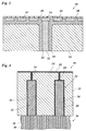
control unit 16 is mounted inside thedrum body 12, it has to be so adjusted that each of its conductors or terminals makes contact with the conductive material in only one of thelarge diameter holes 26. Because of the comparatively large diameter of these holes, the positional tolerance for the control unit is significantly larger than the pitch of theelectrodes 14. - As is shown in Figs. 3 and 4, the
electrodes 14 are formed as grooves separated by theridges 20 and filled with electricallyconductive material 28. Fig. 3 also shows thedielectric layer 30 covering theelectrodes 14 and theridges 20 as well as the electricallyconductive material 32 with which thesmall diameter portions 24 and thelarge diameter portions 26 of the through-holes 22 are filled. Theconductive material 28 forming theelectrodes 14 and filling the through-holes is electrically insulated from thealuminum drum body 12 by an anodised surface layer 34 (Al2O3) which is present at the outer circumferential surface of the drum body and at the internal walls of the through-holes. - As is shown in Fig. 4, a so-called zebra-
strip 36 is disposed at the inner wall surface of thedrum body 12 in order to provide an electrical connection between theconductive material 32 filled in thelarge diameter holes 26 and the conductors of thecontrol unit 16. This zebra-strip 36 is made of a resilient material which is elastically pressed between the internal wall of thedrum body 12 and theterminal array 18 of thecontrol unit 16 and is composed of alternatinglayers 38 which are made electrically conductive and insulatinglayers 40. Thus, if the terminals of the control unit are arranged to overlap with theholes 26, each conductor is safely connected with the corresponding one of theholes 26 and accordingly with theelectrode 14 associated therewith. In the shown embodiment, eachhole 26 overlaps with threeconductive layers 38 of the zebra-strip, so that an electrical connection is assured via three parallel electrical paths. In order to keep theadjacent electrodes 14 electrically separated from each other, it is of course necessary to provide separate zebra-strips 36 for each of the rows of through-holes 22 shown in Fig. 2. - The zebra-
strips 36 may be replaced by a material which has anisotropic electric conductivity such as an electrically anisotropic laquer. - A reliable and efficient method for manufacturing an image-forming element as described above will now be explained in conjunction with Fig. 3 and 4.
- At first, the hollow
cylindrical drum body 12 is formed as a one-piece member. Thegrooves 14 which are to form the electrodes are then cut into the circumferential surface of thedrum body 12 for example by means of a diamond chisel. Alternatively, these grooves may be formed by means of a laser beam or an electron beam. It should be noted, that, at this stage, thedrum body 12 has not yet been anodised so that thegrooves 14 are formed in a metal surface which can be machined more easily and more precisely than a metal oxide layer. - In the next step, the large diameter holes 26 are cut into the wall of the
drum body 12 from inside, for example by means of a laser beam. Theholes 26 are at first formed as blind bores, and the smaller emitter holes 24 are then formed in a second step. The small diameter holes 24 may also be formed with a laser beam, either form inside or outside of the drum. If they are cut from outside of the drum, the positional relationship between the small diameter holes 24 and thegrooves 14 can readily be confirmed. In this case, it will also be possible to form the small diameter holes 24 by punching or cutting with a diamond chisel or the like, instead of using a laser beam or an electron beam. - On the other hand, if the small diameter holes 24 are formed from inside of the drum, it is possible to form the large diameter holes 26 and the small diameter holes 24 in a single step, e.g. by means of a convergent laser beam, or two beams from different laser types aligned along the same optical axis.
- After the through-
holes 22 including thesmall diameter portions 24 and thelarge diameter portions 26 have been formed, thewhole drum body 12 is anodised according to known anodising techniques, so as to form the insulatingmetal oxide layer 32 on the whole surface of the drum body, especially on the outer circumferential surface forming thegrooves 14 and theridges 20 and on the internal walls of the through-holes 22. - In the next step, the electrically
conductive material grooves 14 and into the through-holes 22 so as to complete the electrodes and the electrical through-contacts. - Finally, the insulating
dielectric layer 30, which for example may be formed of AlN, Al2O3 or of SiOx as described in EP-A-0635768 is formed over theelectrodes 14 and theridges 20, and thecontrol unit 16 is mounted inside of the drum body to be connected to the through-contacts via the zebra-strips 36. - Depending on the diameter of the
drum body 12 and the dimensions of the tools used for forming the large diameter holes 26, it may be necessary that thedrum body 12 is composed of two or more segments in order to provide free access to the internal surface. In this case, the large diameter holes 26 are formed by means of a laser beam or electron beam in the individual segments, and then the segments are joined and welded together, preferably by electron beam welding, in order to form the hollowcylindrical drum body 12. In the example shown in Fig. 1, the drum body is composed of twosegments 12a joined together alongweld seams 12b. - The outer surface of the
drum body 12 is ground and finished in order to obtain an exact cylindrical shape, and then thegrooves 14 are cut. These steps are preferably performed on a lathe. - The subsequent steps of the manufacturing process may be the same as have been described above.
- Alternatively, the drum body may be anodised immediately after the
grooves 14 have been cut, i.e. before the small diameter holes 24 have been formed. In this case, the anodising process must be so controlled that the insulating oxide layer penetrates into the aluminum body at least to the level of the outer ends of the large diameter holes 26. The small diameter holes 24 are then formed in the oxide layer by laser cutting, punching or the like. Thus, when theconductive material 32 is filled in, it is assured that this material is perfectly insulated from thealuminum body 12. - A modified embodiment of an image-forming element and a processes for manufacturing the same will now be described in conjunction with Fig. 5 to 7.
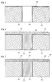
- The main difference to the manufacturing processes described above is that the
large diameter hole 26 is at first formed through the entire wall thickness of thedrum body 12, as is shown in Fig. 5. Thedrum body 12 is then anodised to form an insulatinglayer 42 on the outer circumferential surface of the drum body as well as the insulatingsurface layer 34 on the internal walls of theholes 26. Theholes 26 are filled with the electricallyconductive material 32, as is shown in Fig. 6. Then, alayer 44 of metallic aluminum is disposed on thelayer 42 on the outer surface of the drum body, for example by physical vapour deposition. Thereafter, thegrooves 14 are cut into thelayer 44, as is also shown in Fig. 6. - The
drum body 12 is then subjected to a second anodising step in which the whole thickness of thelayer 44 is transformed into an electrically insulating metal oxide. Finally, the small diameter holes 24 are formed through the insulatinglayer 44 and are filled with electrically conductive material to achieve the configuration shown in Fig. 7. - In this embodiment, the same techniques as in the previous embodiment may be used for forming the large diameter holes 26 and the small diameter holes 24. Thus, the
drum body 12 may either be an integral hollow cylindrical body from the outset or may be composed of several segments welded together after theholes 26 have been formed. - According to a modification of the manufacturing process, the large diameter holes 26 and the small diameter holes 24 may be formed in the same way as has been described in conjunction with Fig. 3 and 4, but without forming the
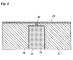
grooves 14 in the outer surface of the drum body. If the drum body is composed of several segments, these segments may be welded together either before or after the small diameter holes 24 have been formed. The drum body is then subjected to a first anodising step, and the large diameter holes 26 and the small diameter holes 24 are filled withconductive material 32. Then, as is shown in Fig. 8, acontinuous layer 46 of metallic aluminum is applied on the outer surface of thedrum body 12, thus covering the open ends of the small diameter holes 24. - Subsequently, the
grooves 14 are cut into thelayer 46, so that the outward ends of the small diameter holes 24 are again exposed at the bottoms of the grooves. The remaining parts of the layer 46 (i.e. the ridges 20) are then made electrically insulating in a second surface treatment step (e.g. an oxidising or anodising step), so that a configuration similar to that of Fig. 7 is achieved. - Finally, the
grooves 14 are filled withconductive material 28, and thedielectric layer 30 is applied as has been described in conjunction with Fig. 3. In a particular embodiment thegrooves 14, e.g. by physical vapour deposition, are filled with aluminium and the deposition of aluminum is continued until a thin layer (of about 0,8 to 3 µm thickness) is formed over the ridges. A dielectric layer is now formed by anodising the thus deposited aluminum to such a depth that the layer thickness covering the ridges is fully anodised. - While only specific embodiments of the invention have been described above, it will occur to a person skilled in the art that the described examples may be modified in various ways without departing from the scope of the invention as defined in the appended claims. For example, the
control unit 16 may be divided into several blocks angularly offset from one another and extending each over a different part of the length of the drum body. The through-holes 22 will then be arranged in accordance with this pattern.
Claims (8)
- Method for manufacturing a image-forming element (10) having a hollow cylindrical drum body (12) with a metallic outer layer and provided on its outer circumferential surface with a plurality of circumferentially extending electrodes which are electrically insulated from one another and from the drum body, comprising the steps of:- cutting grooves (14) into said metallic outer layer of the drum body (12),- forming an insulating surface layer (34) at least on the internal walls of said grooves (14) by converting the surface of said metallic outer layer into an insulating substance, and- filling said grooves with electrically conductive material (28).
- Method according to claim 1, wherein the insulating surface layer (34) is formed by anodising said metallic outer layer.
- Method according to claim 1, wherein through-holes (22) are formed in the wall of the drum body (12), the internal walls of these through-holes are anodised concurrently with the internal walls of the grooves (14), and the through-holes (22) are filled with electrically conductive material (32) for connecting each electrode to a control unit (16) disposed inside of the drum body (12).
- Method according to claim 1 or 2, wherein a metal layer (44; 46) is deposited on the outer surface of the drum body (12), and the grooves (14) are cut into the deposited layer (44; 46).
- Method according to any of the claims 1 to 3, wherein the grooves (14) are formed by laser beam cutting.
- Method according to any of the claims 1 to 3, wherein the grooves (14) are formed by electron beam cutting.
- Method according to any of the claims 1 to 3, wherein the grooves (14) are formed by mechanical cutting, preferably with a diamond chisel.
- Method according to any one of the preceding claims wherein the grooves (14) and the ridges between the grooves are filled and covered with metal and a dielectric surface layer is formed by anodising the metal to a depth equal to the layer thickness covering the ridges.
Priority Applications (1)
| Application Number | Priority Date | Filing Date | Title |
|---|---|---|---|
| EP97201202A EP0803782A1 (en) | 1996-04-25 | 1997-04-22 | Method for manufacturing an image-forming element |
Applications Claiming Priority (3)
| Application Number | Priority Date | Filing Date | Title |
|---|---|---|---|
| EP96201108 | 1996-04-25 | ||
| EP96201108 | 1996-04-25 | ||
| EP97201202A EP0803782A1 (en) | 1996-04-25 | 1997-04-22 | Method for manufacturing an image-forming element |
Publications (1)
| Publication Number | Publication Date |
|---|---|
| EP0803782A1 true EP0803782A1 (en) | 1997-10-29 |
Family
ID=26142737
Family Applications (1)
| Application Number | Title | Priority Date | Filing Date |
|---|---|---|---|
| EP97201202A Withdrawn EP0803782A1 (en) | 1996-04-25 | 1997-04-22 | Method for manufacturing an image-forming element |
Country Status (1)
| Country | Link |
|---|---|
| EP (1) | EP0803782A1 (en) |
Cited By (1)
| Publication number | Priority date | Publication date | Assignee | Title |
|---|---|---|---|---|
| WO2013156311A1 (en) | 2012-04-19 | 2013-10-24 | Oce-Technologies B.V. | An image forming device comprising a direct image forming element |
Citations (3)
| Publication number | Priority date | Publication date | Assignee | Title |
|---|---|---|---|---|
| EP0247699A1 (en) * | 1986-05-29 | 1987-12-02 | Océ-Nederland B.V. | Image-forming element for an electrostatic printer, and a printer in which an element of this kind is used |
| EP0595388A1 (en) * | 1992-10-30 | 1994-05-04 | Océ-Nederland B.V. | A process for the preparation of an image-forming element and a printing device for reproducing information |
| EP0635768A1 (en) * | 1993-07-23 | 1995-01-25 | Océ-Nederland B.V. | Image-forming device and an image-recording element for use therein |
-
1997
- 1997-04-22 EP EP97201202A patent/EP0803782A1/en not_active Withdrawn
Patent Citations (3)
| Publication number | Priority date | Publication date | Assignee | Title |
|---|---|---|---|---|
| EP0247699A1 (en) * | 1986-05-29 | 1987-12-02 | Océ-Nederland B.V. | Image-forming element for an electrostatic printer, and a printer in which an element of this kind is used |
| EP0595388A1 (en) * | 1992-10-30 | 1994-05-04 | Océ-Nederland B.V. | A process for the preparation of an image-forming element and a printing device for reproducing information |
| EP0635768A1 (en) * | 1993-07-23 | 1995-01-25 | Océ-Nederland B.V. | Image-forming device and an image-recording element for use therein |
Cited By (2)
| Publication number | Priority date | Publication date | Assignee | Title |
|---|---|---|---|---|
| WO2013156311A1 (en) | 2012-04-19 | 2013-10-24 | Oce-Technologies B.V. | An image forming device comprising a direct image forming element |
| US9280083B2 (en) | 2012-04-19 | 2016-03-08 | Oce-Technologies B.V. | Image forming device comprising a direct image forming element |
Similar Documents
| Publication | Publication Date | Title |
|---|---|---|
| US6014157A (en) | Image forming element having accurate connection with the electronic components of the control unit | |
| EP0803783B1 (en) | Image-forming element and method for manufacturing the same | |
| JP2719615B2 (en) | Image forming element manufacturing method and information reproducing printing apparatus | |
| KR20010021548A (en) | Ptc thermistor chip and method for manufacturing the same | |
| KR20050022324A (en) | A process for manufacturing a wiring board having a via | |
| US6045679A (en) | Method for manufacturing an image-forming element | |
| EP0803782A1 (en) | Method for manufacturing an image-forming element | |
| US7828707B2 (en) | Image drum for selectively absorbing toner thereon | |
| US6867133B2 (en) | Method of manufacturing chip inductor | |
| US20090220683A1 (en) | Method of manufacturing electronic part and electronic part | |
| CN110192313B (en) | Method for manufacturing spark plug | |
| JP3633989B2 (en) | Electrical discharge machining method for insulating ceramics | |
| JP3046957B2 (en) | Charge plate of jet liquid charging device and method of manufacturing the same | |
| JP3583279B2 (en) | Drilling method | |
| JPH1022610A (en) | Manufacture of printed circuit board | |
| JPS61235163A (en) | Manufacture of high-density wiring block | |
| JPH07136849A (en) | Electric discharge machining and device therefor | |
| US20060128143A1 (en) | Production method for electronic component and electronic component | |
| EP0184589A2 (en) | Electroerosion printhead with tungsten electrodes and a method for making the same | |
| JPS5918226B2 (en) | Recording head manufacturing method | |
| EP0292597A1 (en) | Magnetic print head comprising at least one linear array of magnetic printing elements | |
| JPS61224490A (en) | Manufacture of head for ion flow recording | |
| JPH0667642B2 (en) | Ion flow recording head manufacturing method | |
| KR20020039621A (en) | Technique for manufacturing an electrostatic element for steering a charged particle beam | |
| JPS63221053A (en) | Manufacture of electrode head |
Legal Events
| Date | Code | Title | Description |
|---|---|---|---|
| PUAI | Public reference made under article 153(3) epc to a published international application that has entered the european phase |
Free format text: ORIGINAL CODE: 0009012 |
|
| AK | Designated contracting states |
Kind code of ref document: A1 Designated state(s): DE FR GB IT NL SE |
|
| 17P | Request for examination filed |
Effective date: 19980418 |
|
| 17Q | First examination report despatched |
Effective date: 20011002 |
|
| STAA | Information on the status of an ep patent application or granted ep patent |
Free format text: STATUS: THE APPLICATION IS DEEMED TO BE WITHDRAWN |
|
| 18D | Application deemed to be withdrawn |
Effective date: 20091204 |