EP0635768A1 - Image-forming device and an image-recording element for use therein - Google Patents
Image-forming device and an image-recording element for use therein Download PDFInfo
- Publication number
- EP0635768A1 EP0635768A1 EP94201851A EP94201851A EP0635768A1 EP 0635768 A1 EP0635768 A1 EP 0635768A1 EP 94201851 A EP94201851 A EP 94201851A EP 94201851 A EP94201851 A EP 94201851A EP 0635768 A1 EP0635768 A1 EP 0635768A1
- Authority
- EP
- European Patent Office
- Prior art keywords
- image
- layer
- forming
- dielectric surface
- recording element
- Prior art date
- Legal status (The legal status is an assumption and is not a legal conclusion. Google has not performed a legal analysis and makes no representation as to the accuracy of the status listed.)
- Granted
Links
- 239000010410 layer Substances 0.000 claims abstract description 61
- 239000002344 surface layer Substances 0.000 claims abstract description 25
- VYPSYNLAJGMNEJ-UHFFFAOYSA-N Silicium dioxide Chemical compound O=[Si]=O VYPSYNLAJGMNEJ-UHFFFAOYSA-N 0.000 claims abstract description 20
- 229910052814 silicon oxide Inorganic materials 0.000 claims abstract description 18
- 239000000463 material Substances 0.000 claims abstract description 14
- 239000000843 powder Substances 0.000 claims description 12
- 150000004767 nitrides Chemical class 0.000 claims description 3
- QVGXLLKOCUKJST-UHFFFAOYSA-N atomic oxygen Chemical compound [O] QVGXLLKOCUKJST-UHFFFAOYSA-N 0.000 description 7
- 229910052751 metal Inorganic materials 0.000 description 7
- 239000002184 metal Substances 0.000 description 7
- 238000000034 method Methods 0.000 description 7
- 239000001301 oxygen Substances 0.000 description 7
- 229910052760 oxygen Inorganic materials 0.000 description 7
- 239000003822 epoxy resin Substances 0.000 description 6
- 229920000647 polyepoxide Polymers 0.000 description 6
- RYGMFSIKBFXOCR-UHFFFAOYSA-N Copper Chemical compound [Cu] RYGMFSIKBFXOCR-UHFFFAOYSA-N 0.000 description 5
- XUIMIQQOPSSXEZ-UHFFFAOYSA-N Silicon Chemical compound [Si] XUIMIQQOPSSXEZ-UHFFFAOYSA-N 0.000 description 4
- 230000000694 effects Effects 0.000 description 4
- 230000005291 magnetic effect Effects 0.000 description 4
- 229910052710 silicon Inorganic materials 0.000 description 4
- 239000010703 silicon Substances 0.000 description 4
- PNEYBMLMFCGWSK-UHFFFAOYSA-N Alumina Chemical compound [O-2].[O-2].[O-2].[Al+3].[Al+3] PNEYBMLMFCGWSK-UHFFFAOYSA-N 0.000 description 3
- OKTJSMMVPCPJKN-UHFFFAOYSA-N Carbon Chemical compound [C] OKTJSMMVPCPJKN-UHFFFAOYSA-N 0.000 description 3
- 229910052799 carbon Inorganic materials 0.000 description 3
- 229910052802 copper Inorganic materials 0.000 description 3
- 239000010949 copper Substances 0.000 description 3
- 238000002149 energy-dispersive X-ray emission spectroscopy Methods 0.000 description 3
- 239000003292 glue Substances 0.000 description 3
- 238000004544 sputter deposition Methods 0.000 description 3
- XKRFYHLGVUSROY-UHFFFAOYSA-N Argon Chemical compound [Ar] XKRFYHLGVUSROY-UHFFFAOYSA-N 0.000 description 2
- IJGRMHOSHXDMSA-UHFFFAOYSA-N Atomic nitrogen Chemical compound N#N IJGRMHOSHXDMSA-UHFFFAOYSA-N 0.000 description 2
- XLOMVQKBTHCTTD-UHFFFAOYSA-N Zinc monoxide Chemical compound [Zn]=O XLOMVQKBTHCTTD-UHFFFAOYSA-N 0.000 description 2
- 230000002411 adverse Effects 0.000 description 2
- 229910052782 aluminium Inorganic materials 0.000 description 2
- XAGFODPZIPBFFR-UHFFFAOYSA-N aluminium Chemical compound [Al] XAGFODPZIPBFFR-UHFFFAOYSA-N 0.000 description 2
- 238000005234 chemical deposition Methods 0.000 description 2
- 239000004020 conductor Substances 0.000 description 2
- 239000011889 copper foil Substances 0.000 description 2
- 238000005530 etching Methods 0.000 description 2
- 238000007667 floating Methods 0.000 description 2
- 238000010438 heat treatment Methods 0.000 description 2
- 239000007788 liquid Substances 0.000 description 2
- 239000000203 mixture Substances 0.000 description 2
- 230000003287 optical effect Effects 0.000 description 2
- 239000002245 particle Substances 0.000 description 2
- 239000000758 substrate Substances 0.000 description 2
- 238000007514 turning Methods 0.000 description 2
- 229910052581 Si3N4 Inorganic materials 0.000 description 1
- BQCADISMDOOEFD-UHFFFAOYSA-N Silver Chemical compound [Ag] BQCADISMDOOEFD-UHFFFAOYSA-N 0.000 description 1
- 239000004411 aluminium Substances 0.000 description 1
- 229910052786 argon Inorganic materials 0.000 description 1
- 239000011230 binding agent Substances 0.000 description 1
- 239000006229 carbon black Substances 0.000 description 1
- 239000011248 coating agent Substances 0.000 description 1
- 238000000576 coating method Methods 0.000 description 1
- 229910052681 coesite Inorganic materials 0.000 description 1
- 229920001940 conductive polymer Polymers 0.000 description 1
- 238000010276 construction Methods 0.000 description 1
- 229910052906 cristobalite Inorganic materials 0.000 description 1
- 238000000151 deposition Methods 0.000 description 1
- 230000008021 deposition Effects 0.000 description 1
- 238000005137 deposition process Methods 0.000 description 1
- 238000005516 engineering process Methods 0.000 description 1
- 238000002474 experimental method Methods 0.000 description 1
- 230000005294 ferromagnetic effect Effects 0.000 description 1
- 238000003754 machining Methods 0.000 description 1
- 238000004519 manufacturing process Methods 0.000 description 1
- 239000002923 metal particle Substances 0.000 description 1
- 229910052757 nitrogen Inorganic materials 0.000 description 1
- 230000002093 peripheral effect Effects 0.000 description 1
- 238000001259 photo etching Methods 0.000 description 1
- -1 potassium ferricyanide Chemical compound 0.000 description 1
- 150000003856 quaternary ammonium compounds Chemical class 0.000 description 1
- 239000000377 silicon dioxide Substances 0.000 description 1
- 235000012239 silicon dioxide Nutrition 0.000 description 1
- HQVNEWCFYHHQES-UHFFFAOYSA-N silicon nitride Chemical compound N12[Si]34N5[Si]62N3[Si]51N64 HQVNEWCFYHHQES-UHFFFAOYSA-N 0.000 description 1
- 229910052709 silver Inorganic materials 0.000 description 1
- 239000004332 silver Substances 0.000 description 1
- 229910052682 stishovite Inorganic materials 0.000 description 1
- 229910052905 tridymite Inorganic materials 0.000 description 1
- 239000011787 zinc oxide Substances 0.000 description 1
Images

Classifications
-
- G—PHYSICS
- G03—PHOTOGRAPHY; CINEMATOGRAPHY; ANALOGOUS TECHNIQUES USING WAVES OTHER THAN OPTICAL WAVES; ELECTROGRAPHY; HOLOGRAPHY
- G03G—ELECTROGRAPHY; ELECTROPHOTOGRAPHY; MAGNETOGRAPHY
- G03G15/00—Apparatus for electrographic processes using a charge pattern
- G03G15/22—Apparatus for electrographic processes using a charge pattern involving the combination of more than one step according to groups G03G13/02 - G03G13/20
- G03G15/34—Apparatus for electrographic processes using a charge pattern involving the combination of more than one step according to groups G03G13/02 - G03G13/20 in which the powder image is formed directly on the recording material, e.g. by using a liquid toner
- G03G15/344—Apparatus for electrographic processes using a charge pattern involving the combination of more than one step according to groups G03G13/02 - G03G13/20 in which the powder image is formed directly on the recording material, e.g. by using a liquid toner by selectively transferring the powder to the recording medium, e.g. by using a LED array
- G03G15/348—Apparatus for electrographic processes using a charge pattern involving the combination of more than one step according to groups G03G13/02 - G03G13/20 in which the powder image is formed directly on the recording material, e.g. by using a liquid toner by selectively transferring the powder to the recording medium, e.g. by using a LED array using a stylus or a multi-styli array
-
- G—PHYSICS
- G03—PHOTOGRAPHY; CINEMATOGRAPHY; ANALOGOUS TECHNIQUES USING WAVES OTHER THAN OPTICAL WAVES; ELECTROGRAPHY; HOLOGRAPHY
- G03G—ELECTROGRAPHY; ELECTROPHOTOGRAPHY; MAGNETOGRAPHY
- G03G2217/00—Details of electrographic processes using patterns other than charge patterns
- G03G2217/0075—Process using an image-carrying member having an electrode array on its surface
Definitions
- the invention relates to an image-forming device having a movable image-recording element comprising a support with a dielectric surface layer beneath which there is disposed a system of separately energisable image-forming electrodes, an image-forming zone situated along the path of movement of the image-recording element, in which zone a counter electrode is disposed a short distance above the dielectric surface of the image-recording element, energisation means for applying a voltage between the image-forming electrodes and the counter electrode in accordance with an image pattern to be recorded, in order that toner powder supplied in the image-forming zone may be deposited on the surface of the image-recording element in accordance with the image pattern.
- the invention also relates to an image-recording element for use in such an image-forming device.
- Image-forming devices and image-recording elements usable therein as referred to above are described, inter alia, in European patents 0 191 521, 0 247 694 and 0 247 699.
- a toner powder image recorded on the image-recording element in the image-forming zone is transferred directly or indirectly via an intermediate to a receiving material, such as ordinary paper, and fixed thereon.
- the image-recording element is then used again for a subsequent image-recording cycle.
- this type of image-forming devices of course, the longest possible life is required for the image-recording element.
- a floating image-forming electrode provides no further contribution to the image-forming, and this becomes visible on the print in the form of a fine tonerfree streak in the image pattern.
- toner is deposited in the imagefree portions, so that a fine toner streak is formed on the print in those portions.
- One floating image-forming electrode therefore, already makes it desirable to replace the image-recording element.
- the invention provides an improved image-forming device of the kind referred to in the preamble, having an improved image-recording element so that the above adverse effects visible on the print due to the fact that an image-forming electrode cannot be directly energised no longer occur or at least hardly to a disturbing degree.
- the device according to the invention is characterised in that the separately energisable image-forming electrodes beneath the dielectric surface layer are interconnected in the image-recording element by a material whose electrical resistance is between that of the dielectric surface layer and that of the image-forming electrode and this resistance is so selected that an image-forming electrode that cannot be directly energised by the energisation means is energised at such a level, on energisation of the nearest image-forming electrode, that toner powder is deposited on the dielectric surface situated thereabove.
- the image-forming electrodes are interconnected by a material situated directly beneath the dielectric surface layer and having a resistance between that of the dielectric surface layer and that of the image-forming electrodes. The resistance is so selected that an image-forming electrode which can no longer be directly controlled by the energising means is energised to such a level, on energisation of the nearest image-forming electrode, that toner powder is deposited on the dielectric surface thereabove.
- the resistance to be selected depends on the distance between the image-forming electrodes, the resistance of both the image-forming electrodes and the dielectric surface layer, and the electrical conductivity of the toner powder used for the image-recording. It has been found that with image-forming elements as described in the above prior art, in which the dielectric surface layer has a resistivity between 109 and 1012 ⁇ .cm and a thickness between 0.2 and 0.8 ⁇ m, the distance between successive image-forming electrodes is 15-25 ⁇ m and the toner powder used for the image-recording has a resistivity of between 103 and 106 ⁇ .cm (measured as described in European patent application 0 441 426), this resistance should be a factor of 102 to 104 lower than that of the dielectric surface layer.
- the lower resistance material connecting the image-forming electrodes can be disposed directly beneath the dielectric surface layer between the image-forming electrodes, but according to one preferred embodiment of the invention, the material is applied as a continuous layer over an insulating substrate in which the image-forming electrodes are embedded at the surface. In the latter case, the thickness of the applied layer is preferably 0.2 to 0.5 ⁇ m.
- the disadvantage of a thicker layer is that the distance between an image-forming electrode and the surface of the dielectric layer still to be applied becomes relatively large, and this may have an adverse effect on the sharpness of the images to be recorded.
- the lower resistance material can, in principle, consist of any material having the required electrical resistance.
- the dielectric surface layer and the layer of connecting material therebeneath are in the form of a continuous layer having an increasing resistance towards the surface.
- a layer of this kind can be formed by a known chemical deposition process, such as sputtering or vapour coating, the conditions of the deposition process being so controlled that the resulting layer has in the bottom portion of the layer a resistance lower by the required level (e.g. a factor of 102-104) than in the top part of the layer.
- a thin layer is formed, for example, by a known sputtering process, consisting of an oxide or nitride, such as silicon oxide, aluminium oxide, silicon nitride and zinc oxide, the oxygen or nitrogen proportion of which in the molecular lattice increases from bottom to top, or is relatively low in the bottom half and relatively high in the top half, thus giving the required differential resistance.
- the thin layer applied by a chemical deposition process consists of a layer of silicon oxide about 0.8 ⁇ m thick the bottom portion of the layer in a thickness of 0.2-0.5 ⁇ m consisting of SiO x , where x is approximately 0.40-0.65, and the top part of the layer consisting of SiO x , where x is approximately 1.2-1.6.
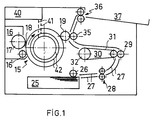
- the image-forming device is provided with the image-recording element 15, which will be described hereinafter in detail with reference to Fig. 2.
- the image-recording element 15 passes through an image-forming station 16, where its surface is provided with a uniform layer of toner powder having a resistivity of about 105 ⁇ .cm, by means 16' constructed as described in US patent 3 946 402.
- the powdered surface of the image-recording element 15 is then fed to an image-forming zone 18, where a magnetic roller 17 is disposed at a short distance from the surface of the image-recording element 15, said roller 17 comprising a rotatable electrically conductive non magnetic sleeve and a stationary magnet system disposed inside the sleeve.
- the stationary magnet system comprises a ferromagnetic knife blade clamped between like poles of two magnets and is constructed as described in European patent application 0 304 983.
- a voltage between one or more image-forming electrodes of the image-recording element 15 and the conductive sleeve of the magnetic roller 17 acting as a counter electrode By application of a voltage between one or more image-forming electrodes of the image-recording element 15 and the conductive sleeve of the magnetic roller 17 acting as a counter electrode, a powder image is formed on the image-recording element.
- the magnetic roller 17 and the image-forming electrodes of the image-recording element 15 are at earth potential.
- the image-forming electrodes involved are brought to a positive potential of about 30 volts. This powder image is transferred, by the application of pressure,to a heated rubber covered roller 19.
- a sheet of paper is taken from a supply stack 25 by roller 26 and fed to a heating station 30 via guideways 27 and rollers 28,29.
- Heating station 30 comprises a belt 31 running about a heated roller 32.
- the sheet of paper is heated by contact with the belt 31.
- the sheet heated in this way is then fed through the roller 19 and a pressure roller 35, the softened powder image on the roller 19 being completely transferred to the sheet of paper.
- the temperatures of the belt 31 and the roller 19 are so adapted to one another that the image fuses to the sheet of paper.
- the sheet of paper provided with an image is fed to a collecting tray 37 via conveyor rollers 36.
- Unit 40 comprises an electronic circuit which converts the optical information of an original into electrical signals which are fed to the control elements 3 (see Fig.
- the image-recording element used in the image-forming device according to Fig. 1 is shown in diagrammatic cross-section in Fig. 2.
- the image-recording element 1 shown in Fig. 2 comprises a cylinder 2 having, mounted therein, a control element 3 which extends axially and which has a construction which will be described in detail hereinafter.
- the cylinder 2 is covered with an insulating layer 4, on which image-forming electrodes 5 are disposed and extend in the form of endless tracks parallel to one another at substantially equal spacing in the peripheral direction of the cylinder 2.
- One image-forming electrode 5 in each case is conductively connected to one control electrode 6 of the control element 3.
- the number of control electrodes 6 of the control element 3 is equal to the number of image-forming electrodes 5, such number governing the quality of the images to be formed on the image-recording element 1. Image quality improves with increasing electrode density. To achieve a good quality, the number of image-forming electrodes 5 is at least 10 per mm and preferably 14 to 20 per mm. According to one specific embodiment the number of electrodes 5 is equal to 16 per mm, the electrodes 5 having a width of 40 ⁇ m and the distance between the electrodes being about 20 ⁇ m. Finally, the pattern of image-forming electrodes 5 is covered with a top layer 7.
- the control element 3 comprises a support 10 which is provided in known manner with an electrically conductive metal layer (such as copper), which metal layer is then converted to the required conductive track pattern 12 in the manner to be described hereinafter.
- the track pattern 12 consists, on the one hand, of the conductive connections between the various electronic components 13 of the control element 3 and, on the other hand, the control electrodes 6, one of which in each case being conductively connected to one image-forming electrode 5.
- the control element 3 also comprises a cover 14 which is connected to the support 10 in known manner (e.g. glued), to form a box-shaped control element 3 in which the electronic components are enclosed.
- the electronic components 13 comprise a number of integrated circuits known, for example, from video display technology, comprising a serial-in parallel-out shift register, an output register, and, connected thereto, drivers having a voltage range of 25 to 50 volts for example.
- One control electrode 6 is connected to one driver of one of the integrated circuits.
- the image-recording element 1 is made as follows.
- a control element 3 is made from a metal core substrate consisting of an aluminum support plate on which a copper foil is glued by means of an epoxy resin specially developed for the electronics industry, known as an "electronic grade" epoxy resin, said control element 3 being made by converting the copper foil, by a known photoetching technique, into a conductive track pattern 12 which comprises both the conductive connecting tracks for the electronic components 13 to be placed on the support 10, and the conductive tracks for the control electrodes 6.
- the electronic components 13 are then fixed on the support 10 at the correct place determined by the conductive connecting tracks, and the cover 14 is glued to the support 10 with an electronic grade epoxy resin.
- the control element 3 in box form thus made is then placed in an axial slot formed in the wall of the aluminium cylinder 2, and is glued therein by means of the abovementioned epoxy resin glue.
- the axial slot is at least as long as the operative width of the image-recording element 1.
- the space between the control element 3 and the wall of the slot must be so dimensioned that the said space can be filled by the glue by capillary action. Too large a space results in the glue running out.
- the outer surface of the cylinder 2 with the control element 3 fixed therein is then turned to a predetermined degree and brought into contact with a suitable etching liquid, (e.g.
- etching liquid is so selected that the metal of the control electrodes 6 is only slightly affected, so that the ends of these electrodes are finally projecting about 150 ⁇ m above the surface of the cylinder 2 and the control element 3.
- the surface of the cylinder 2 is then covered with an insulating intermediate layer 4 of electronic grade epoxy resin having a layer thickness corresponding to the length of the projecting ends of the electrodes 6, so that the end faces thereof lie at the outer surface of the insulating intermediate layer 4.
- the image-forming electrodes 5 are formed by machining (e.g. on a lathe) a number of peripherally and parallel extending endless grooves in the outer surface of the intermediate layer 4.
- the groove pattern is so applied that it corresponds completely (as regards density and location) to the pattern of control electrodes 6, so that one control electrode 6 cooperates with one groove.
- the grooves are filled by copper vapour deposition and removal of the surface by turning, thus producing the conductive image-forming electrodes 5.
- the pattern of image-forming electrodes is finally covered with a smooth top layer 7.
- the silicon oxidelayer is applied by a known sputter technique in a vacuum chamber, e.g.
- the quantity of oxygen to be introduced to achieve the required SiO x composition can be determined by experiment by making a number of samples by varying the quantity of oxygen introduced and determining the silicon/oxygen ratio of the SiO x layer on the various samples by EDX analysis (Energy Dispersive X-ray Analysis).
- the analyser (Tracor TN 5500 of Tracor Europe, Amersfoort, Netherlands) is calibrated with a reference standard of at least 99.9% SiO2.
- a layer of carbon some tens of nanometres thick is vapour coated over the SiO x layer of the samples to be measured, as is known with EDX analysis. This vapour coated carbon layer is also present on the reference standard.
- a first image-recording element was made as described above, and during the production of the control element 3, the connection between some of the control electrodes 6 distributed over the element and the control electronics 30 was broken by removing part of the metal track.
- FIG. 3 shows another possible embodiment of a suitable image-recording element.
- This image-recording element differs from the element described with reference to Fig. 2 solely in that a thin layer of connecting material is applied between the image-forming electrodes and directly beneath the dielectric surface layer. Up to and including the application of the insulating layer 4 this image-recording element was made in the same way as the element shown in Fig. 2.
- a layer 8 about 1 ⁇ m thick of epoxy resin with carbon particles dispersed therein was then applied over the insulating layer 4, and had a resistance of about 106 ⁇ .
- the grooves were then formed in the surface, the layer 8 being completely removed at the location of the grooves.
Landscapes
- Physics & Mathematics (AREA)
- General Physics & Mathematics (AREA)
- Printers Or Recording Devices Using Electromagnetic And Radiation Means (AREA)
- Electrophotography Using Other Than Carlson'S Method (AREA)
Abstract
Description
- The invention relates to an image-forming device having a movable image-recording element comprising a support with a dielectric surface layer beneath which there is disposed a system of separately energisable image-forming electrodes, an image-forming zone situated along the path of movement of the image-recording element, in which zone a counter electrode is disposed a short distance above the dielectric surface of the image-recording element, energisation means for applying a voltage between the image-forming electrodes and the counter electrode in accordance with an image pattern to be recorded, in order that toner powder supplied in the image-forming zone may be deposited on the surface of the image-recording element in accordance with the image pattern.
The invention also relates to an image-recording element for use in such an image-forming device.
Image-forming devices and image-recording elements usable therein as referred to above are described, inter alia, in European patents 0 191 521, 0 247 694 and 0 247 699. In these known devices, a toner powder image recorded on the image-recording element in the image-forming zone is transferred directly or indirectly via an intermediate to a receiving material, such as ordinary paper, and fixed thereon. The image-recording element is then used again for a subsequent image-recording cycle. With this type of image-forming devices, of course, the longest possible life is required for the image-recording element. One problem which arises is that the repeated mechanical, electrical and thermal loading to which the image-recording element is subjected causes one or more fractures to occur in the image-forming electrode or electrodes themselves or in the connection between the image-forming electrode or electrodes and the electric energising means, so that the electrode "floats" and is no longer energised. A floating image-forming electrode provides no further contribution to the image-forming, and this becomes visible on the print in the form of a fine tonerfree streak in the image pattern. In addition, it is regularly observed that toner is deposited in the imagefree portions, so that a fine toner streak is formed on the print in those portions. One floating image-forming electrode, therefore, already makes it desirable to replace the image-recording element. - The invention provides an improved image-forming device of the kind referred to in the preamble, having an improved image-recording element so that the above adverse effects visible on the print due to the fact that an image-forming electrode cannot be directly energised no longer occur or at least hardly to a disturbing degree.
- The device according to the invention is characterised in that the separately energisable image-forming electrodes beneath the dielectric surface layer are interconnected in the image-recording element by a material whose electrical resistance is between that of the dielectric surface layer and that of the image-forming electrode and this resistance is so selected that an image-forming electrode that cannot be directly energised by the energisation means is energised at such a level, on energisation of the nearest image-forming electrode, that toner powder is deposited on the dielectric surface situated thereabove.
- Disposing directly beneath the dielectric surface layer a material which is relatively conductive in relation to said layer and which interconnects the image-forming electrodes, has the effect that an image-forming electrode which can no longer be directly energised due to a break in the connection to the energising means is energised on energisation of the nearest electrode. Consequently, a quantity of toner is also deposited above the non operating image-forming electrode, so that the occurrence of disturbing toner-free streaks in image patterns is obviated. Another effect is that no toner is deposited in the image-free portions above an image-forming electrode which cannot be directly energised.
Thus, according to the invention, if an image-forming electrode can no longer be directly controlled, the consequences thereof on the print are not visible or are not visible to a disturbing degree, so that there is no need to replace the image-forming element immediately and hence a longer life is achieved. In the image-forming element of the image-forming device according to the invention, the image-forming electrodes are interconnected by a material situated directly beneath the dielectric surface layer and having a resistance between that of the dielectric surface layer and that of the image-forming electrodes. The resistance is so selected that an image-forming electrode which can no longer be directly controlled by the energising means is energised to such a level, on energisation of the nearest image-forming electrode, that toner powder is deposited on the dielectric surface thereabove. The resistance to be selected depends on the distance between the image-forming electrodes, the resistance of both the image-forming electrodes and the dielectric surface layer, and the electrical conductivity of the toner powder used for the image-recording. It has been found that with image-forming elements as described in the above prior art, in which the dielectric surface layer has a resistivity between 10⁹ and 10¹² Ω.cm and a thickness between 0.2 and 0.8 µm, the distance between successive image-forming electrodes is 15-25 µm and the toner powder used for the image-recording has a resistivity of between 10³ and 10⁶ Ω.cm (measured as described in European patent application 0 441 426), this resistance should be a factor of 10² to 10⁴ lower than that of the dielectric surface layer. The lower resistance material connecting the image-forming electrodes can be disposed directly beneath the dielectric surface layer between the image-forming electrodes, but according to one preferred embodiment of the invention, the material is applied as a continuous layer over an insulating substrate in which the image-forming electrodes are embedded at the surface. In the latter case, the thickness of the applied layer is preferably 0.2 to 0.5 µm. The disadvantage of a thicker layer is that the distance between an image-forming electrode and the surface of the dielectric layer still to be applied becomes relatively large, and this may have an adverse effect on the sharpness of the images to be recorded.
The lower resistance material can, in principle, consist of any material having the required electrical resistance. It may, for example, be formed from a binder in which conductive material is finely distributed, such as carbon black metal particles (e.g. copper or silver particles), metal complexes (e.g. as described in USpatent 3 245 833), quaternary ammonium compounds or conductive polymers or mixtures of such materials or other conductive materials known per se.
According to another preferred embodiment of the invention, the dielectric surface layer and the layer of connecting material therebeneath are in the form of a continuous layer having an increasing resistance towards the surface. A layer of this kind can be formed by a known chemical deposition process, such as sputtering or vapour coating, the conditions of the deposition process being so controlled that the resulting layer has in the bottom portion of the layer a resistance lower by the required level (e.g. a factor of 10²-10⁴) than in the top part of the layer. According to this preferred embodiment of the invention, a thin layer is formed, for example, by a known sputtering process, consisting of an oxide or nitride, such as silicon oxide, aluminium oxide, silicon nitride and zinc oxide, the oxygen or nitrogen proportion of which in the molecular lattice increases from bottom to top, or is relatively low in the bottom half and relatively high in the top half, thus giving the required differential resistance.
According to a very attractive embodiment of the invention, the thin layer applied by a chemical deposition process consists of a layer of silicon oxide about 0.8 µm thick the bottom portion of the layer in a thickness of 0.2-0.5 µm consisting of SiOx, where x is approximately 0.40-0.65, and the top part of the layer consisting of SiOx, where x is approximately 1.2-1.6.
The invention will be explained in detail with reference to the accompanying drawings wherein: - Fig. 1 is a diagrammatic illustration of the principle of an image-forming device according to the invention,
- Fig. 2 is a cross-section of a preferred embodiment of an image-recording element for use in the device according to Fig. 1, and
- Fig. 3 is a longitudinal cross-section of another embodiment of an image-recording element for use in the device according to Fig. 1.
- The image-forming device according to Fig. 1 is provided with the image-
recording element 15, which will be described hereinafter in detail with reference to Fig. 2. The image-recording element 15 passes through an image-formingstation 16, where its surface is provided with a uniform layer of toner powder having a resistivity of about 10⁵ Ω.cm, by means 16' constructed as described in USpatent 3 946 402.
The powdered surface of the image-recording element 15 is then fed to an image-formingzone 18, where amagnetic roller 17 is disposed at a short distance from the surface of the image-recording element 15, saidroller 17 comprising a rotatable electrically conductive non magnetic sleeve and a stationary magnet system disposed inside the sleeve. The stationary magnet system comprises a ferromagnetic knife blade clamped between like poles of two magnets and is constructed as described in European patent application 0 304 983. By application of a voltage between one or more image-forming electrodes of the image-recording element 15 and the conductive sleeve of themagnetic roller 17 acting as a counter electrode, a powder image is formed on the image-recording element. When no image is recorded, themagnetic roller 17 and the image-forming electrodes of the image-recording element 15 are at earth potential. During image-recording, the image-forming electrodes involved are brought to a positive potential of about 30 volts. This powder image is transferred, by the application of pressure,to a heated rubber coveredroller 19. A sheet of paper is taken from asupply stack 25 byroller 26 and fed to aheating station 30 viaguideways 27 androllers Heating station 30 comprises abelt 31 running about a heatedroller 32. The sheet of paper is heated by contact with thebelt 31. The sheet heated in this way is then fed through theroller 19 and apressure roller 35, the softened powder image on theroller 19 being completely transferred to the sheet of paper.
The temperatures of thebelt 31 and theroller 19 are so adapted to one another that the image fuses to the sheet of paper. The sheet of paper provided with an image is fed to a collectingtray 37 viaconveyor rollers 36.
Unit 40 comprises an electronic circuit which converts the optical information of an original into electrical signals which are fed to the control elements 3 (see Fig. 2), viawires 41 having sliding contacts, andconductive tracks 42 disposed in the side wall of the image-recording element 15, saidcontrol elements 3 being connected to thesaid tracks 42. The information is fed serially line by line to the shift register of the integrated circuits of theelements 3. If the shift registers are completely filled in accordance with the information of one line, that information is placed in the output register and voltage is either applied or not applied to theelectrodes 6,5 (see Fig. 2) via the drivers depending on the signal. While this line is being printed the information of the next line is fed to the shift registers.
Apart from optical information from an original, electrical signals originating from a computer or a dataprocessing device can also be converted inunit 40 to signals fed to thecontrol elements 3. - The image-recording element used in the image-forming device according to Fig. 1 is shown in diagrammatic cross-section in Fig. 2. The image-
recording element 1 shown in Fig. 2 comprises acylinder 2 having, mounted therein, acontrol element 3 which extends axially and which has a construction which will be described in detail hereinafter. Thecylinder 2 is covered with an insulating layer 4, on which image-formingelectrodes 5 are disposed and extend in the form of endless tracks parallel to one another at substantially equal spacing in the peripheral direction of thecylinder 2. One image-formingelectrode 5 in each case is conductively connected to onecontrol electrode 6 of thecontrol element 3. The number ofcontrol electrodes 6 of thecontrol element 3 is equal to the number of image-formingelectrodes 5, such number governing the quality of the images to be formed on the image-recording element 1. Image quality improves with increasing electrode density. To achieve a good quality, the number of image-formingelectrodes 5 is at least 10 per mm and preferably 14 to 20 per mm. According to one specific embodiment the number ofelectrodes 5 is equal to 16 per mm, theelectrodes 5 having a width of 40 µm and the distance between the electrodes being about 20 µm.
Finally, the pattern of image-formingelectrodes 5 is covered with a top layer 7. Thecontrol element 3 comprises asupport 10 which is provided in known manner with an electrically conductive metal layer (such as copper), which metal layer is then converted to the requiredconductive track pattern 12 in the manner to be described hereinafter. Thetrack pattern 12 consists, on the one hand, of the conductive connections between the variouselectronic components 13 of thecontrol element 3 and, on the other hand, thecontrol electrodes 6, one of which in each case being conductively connected to one image-formingelectrode 5.
Finally, thecontrol element 3 also comprises acover 14 which is connected to thesupport 10 in known manner (e.g. glued), to form a box-shaped control element 3 in which the electronic components are enclosed.
Theelectronic components 13 comprise a number of integrated circuits known, for example, from video display technology, comprising a serial-in parallel-out shift register, an output register, and, connected thereto, drivers having a voltage range of 25 to 50 volts for example. Onecontrol electrode 6 is connected to one driver of one of the integrated circuits. - The image-
recording element 1 is made as follows. Acontrol element 3 is made from a metal core substrate consisting of an aluminum support plate on which a copper foil is glued by means of an epoxy resin specially developed for the electronics industry, known as an "electronic grade" epoxy resin, saidcontrol element 3 being made by converting the copper foil, by a known photoetching technique, into aconductive track pattern 12 which comprises both the conductive connecting tracks for theelectronic components 13 to be placed on thesupport 10, and the conductive tracks for thecontrol electrodes 6. Theelectronic components 13 are then fixed on thesupport 10 at the correct place determined by the conductive connecting tracks, and thecover 14 is glued to thesupport 10 with an electronic grade epoxy resin.
Thecontrol element 3 in box form thus made is then placed in an axial slot formed in the wall of thealuminium cylinder 2, and is glued therein by means of the abovementioned epoxy resin glue. The axial slot is at least as long as the operative width of the image-recording element 1. With regard to the width of the axial slot in thecylinder 2, the space between thecontrol element 3 and the wall of the slot must be so dimensioned that the said space can be filled by the glue by capillary action. Too large a space results in the glue running out.
The outer surface of thecylinder 2 with thecontrol element 3 fixed therein is then turned to a predetermined degree and brought into contact with a suitable etching liquid, (e.g. a known alkaline potassium ferricyanide solution) so that the metal of the top layer of both thecylinder 2, thesupport 10 and thecover 14 is etched away over a given depth, e.g. 150 µm. The etching liquid is so selected that the metal of thecontrol electrodes 6 is only slightly affected, so that the ends of these electrodes are finally projecting about 150 µm above the surface of thecylinder 2 and thecontrol element 3. The surface of thecylinder 2 is then covered with an insulating intermediate layer 4 of electronic grade epoxy resin having a layer thickness corresponding to the length of the projecting ends of theelectrodes 6, so that the end faces thereof lie at the outer surface of the insulating intermediate layer 4. This is achieved by applying a thicker intermediate layer 4 and then removing this layer by turning at least until the end faces of theelectrodes 6 are exposed at the surface of the intermediate layer 4. The image-formingelectrodes 5 are formed by machining (e.g. on a lathe) a number of peripherally and parallel extending endless grooves in the outer surface of the intermediate layer 4. The groove pattern is so applied that it corresponds completely (as regards density and location) to the pattern ofcontrol electrodes 6, so that onecontrol electrode 6 cooperates with one groove. The grooves are filled by copper vapour deposition and removal of the surface by turning, thus producing the conductive image-formingelectrodes 5.
The pattern of image-forming electrodes is finally covered with a smooth top layer 7. This is an approximately 0.8 µm thick layer of silicon oxide, in which the bottom part in a thickness of about 0.4 µm consists of SiOx where x = ± 0.5 and the top layer part consists of SiOx where x = ± 1.5. The silicon oxidelayer is applied by a known sputter technique in a vacuum chamber, e.g. of the Balzers LLS 801 type, silicon being sputtered from a silicon target with the introduction of argon and oxygen into the chamber, and in the first phase of the sputtering process the supply of oxygen is so set that SiOx, x = ± 0.5 is applied and in the second phase of the process the oxygen supply is increased so that SiOx, x = ± 1.5 is formed. The quantity of oxygen to be introduced to achieve the required SiOx composition can be determined by experiment by making a number of samples by varying the quantity of oxygen introduced and determining the silicon/oxygen ratio of the SiOx layer on the various samples by EDX analysis (Energy Dispersive X-ray Analysis). Before the samples are analysed the analyser (Tracor TN 5500 of Tracor Europe, Amersfoort, Netherlands) is calibrated with a reference standard of at least 99.9% SiO₂. A layer of carbon some tens of nanometres thick is vapour coated over the SiOx layer of the samples to be measured, as is known with EDX analysis. This vapour coated carbon layer is also present on the reference standard. A first image-recording element was made as described above, and during the production of thecontrol element 3, the connection between some of thecontrol electrodes 6 distributed over the element and thecontrol electronics 30 was broken by removing part of the metal track. A second image-recording element was made correspondingly, but now with a top layer 7 which had a thickness of about 0.5 µm and consisted entirely of SiOx, x = ± 1.5. Both image-recording elements were used in an image-forming device as described with reference to Fig. 1. The prints obtained with the first image-recording element were of good quality. The prints made with the second image-recording element, however, had fine toner-free streaks in the image portions at the location of the non controllable image-forming electrodes, while fine toner streaks were visible in the background areas. Using the image-recording element according to the invention it was possible to obtain good quality images with a control voltage of 25 volts for the image-forming electrodes. Using the other image-recording element, a control voltage of 30 volts was required to achieve a comparable image quality. Thus the invention also provides the advantage of a lower control voltage for the image-forming electrodes.
Fig. 3 shows another possible embodiment of a suitable image-recording element. This image-recording element differs from the element described with reference to Fig. 2 solely in that a thin layer of connecting material is applied between the image-forming electrodes and directly beneath the dielectric surface layer. Up to and including the application of the insulating layer 4 this image-recording element was made in the same way as the element shown in Fig. 2. Alayer 8 about 1 µm thick of epoxy resin with carbon particles dispersed therein was then applied over the insulating layer 4, and had a resistance of about 10⁶ Ω. The grooves were then formed in the surface, thelayer 8 being completely removed at the location of the grooves. The grooves were filled with copper as described hereinbefore, whereupon the turned cylinder surface was provided with a dielectrictop layer 9 having a thickness of about 0.5 µm and again consisting of SiOx, x = ± 1.5.
Claims (8)
- An image-forming device having a movable image-recording element comprising a support (2) with a dielectric surface layer (7) beneath which there is disposed a system of separately energisable image-forming electrodes (5), an image-forming zone (18) situated along the path of movement of the image-recording element, in which zone a counter electrode (17) is disposed a short distance above the dielectric surface of the image-recording element, energisation means (13) for applying a voltage between the image-forming electrodes (5) and the counter electrode (17) in accordance with an image pattern to be recorded, in order that toner powder supplied in the image-forming zone (18) may be deposited on the surface of the image-recording element in accordance with the image pattern, characterised in that the separately energisable image-forming electrodes (5) beneath the dielectric surface layer are interconnected in the image-recording element by a material (8) whose electrical resistance is between that of the dielectric surface layer (7) and that of the image-forming electrodes (5) and this resistance is so selected that an image-forming electrode (5) that cannot be directly energised by the energisation means (13) is energised at such a level, on energisation of the nearest image-forming electrode (5), that toner powder is deposited on the dielectric surface (7) situated thereabove.
- An image-forming device according to claim 1, characterised in that a layer whose resistance is a factor of 10²-10⁴ lower than that of the dielectric surface layer is present in the image-recording element beneath the dielectric surface layer (7) and over the surface of the image-forming electrodes (5).
- An image-forming device according to one or more of the preceding claims, characterised in that the surface of the image-forming electrodes (5) in the image-forming element is covered by a continuous layer (7) whose resistance in the bottom part of the layer is lower than in the top part of the layer.
- An image-forming device according to claim 3, characterised in that the continuous layer (7) consists of an oxide or nitride.
- An image-forming device according to claim 3, characterised in that the continuous layer (7) consists of SiOx, where x in the bottom part of the layer is on average about 0.4-0.65 and in the top part of the layer on average about 1.2-1.6.
- An image-forming element for use in an image-forming device according to claim 1, comprising a support (2), a dielectric surface layer (7) and, beneath the dielectric surface layer, a system of image-forming electrodes (5), characterised in that the dielectric surface layer (7) is in the form of a continuous layer the bottom part of which has a resistance 10²-10⁴ lower than the top part of the layer.
- An image-forming element according to claim 6, characterised in that the continuous layer (7) is formed from an oxide or nitride.
- An image-forming element according to claim 7, characterised in that the continuous layer (7) consists of SiOx, where x in the bottom part of the layer is on average about 0.4-0.65 and in the top part of the layer on average about 1.2-1.6.
Applications Claiming Priority (2)
| Application Number | Priority Date | Filing Date | Title |
|---|---|---|---|
| NL9301300 | 1993-07-23 | ||
| NL9301300A NL9301300A (en) | 1993-07-23 | 1993-07-23 | Imaging device, as well as an image recording element for use therein. |
Publications (2)
| Publication Number | Publication Date |
|---|---|
| EP0635768A1 true EP0635768A1 (en) | 1995-01-25 |
| EP0635768B1 EP0635768B1 (en) | 1997-10-01 |
Family
ID=19862698
Family Applications (1)
| Application Number | Title | Priority Date | Filing Date |
|---|---|---|---|
| EP94201851A Expired - Lifetime EP0635768B1 (en) | 1993-07-23 | 1994-06-28 | Image-forming device and an image-recording element for use therein |
Country Status (5)
| Country | Link |
|---|---|
| US (1) | US5852455A (en) |
| EP (1) | EP0635768B1 (en) |
| JP (1) | JP2633205B2 (en) |
| DE (1) | DE69405931T2 (en) |
| NL (1) | NL9301300A (en) |
Cited By (5)
| Publication number | Priority date | Publication date | Assignee | Title |
|---|---|---|---|---|
| EP0667565A2 (en) * | 1994-02-14 | 1995-08-16 | Imagine Ltd. | Apparatus and method for pattern generation on a dielectric substrate |
| EP0803783A1 (en) * | 1996-04-25 | 1997-10-29 | Océ-Technologies B.V. | Image-forming element and method for manufacturing the same |
| EP0803782A1 (en) * | 1996-04-25 | 1997-10-29 | Océ-Technologies B.V. | Method for manufacturing an image-forming element |
| US6014157A (en) * | 1996-04-25 | 2000-01-11 | Oce-Technologies B.V. | Image forming element having accurate connection with the electronic components of the control unit |
| US6045679A (en) * | 1996-04-25 | 2000-04-04 | Oce-Technologies B.V. | Method for manufacturing an image-forming element |
Families Citing this family (3)
| Publication number | Priority date | Publication date | Assignee | Title |
|---|---|---|---|---|
| US7995081B2 (en) | 2008-06-25 | 2011-08-09 | Palo Alto Research Center Incorporated | Anisotropically conductive backside addressable imaging belt for use with contact electrography |
| JP2013123881A (en) * | 2011-12-15 | 2013-06-24 | Canon Inc | Image forming device |
| WO2013156311A1 (en) * | 2012-04-19 | 2013-10-24 | Oce-Technologies B.V. | An image forming device comprising a direct image forming element |
Citations (2)
| Publication number | Priority date | Publication date | Assignee | Title |
|---|---|---|---|---|
| EP0191521A1 (en) * | 1985-02-06 | 1986-08-20 | Océ-Nederland B.V. | Printing device |
| EP0247699A1 (en) * | 1986-05-29 | 1987-12-02 | Océ-Nederland B.V. | Image-forming element for an electrostatic printer, and a printer in which an element of this kind is used |
Family Cites Families (6)
| Publication number | Priority date | Publication date | Assignee | Title |
|---|---|---|---|---|
| US3946402A (en) * | 1974-05-28 | 1976-03-23 | Minnesota Mining & Manufacturing Company | Toner applicator for electrographic recording system |
| JPS62189482A (en) * | 1986-02-14 | 1987-08-19 | Fujitsu Ltd | Electrostatic recorder |
| NL8601377A (en) * | 1986-05-29 | 1987-12-16 | Oce Nederland Bv | IMAGING ELEMENT FOR AN ELECTROSTATIC PRINTING DEVICE, AND A PRINTING DEVICE APPLYING SUCH AN ELEMENT. |
| KR970004165B1 (en) * | 1987-08-25 | 1997-03-25 | 오세-네델란드 비.브이 | Printing device |
| JPH04248573A (en) * | 1991-02-04 | 1992-09-04 | Canon Inc | Image forming device |
| US5198920A (en) * | 1991-11-05 | 1993-03-30 | Plztech, Inc. | Transverse pixel format electro-optic spatial light modulator |
-
1993
- 1993-07-23 NL NL9301300A patent/NL9301300A/en not_active Application Discontinuation
-
1994
- 1994-06-28 DE DE69405931T patent/DE69405931T2/en not_active Expired - Lifetime
- 1994-06-28 EP EP94201851A patent/EP0635768B1/en not_active Expired - Lifetime
- 1994-07-21 JP JP6190129A patent/JP2633205B2/en not_active Expired - Fee Related
-
1997
- 1997-10-07 US US08/946,064 patent/US5852455A/en not_active Expired - Lifetime
Patent Citations (2)
| Publication number | Priority date | Publication date | Assignee | Title |
|---|---|---|---|---|
| EP0191521A1 (en) * | 1985-02-06 | 1986-08-20 | Océ-Nederland B.V. | Printing device |
| EP0247699A1 (en) * | 1986-05-29 | 1987-12-02 | Océ-Nederland B.V. | Image-forming element for an electrostatic printer, and a printer in which an element of this kind is used |
Cited By (6)
| Publication number | Priority date | Publication date | Assignee | Title |
|---|---|---|---|---|
| EP0667565A2 (en) * | 1994-02-14 | 1995-08-16 | Imagine Ltd. | Apparatus and method for pattern generation on a dielectric substrate |
| EP0667565A3 (en) * | 1994-02-14 | 1996-04-10 | Imagine Ltd | Apparatus and method for pattern generation on a dielectric substrate. |
| EP0803783A1 (en) * | 1996-04-25 | 1997-10-29 | Océ-Technologies B.V. | Image-forming element and method for manufacturing the same |
| EP0803782A1 (en) * | 1996-04-25 | 1997-10-29 | Océ-Technologies B.V. | Method for manufacturing an image-forming element |
| US6014157A (en) * | 1996-04-25 | 2000-01-11 | Oce-Technologies B.V. | Image forming element having accurate connection with the electronic components of the control unit |
| US6045679A (en) * | 1996-04-25 | 2000-04-04 | Oce-Technologies B.V. | Method for manufacturing an image-forming element |
Also Published As
| Publication number | Publication date |
|---|---|
| EP0635768B1 (en) | 1997-10-01 |
| JPH0772716A (en) | 1995-03-17 |
| DE69405931T2 (en) | 1998-03-19 |
| US5852455A (en) | 1998-12-22 |
| JP2633205B2 (en) | 1997-07-23 |
| DE69405931D1 (en) | 1997-11-06 |
| NL9301300A (en) | 1995-02-16 |
Similar Documents
| Publication | Publication Date | Title |
|---|---|---|
| EP0247699B1 (en) | Image-forming element for an electrostatic printer, and a printer in which an element of this kind is used | |
| EP0595388B1 (en) | A process for the preparation of an image-forming element and a printing device for reproducing information | |
| EP0191521B1 (en) | Printing device | |
| EP0635768B1 (en) | Image-forming device and an image-recording element for use therein | |
| KR970004165B1 (en) | Printing device | |
| EP0247694B1 (en) | Image-forming element for an electrostatic printer, and a printer in which an element of this kind is used | |
| EP0661611B1 (en) | An image-forming device and an image-forming element for use therein | |
| EP0718721B1 (en) | Method of recording images, and an image-forming device for application of the method | |
| EP0573096B1 (en) | Image-forming device |
Legal Events
| Date | Code | Title | Description |
|---|---|---|---|
| PUAI | Public reference made under article 153(3) epc to a published international application that has entered the european phase |
Free format text: ORIGINAL CODE: 0009012 |
|
| AK | Designated contracting states |
Kind code of ref document: A1 Designated state(s): DE FR GB IT NL |
|
| 17P | Request for examination filed |
Effective date: 19950626 |
|
| GRAG | Despatch of communication of intention to grant |
Free format text: ORIGINAL CODE: EPIDOS AGRA |
|
| 17Q | First examination report despatched |
Effective date: 19961212 |
|
| GRAH | Despatch of communication of intention to grant a patent |
Free format text: ORIGINAL CODE: EPIDOS IGRA |
|
| GRAH | Despatch of communication of intention to grant a patent |
Free format text: ORIGINAL CODE: EPIDOS IGRA |
|
| GRAA | (expected) grant |
Free format text: ORIGINAL CODE: 0009210 |
|
| RAP1 | Party data changed (applicant data changed or rights of an application transferred) |
Owner name: OCE-TECHNOLOGIES B.V. |
|
| AK | Designated contracting states |
Kind code of ref document: B1 Designated state(s): DE FR GB IT NL |
|
| REF | Corresponds to: |
Ref document number: 69405931 Country of ref document: DE Date of ref document: 19971106 |
|
| ITF | It: translation for a ep patent filed | ||
| ET | Fr: translation filed | ||
| PLBE | No opposition filed within time limit |
Free format text: ORIGINAL CODE: 0009261 |
|
| STAA | Information on the status of an ep patent application or granted ep patent |
Free format text: STATUS: NO OPPOSITION FILED WITHIN TIME LIMIT |
|
| 26N | No opposition filed | ||
| REG | Reference to a national code |
Ref country code: GB Ref legal event code: IF02 |
|
| PGFP | Annual fee paid to national office [announced via postgrant information from national office to epo] |
Ref country code: IT Payment date: 20080528 Year of fee payment: 15 |
|
| PG25 | Lapsed in a contracting state [announced via postgrant information from national office to epo] |
Ref country code: IT Free format text: LAPSE BECAUSE OF NON-PAYMENT OF DUE FEES Effective date: 20090628 |
|
| PGFP | Annual fee paid to national office [announced via postgrant information from national office to epo] |
Ref country code: DE Payment date: 20130620 Year of fee payment: 20 Ref country code: GB Payment date: 20130619 Year of fee payment: 20 |
|
| PGFP | Annual fee paid to national office [announced via postgrant information from national office to epo] |
Ref country code: NL Payment date: 20130617 Year of fee payment: 20 Ref country code: FR Payment date: 20130703 Year of fee payment: 20 |
|
| REG | Reference to a national code |
Ref country code: DE Ref legal event code: R071 Ref document number: 69405931 Country of ref document: DE |
|
| REG | Reference to a national code |
Ref country code: NL Ref legal event code: V4 Effective date: 20140628 |
|
| REG | Reference to a national code |
Ref country code: GB Ref legal event code: PE20 Expiry date: 20140627 |
|
| PG25 | Lapsed in a contracting state [announced via postgrant information from national office to epo] |
Ref country code: GB Free format text: LAPSE BECAUSE OF EXPIRATION OF PROTECTION Effective date: 20140627 |
|
| PG25 | Lapsed in a contracting state [announced via postgrant information from national office to epo] |
Ref country code: DE Free format text: LAPSE BECAUSE OF EXPIRATION OF PROTECTION Effective date: 20140701 |