EP0803729A1 - Vorrichtung mit zwei mikromechanischen Substraten für ein Mikromechanisches System oder Teil eines mikromechanischen Systems und Verfahren zur Zusammensetzung zweier mikromechanischen Substrate - Google Patents
Vorrichtung mit zwei mikromechanischen Substraten für ein Mikromechanisches System oder Teil eines mikromechanischen Systems und Verfahren zur Zusammensetzung zweier mikromechanischen Substrate Download PDFInfo
- Publication number
- EP0803729A1 EP0803729A1 EP97106711A EP97106711A EP0803729A1 EP 0803729 A1 EP0803729 A1 EP 0803729A1 EP 97106711 A EP97106711 A EP 97106711A EP 97106711 A EP97106711 A EP 97106711A EP 0803729 A1 EP0803729 A1 EP 0803729A1
- Authority
- EP
- European Patent Office
- Prior art keywords
- substrate
- substrates
- welded
- polymer
- solder
- Prior art date
- Legal status (The legal status is an assumption and is not a legal conclusion. Google has not performed a legal analysis and makes no representation as to the accuracy of the status listed.)
- Granted
Links
Images


Classifications
-
- G—PHYSICS
- G01—MEASURING; TESTING
- G01N—INVESTIGATING OR ANALYSING MATERIALS BY DETERMINING THEIR CHEMICAL OR PHYSICAL PROPERTIES
- G01N27/00—Investigating or analysing materials by the use of electric, electrochemical, or magnetic means
- G01N27/26—Investigating or analysing materials by the use of electric, electrochemical, or magnetic means by investigating electrochemical variables; by using electrolysis or electrophoresis
- G01N27/28—Electrolytic cell components
- G01N27/30—Electrodes, e.g. test electrodes; Half-cells
- G01N27/333—Ion-selective electrodes or membranes
-
- G—PHYSICS
- G01—MEASURING; TESTING
- G01N—INVESTIGATING OR ANALYSING MATERIALS BY DETERMINING THEIR CHEMICAL OR PHYSICAL PROPERTIES
- G01N27/00—Investigating or analysing materials by the use of electric, electrochemical, or magnetic means
- G01N27/26—Investigating or analysing materials by the use of electric, electrochemical, or magnetic means by investigating electrochemical variables; by using electrolysis or electrophoresis
- G01N27/403—Cells and electrode assemblies
-
- H—ELECTRICITY
- H01—ELECTRIC ELEMENTS
- H01L—SEMICONDUCTOR DEVICES NOT COVERED BY CLASS H10
- H01L2224/00—Indexing scheme for arrangements for connecting or disconnecting semiconductor or solid-state bodies and methods related thereto as covered by H01L24/00
- H01L2224/01—Means for bonding being attached to, or being formed on, the surface to be connected, e.g. chip-to-package, die-attach, "first-level" interconnects; Manufacturing methods related thereto
- H01L2224/42—Wire connectors; Manufacturing methods related thereto
- H01L2224/47—Structure, shape, material or disposition of the wire connectors after the connecting process
- H01L2224/48—Structure, shape, material or disposition of the wire connectors after the connecting process of an individual wire connector
- H01L2224/481—Disposition
- H01L2224/48151—Connecting between a semiconductor or solid-state body and an item not being a semiconductor or solid-state body, e.g. chip-to-substrate, chip-to-passive
- H01L2224/48221—Connecting between a semiconductor or solid-state body and an item not being a semiconductor or solid-state body, e.g. chip-to-substrate, chip-to-passive the body and the item being stacked
- H01L2224/48225—Connecting between a semiconductor or solid-state body and an item not being a semiconductor or solid-state body, e.g. chip-to-substrate, chip-to-passive the body and the item being stacked the item being non-metallic, e.g. insulating substrate with or without metallisation
- H01L2224/48227—Connecting between a semiconductor or solid-state body and an item not being a semiconductor or solid-state body, e.g. chip-to-substrate, chip-to-passive the body and the item being stacked the item being non-metallic, e.g. insulating substrate with or without metallisation connecting the wire to a bond pad of the item
-
- H—ELECTRICITY
- H01—ELECTRIC ELEMENTS
- H01L—SEMICONDUCTOR DEVICES NOT COVERED BY CLASS H10
- H01L2224/00—Indexing scheme for arrangements for connecting or disconnecting semiconductor or solid-state bodies and methods related thereto as covered by H01L24/00
- H01L2224/01—Means for bonding being attached to, or being formed on, the surface to be connected, e.g. chip-to-package, die-attach, "first-level" interconnects; Manufacturing methods related thereto
- H01L2224/42—Wire connectors; Manufacturing methods related thereto
- H01L2224/47—Structure, shape, material or disposition of the wire connectors after the connecting process
- H01L2224/48—Structure, shape, material or disposition of the wire connectors after the connecting process of an individual wire connector
- H01L2224/484—Connecting portions
- H01L2224/48463—Connecting portions the connecting portion on the bonding area of the semiconductor or solid-state body being a ball bond
- H01L2224/48464—Connecting portions the connecting portion on the bonding area of the semiconductor or solid-state body being a ball bond the other connecting portion not on the bonding area also being a ball bond, i.e. ball-to-ball
-
- H—ELECTRICITY
- H05—ELECTRIC TECHNIQUES NOT OTHERWISE PROVIDED FOR
- H05K—PRINTED CIRCUITS; CASINGS OR CONSTRUCTIONAL DETAILS OF ELECTRIC APPARATUS; MANUFACTURE OF ASSEMBLAGES OF ELECTRICAL COMPONENTS
- H05K3/00—Apparatus or processes for manufacturing printed circuits
- H05K3/30—Assembling printed circuits with electric components, e.g. with resistor
- H05K3/303—Surface mounted components, e.g. affixing before soldering, aligning means, spacing means
-
- H—ELECTRICITY
- H05—ELECTRIC TECHNIQUES NOT OTHERWISE PROVIDED FOR
- H05K—PRINTED CIRCUITS; CASINGS OR CONSTRUCTIONAL DETAILS OF ELECTRIC APPARATUS; MANUFACTURE OF ASSEMBLAGES OF ELECTRICAL COMPONENTS
- H05K3/00—Apparatus or processes for manufacturing printed circuits
- H05K3/30—Assembling printed circuits with electric components, e.g. with resistor
- H05K3/32—Assembling printed circuits with electric components, e.g. with resistor electrically connecting electric components or wires to printed circuits
- H05K3/34—Assembling printed circuits with electric components, e.g. with resistor electrically connecting electric components or wires to printed circuits by soldering
- H05K3/341—Surface mounted components
- H05K3/3431—Leadless components
Definitions
- the invention generally relates to micromachined devices, and more particularly, a device comprising at least two substrates intended to form a microsystem or part of a microsystem such as a sensor produced for example by assembling at least two micro-machined substrates.
- the invention also relates to a method of assembling two micromachined substrates, in particular for producing a device as mentioned above.
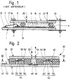
- Devices comprising several substrates, for example a flow collector provided with a chemical sensor such as a pH sensor, shown schematically in section in FIG. 1.
- a chemical sensor such as a pH sensor
- Such a collector comprises a first substrate 1 on one face 2 of which is fixed a sensor module 4 comprising for example a silicon plate on which is integrated a detection cell 6 comprising in particular measurement electrodes (not shown) connected respectively to pads 8 contact contacts. These are connected to contact pads 10 integral with the first substrate 1 by welding of wires 12, with a view to a connection with an external measurement circuit (not shown).
- the collector further comprises a second substrate 14 superimposed on the first substrate 1, an O-ring seal 16 being interposed between the two substrates 1 and 14 so that the contour of the seal 16 surrounds the area of the plate 4 comprising the detection cell 6.
- the plate 4, the O-ring 16 and the substrate 14 thus delimit a sealed collecting chamber 18 in which a fluid can circulate via an inlet channel 20 and a outlet channel 22 formed in the substrate 14 appropriately.
- the sealing of the chamber 18 vis-à-vis the other elements of the device is achieved by keeping the two substrates 1 and 14 tight against each other by means of a system of clamps 24 with screws or the like. .
- an O-ring seal has the disadvantage of making it difficult to achieve perfect sealing in cases where the surfaces of the device in contact with the seal are not smooth but more or less strongly structured. , which is the case with many detection cells.
- the main object of the invention is to remedy the drawbacks of the aforementioned prior art by providing a device comprising at least two substrates, intended to form a microsystem or part of a microsystem, which is easy and economical to implement. work and which allows, in the case of a device intended to convey a fluid, to effectively protect the elements of the device from the transported fluid while guaranteeing the desired tightness.
- the subject of the invention is a device comprising a first substrate and a second substrate intended to form a microsystem at least one of the substrates which may include electronic circuit elements, characterized in that a layer of polymer is interposed between the first and the second substrate, in that the polymer layer comprises at least one cavity which extends from the first to the second substrate and in that welding connection means are provided in the cavity, said means connection ensuring a mechanical connection resistant to traction between the two substrates.
- the bonding means by solder comprise solder pads provided respectively on each substrate and solder material connecting the solder pad of the first substrate to the solder pad of the second substrate.
- This mechanical assembly can thus also advantageously ensure an electrical and thermal connection between the substrates, respectively to, if necessary, return an electrical contact from one substrate to the other and to contribute to a more efficient dissipation of the heat produced. during operation of the device.
- the polymer layer is compressed between the first and the second substrate, and the weld is subjected to a permanent tensile force, the polymer being compressed between the two substrates.
- the polymer layer comprises a chamber intended to receive a fluid or a gas, formed in the polymer layer, the polymer of the layer ensuring the seal between the chamber and the cavity and / or outside.
- the polymer of the layer is a polymer belonging to the family of polysiloxanes.
- These polymers have the advantage of being able to undergo a double polymerization and thus of being able during the second polymerization to adhere to the substrates, thus increasing the tightness and the cohesion of the device.
- advantage is taken advantage of the structuring of the polymer layer to use the cavity or cavities as a mold for the formation of the pads to be welded, for example for the galvanic growth of a metal intended to form the beach to be welded.
- this layer of polymer makes it possible to produce seals having any shape and width as a function of the desired application.
- the drawing does not represent the exact relative dimensions of the elements with respect to each other and that the dimensions have been greatly exaggerated for the sake of clarity.
- the general dimensions of such a device are of the order of 10 x 10 x 1 mm 3 .
- the device 30 comprises a first substrate 32 and a second substrate 34 between which a layer of compressible polymer 36 is interposed.
- the substrates can be made of a semiconductor material such as silicon.
- the polymer layer 36 is preferably made from a polymer having photosensitive properties for reasons which will appear later and preferably which is part of the family of polysiloxanes.
- the polymer layer 36 comprises four cavities 38 extending between the respectively opposite faces 40 and 42 of the substrates 32 and 34, cavities in which are provided welding means 44 ensuring the mechanical connection between the substrates 32 and 34.
- the polymer layer 36 comprises, in the application illustrated in the figures, a collecting chamber 46 intended to receive a liquid or gaseous sample to be tested and in which a pH detection cell 48 is provided in the example illustrated.
- the detection cell 48 has for example a plurality of electrodes integrated on the substrate 34 and connected to contact pads 50 situated outside the chamber 46.
- This collecting chamber 46 is supplied via an inlet channel 52 provided in the substrate 32.
- the liquid or the gas, after coming into contact with the detection 48, is evacuated from the chamber 46 by an outlet channel 54.
- the soldering means 44 comprise pads to be welded 56, 58, formed respectively on the faces 40, 42 of the substrates 32 and 34 in the cavities 38, and of the material to be welded 60 which connects the pads to be welded 56 of the substrate 32 to solder pads 58 of substrate 34.
- the solder pads are made of metal and preferably these solder pads are made of nickel. Of course, any other metal capable of forming a mechanical bond between the substrate and the solder can be used.
- solder material 60 preferably a lead and tin solder alloy.
- the polymer layer 36 is compressed between the substrates 32 and 34 so that the solder connection 44 is subjected to a tensile force exerted by the compressed polymer.
- the polymer layer 36 is preferably integral with at least one of the substrates 32, 34.
- the assembly of the two substrates with the polymer layer is compressed and undergoes a rise in temperature to reach the temperature of the fusion of the soldering material, which makes it possible to carry out a second polymerization of the polymer simultaneously, during which a bond is created between the polymer layer and the substrates.
- the polymer layer 36 can, according to an alternative embodiment, be produced in the form of a sheet integral with any of the substrates and be prepared separately with an appropriate structure of the cavities.
- the structured sheet is simply kept compressed between the substrates by the bond by welding.
- the description and the figures will relate, for simplification, only to a single functional device.
- the process is preferably a "batch" process which allows a plurality of devices to be manufactured simultaneously on the same wafer.
- the plates forming the first and second substrates 32 and 34 from which the device or microsystem 30 is made are preferably made of a semiconductor material such as silicon.
- Figure 5 there is shown the first substrate 32 after the formation on the face 40 of the pads to be welded 56 and the deposit on these pads to be welded of the material to be welded 60, as well as the second substrate 34 after the formation of the layer 36 and pads to be welded 58.
- pads to be welded 56 is carried out conventionally by evaporation under vacuum of a metal, for example nickel or aluminum, through a mask (not shown).
- a metal for example nickel or aluminum
- these pads 56 and 58 can also be produced by any other means, for example by sputtering.
- the material to weld 60 is also deposited in the same way on the pads 56 through a mask.
- a layer of photosensitive polymer 36 has been deposited on its face 42, for example by spin spinning.
- the upper surface thus obtained is flat and smooth, which improves the seal during its application against the other substrate.
- the polymer layer conforms to the reliefs that the face of the substrate on which it is deposited could have.
- the polymer layer 36 was exposed through a mask (not shown) having an appropriate configuration. The exposed parts of the polymer layer 36 were then conventionally removed, for example by the wet method, to form the cavities 38 and the collecting chamber 46 until the surface 42 of the substrate 34 appeared.
- the polymer forming the layer 36 will preferably be a polysiloxane, this photosensitive polymer having good planarization properties and being capable of undergoing double polymerization thus giving it additional adhesion properties. Furthermore, this polymer has good compressibility.
- the next step consists in forming the pads 58 to be welded in the bottom of the cavities 38 which have just been formed in the layer 34.
- the cavities 38 are preferably used as molds for galvanically growing a metal. intended to form the pads 58.
- the metal used to form these pads 58 is preferably nickel.
- the substrates 32 and 34 are placed one on the other so that the pads to be welded 56 provided with the material to be welded 60 respectively penetrate into the corresponding cavities 28 formed in the polymer layer 34 and thus come opposite the corresponding pads to be welded 58.
- the two substrates 32 and 34 being thus prepared, they are placed in an aligner-welder (not shown) in which a sufficient pressure is applied to them to compress the layer 34 while being heated to a temperature sufficient to melt the solder material 60 and bond the solder pads 56 and 58 by soldering.
- an aligner-welder not shown
- all of the two substrates will be heated so that the solder material reaches a temperature of about 200 ° C.
- the thickness of the pads to be welded 58 is sufficient so that when the substrates 32 and 34 are superimposed and the polymer layer is compressed, the solder material comes into contact with the pad to be welded which it must connect.
- the pads to be welded connected to integrated electronic components of the substrate and the soldering means also ensure the return of an electrical contact from one substrate to the other.
- the device which has just been described finds applications in particular in the fields of fluidics, chemical or biological sensors, ink jet printer heads and the like.
Landscapes
- Chemical & Material Sciences (AREA)
- Life Sciences & Earth Sciences (AREA)
- Health & Medical Sciences (AREA)
- Physics & Mathematics (AREA)
- Chemical Kinetics & Catalysis (AREA)
- Electrochemistry (AREA)
- Molecular Biology (AREA)
- Analytical Chemistry (AREA)
- Biochemistry (AREA)
- General Health & Medical Sciences (AREA)
- General Physics & Mathematics (AREA)
- Immunology (AREA)
- Pathology (AREA)
- Micromachines (AREA)
Applications Claiming Priority (2)
| Application Number | Priority Date | Filing Date | Title |
|---|---|---|---|
| FR9605319A FR2748156B1 (fr) | 1996-04-26 | 1996-04-26 | Dispositif comprenant deux substrats destines a former un microsysteme ou une partie d'un microsysteme et procede d'assemblage de deux substrats micro-usines |
| FR9605319 | 1996-04-26 |
Publications (2)
| Publication Number | Publication Date |
|---|---|
| EP0803729A1 true EP0803729A1 (de) | 1997-10-29 |
| EP0803729B1 EP0803729B1 (de) | 2005-08-24 |
Family
ID=9491640
Family Applications (1)
| Application Number | Title | Priority Date | Filing Date |
|---|---|---|---|
| EP97106711A Expired - Lifetime EP0803729B1 (de) | 1996-04-26 | 1997-04-23 | Vorrichtung mit zwei mikromechanischen Substraten für ein mikromechanisches System oder Teil eines mikromechanischen Systems und Verfahren zur Zusammensetzung zweier mikromechanischer Substrate |
Country Status (4)
| Country | Link |
|---|---|
| US (1) | US6124631A (de) |
| EP (1) | EP0803729B1 (de) |
| DE (1) | DE69734039T2 (de) |
| FR (1) | FR2748156B1 (de) |
Families Citing this family (16)
| Publication number | Priority date | Publication date | Assignee | Title |
|---|---|---|---|---|
| JP3094948B2 (ja) * | 1997-05-26 | 2000-10-03 | 日本電気株式会社 | 半導体素子搭載用回路基板とその半導体素子との接続方法 |
| EP0951068A1 (de) | 1998-04-17 | 1999-10-20 | Interuniversitair Micro-Elektronica Centrum Vzw | Herstellungsverfahren für eine Mikrostruktur mit Innenraum |
| US7115986B2 (en) * | 2001-05-02 | 2006-10-03 | Micron Technology, Inc. | Flexible ball grid array chip scale packages |
| SG122743A1 (en) * | 2001-08-21 | 2006-06-29 | Micron Technology Inc | Microelectronic devices and methods of manufacture |
| DE10159860C2 (de) * | 2001-12-06 | 2003-12-04 | Sdk Technik Gmbh | Wärmeübertragungsfläche mit einer aufgalvanisierten Mikrostruktur von Vorsprüngen |
| SG104293A1 (en) | 2002-01-09 | 2004-06-21 | Micron Technology Inc | Elimination of rdl using tape base flip chip on flex for die stacking |
| SG121707A1 (en) | 2002-03-04 | 2006-05-26 | Micron Technology Inc | Method and apparatus for flip-chip packaging providing testing capability |
| US6975035B2 (en) * | 2002-03-04 | 2005-12-13 | Micron Technology, Inc. | Method and apparatus for dielectric filling of flip chip on interposer assembly |
| SG115459A1 (en) | 2002-03-04 | 2005-10-28 | Micron Technology Inc | Flip chip packaging using recessed interposer terminals |
| SG115455A1 (en) | 2002-03-04 | 2005-10-28 | Micron Technology Inc | Methods for assembly and packaging of flip chip configured dice with interposer |
| SG111935A1 (en) * | 2002-03-04 | 2005-06-29 | Micron Technology Inc | Interposer configured to reduce the profiles of semiconductor device assemblies and packages including the same and methods |
| SG115456A1 (en) | 2002-03-04 | 2005-10-28 | Micron Technology Inc | Semiconductor die packages with recessed interconnecting structures and methods for assembling the same |
| US20040036170A1 (en) | 2002-08-20 | 2004-02-26 | Lee Teck Kheng | Double bumping of flexible substrate for first and second level interconnects |
| US8487428B2 (en) * | 2007-11-20 | 2013-07-16 | Fujitsu Limited | Method and system for providing a reliable semiconductor assembly |
| US8039938B2 (en) | 2009-05-22 | 2011-10-18 | Palo Alto Research Center Incorporated | Airgap micro-spring interconnect with bonded underfill seal |
| US8558394B1 (en) * | 2012-08-29 | 2013-10-15 | Macronix International Co., Ltd. | Chip stack structure and manufacturing method thereof |
Citations (3)
| Publication number | Priority date | Publication date | Assignee | Title |
|---|---|---|---|---|
| EP0528251A2 (de) * | 1991-08-21 | 1993-02-24 | Honda Giken Kogyo Kabushiki Kaisha | Verfahren zur Herstellung eines Halbleitersensors der Gasströmung |
| EP0695941A2 (de) * | 1994-06-08 | 1996-02-07 | Affymax Technologies N.V. | Verfahren und Vorrichtung zum Verpacken von Chips |
| US5504035A (en) * | 1989-08-28 | 1996-04-02 | Lsi Logic Corporation | Process for solder ball interconnecting a semiconductor device to a substrate using a noble metal foil embedded interposer substrate |
Family Cites Families (19)
| Publication number | Priority date | Publication date | Assignee | Title |
|---|---|---|---|---|
| GB8304890D0 (en) * | 1983-02-22 | 1983-03-23 | Smiths Industries Plc | Chip-carrier substrates |
| US4893174A (en) * | 1985-07-08 | 1990-01-09 | Hitachi, Ltd. | High density integration of semiconductor circuit |
| JP2598328B2 (ja) * | 1989-10-17 | 1997-04-09 | 三菱電機株式会社 | 半導体装置およびその製造方法 |
| US5187020A (en) * | 1990-07-31 | 1993-02-16 | Texas Instruments Incorporated | Compliant contact pad |
| US5148266A (en) * | 1990-09-24 | 1992-09-15 | Ist Associates, Inc. | Semiconductor chip assemblies having interposer and flexible lead |
| US5279711A (en) * | 1991-07-01 | 1994-01-18 | International Business Machines Corporation | Chip attach and sealing method |
| US5202754A (en) * | 1991-09-13 | 1993-04-13 | International Business Machines Corporation | Three-dimensional multichip packages and methods of fabrication |
| US5767580A (en) * | 1993-04-30 | 1998-06-16 | Lsi Logic Corporation | Systems having shaped, self-aligning micro-bump structures |
| US5753972A (en) * | 1993-10-08 | 1998-05-19 | Stratedge Corporation | Microelectronics package |
| US5517344A (en) * | 1994-05-20 | 1996-05-14 | Prime View Hk Limited | System for protection of drive circuits formed on a substrate of a liquid crystal display |
| US5523628A (en) * | 1994-08-05 | 1996-06-04 | Hughes Aircraft Company | Apparatus and method for protecting metal bumped integrated circuit chips during processing and for providing mechanical support to interconnected chips |
| FR2726397B1 (fr) * | 1994-10-28 | 1996-11-22 | Commissariat Energie Atomique | Film conducteur anisotrope pour la microconnectique |
| JPH08293524A (ja) * | 1995-04-21 | 1996-11-05 | Toshiba Corp | 半導体装置およびその製造方法 |
| WO1996037913A1 (en) * | 1995-05-22 | 1996-11-28 | Hitachi Chemical Company, Ltd. | Semiconductor device having a semiconductor chip electrically connected to a wiring substrate |
| US5659203A (en) * | 1995-06-07 | 1997-08-19 | International Business Machines Corporation | Reworkable polymer chip encapsulant |
| JP3263288B2 (ja) * | 1995-09-13 | 2002-03-04 | 株式会社東芝 | 半導体装置 |
| US5796165A (en) * | 1996-03-19 | 1998-08-18 | Matsushita Electronics Corporation | High-frequency integrated circuit device having a multilayer structure |
| US5825092A (en) * | 1996-05-20 | 1998-10-20 | Harris Corporation | Integrated circuit with an air bridge having a lid |
| US5770477A (en) * | 1997-02-10 | 1998-06-23 | Delco Electronics Corporation | Flip chip-on-flip chip multi-chip module |
-
1996
- 1996-04-26 FR FR9605319A patent/FR2748156B1/fr not_active Expired - Fee Related
-
1997
- 1997-04-17 US US08/842,875 patent/US6124631A/en not_active Expired - Fee Related
- 1997-04-23 DE DE69734039T patent/DE69734039T2/de not_active Expired - Fee Related
- 1997-04-23 EP EP97106711A patent/EP0803729B1/de not_active Expired - Lifetime
Patent Citations (3)
| Publication number | Priority date | Publication date | Assignee | Title |
|---|---|---|---|---|
| US5504035A (en) * | 1989-08-28 | 1996-04-02 | Lsi Logic Corporation | Process for solder ball interconnecting a semiconductor device to a substrate using a noble metal foil embedded interposer substrate |
| EP0528251A2 (de) * | 1991-08-21 | 1993-02-24 | Honda Giken Kogyo Kabushiki Kaisha | Verfahren zur Herstellung eines Halbleitersensors der Gasströmung |
| EP0695941A2 (de) * | 1994-06-08 | 1996-02-07 | Affymax Technologies N.V. | Verfahren und Vorrichtung zum Verpacken von Chips |
Also Published As
| Publication number | Publication date |
|---|---|
| FR2748156B1 (fr) | 1998-08-07 |
| FR2748156A1 (fr) | 1997-10-31 |
| US6124631A (en) | 2000-09-26 |
| DE69734039D1 (de) | 2005-09-29 |
| DE69734039T2 (de) | 2006-06-29 |
| EP0803729B1 (de) | 2005-08-24 |
Similar Documents
| Publication | Publication Date | Title |
|---|---|---|
| EP0803729B1 (de) | Vorrichtung mit zwei mikromechanischen Substraten für ein mikromechanisches System oder Teil eines mikromechanischen Systems und Verfahren zur Zusammensetzung zweier mikromechanischer Substrate | |
| WO1999067818A1 (fr) | Dispositif et procede de formation d'un dispositif presentant une cavite a atmosphere controlee | |
| EP1093159A1 (de) | Verfahren zum Einkapseln von elektronischen Komponenten | |
| FR2697675A1 (fr) | Procédé de fabrication de transducteurs capacitifs intégrés. | |
| FR2874088A1 (fr) | Capteur de pression | |
| EP1586122B1 (de) | Photovoltaisches modul mit aussenanschlussklemmen | |
| WO2000033044A1 (fr) | Capteur de pression a membrane comportant du carbure de silicium et procede de fabrication | |
| EP0336859A1 (de) | Piezoelektrische Kapsel mit lateralen elektrischen Verbindungszangen | |
| FR2791430A1 (fr) | Capteur de pression a tige metallique fixee a un boitier pouvant etre assujetti directement a un dispositif, et procede pour fabriquer celui-ci | |
| EP1919822A1 (de) | Verfahren zum miteinander versiegeln oder verschweissen von zwei elementen | |
| EP2236864B1 (de) | Metalllippendichtung und mit einer solchen Dichtung ausgestattete Maschine | |
| FR2643753A1 (fr) | Procede d'interconnexion de composants electriques au moyen d'elements conducteurs, deformables et sensiblement spheriques | |
| EP0639761A1 (de) | Kapazitiver Differenzdruckwandler | |
| EP1824779B1 (de) | Vorrichtung und verfahren zur hermetischen abdichtung eines hohlraums in einem elektronischen bauteil | |
| FR2747841A1 (fr) | Procede de fabrication d'elements semi-conducteurs presentant des structures micromecaniques | |
| EP1427008B1 (de) | Herstellungsverfahren für einen elektronischen Modul mit einem aktiven Bauteil auf einem Substrat | |
| EP2636064B1 (de) | Verbindungselemente zur herstellung von elektronischen hybridschaltungen | |
| FR2594286A1 (fr) | Procede d'interconnexion electrique et mecanique de deux corps, notamment dans un capteur de pression | |
| WO2009053398A1 (fr) | Architecture de pile a combustible integre sans joint. | |
| EP3971133B1 (de) | Verfahren zur herstellung einer mikrofluidischen vorrichtung und mit diesem verfahren erhaltene vorrichtung | |
| FR2859045A1 (fr) | Dispositif de connexion electrique entre deux plaquettes et procede de realisation d'un composant microelectronique comportant un tel dispositif | |
| FR2857504A1 (fr) | Capteur d'image de grande dimension et procede de fabrication | |
| EP2519087B1 (de) | Einkapselungshülle für ein System mit elektrischen Verbindungen, Herstellungsverfahren dergleichen, mit einer solchen Hülle versehenes eingekapseltes System und Stapeln solcher Systeme | |
| FR2722878A1 (fr) | Capteur de pression differentielle de type capacitif | |
| FR2741010A1 (fr) | Carte comprenant une unite electronique et procede de fabrication d'une telle carte |
Legal Events
| Date | Code | Title | Description |
|---|---|---|---|
| PUAI | Public reference made under article 153(3) epc to a published international application that has entered the european phase |
Free format text: ORIGINAL CODE: 0009012 |
|
| AK | Designated contracting states |
Kind code of ref document: A1 Designated state(s): CH DE FR GB LI NL |
|
| RIN1 | Information on inventor provided before grant (corrected) |
Inventor name: VAN DER SCHOOT,BART Inventor name: ARQUINT,PHILIPPE Inventor name: CARDOT, FRANCIS |
|
| 17P | Request for examination filed |
Effective date: 19980429 |
|
| RAP1 | Party data changed (applicant data changed or rights of an application transferred) |
Owner name: COLIBRYS S.A. |
|
| 17Q | First examination report despatched |
Effective date: 20020213 |
|
| GRAP | Despatch of communication of intention to grant a patent |
Free format text: ORIGINAL CODE: EPIDOSNIGR1 |
|
| GRAS | Grant fee paid |
Free format text: ORIGINAL CODE: EPIDOSNIGR3 |
|
| GRAA | (expected) grant |
Free format text: ORIGINAL CODE: 0009210 |
|
| AK | Designated contracting states |
Kind code of ref document: B1 Designated state(s): CH DE FR GB LI NL |
|
| PG25 | Lapsed in a contracting state [announced via postgrant information from national office to epo] |
Ref country code: NL Free format text: LAPSE BECAUSE OF FAILURE TO SUBMIT A TRANSLATION OF THE DESCRIPTION OR TO PAY THE FEE WITHIN THE PRESCRIBED TIME-LIMIT Effective date: 20050824 |
|
| REG | Reference to a national code |
Ref country code: GB Ref legal event code: FG4D Free format text: NOT ENGLISH |
|
| REG | Reference to a national code |
Ref country code: CH Ref legal event code: EP |
|
| REF | Corresponds to: |
Ref document number: 69734039 Country of ref document: DE Date of ref document: 20050929 Kind code of ref document: P |
|
| REG | Reference to a national code |
Ref country code: CH Ref legal event code: NV Representative=s name: PATENTS & TECHNOLOGY SURVEYS SA |
|
| GBT | Gb: translation of ep patent filed (gb section 77(6)(a)/1977) |
Effective date: 20051201 |
|
| NLV1 | Nl: lapsed or annulled due to failure to fulfill the requirements of art. 29p and 29m of the patents act | ||
| PLBE | No opposition filed within time limit |
Free format text: ORIGINAL CODE: 0009261 |
|
| STAA | Information on the status of an ep patent application or granted ep patent |
Free format text: STATUS: NO OPPOSITION FILED WITHIN TIME LIMIT |
|
| 26N | No opposition filed |
Effective date: 20060526 |
|
| PGFP | Annual fee paid to national office [announced via postgrant information from national office to epo] |
Ref country code: FR Payment date: 20090414 Year of fee payment: 13 Ref country code: DE Payment date: 20090422 Year of fee payment: 13 |
|
| PGFP | Annual fee paid to national office [announced via postgrant information from national office to epo] |
Ref country code: CH Payment date: 20090417 Year of fee payment: 13 |
|
| PGFP | Annual fee paid to national office [announced via postgrant information from national office to epo] |
Ref country code: GB Payment date: 20090421 Year of fee payment: 13 |
|
| REG | Reference to a national code |
Ref country code: CH Ref legal event code: PL |
|
| GBPC | Gb: european patent ceased through non-payment of renewal fee |
Effective date: 20100423 |
|
| REG | Reference to a national code |
Ref country code: FR Ref legal event code: ST Effective date: 20101230 |
|
| PG25 | Lapsed in a contracting state [announced via postgrant information from national office to epo] |
Ref country code: LI Free format text: LAPSE BECAUSE OF NON-PAYMENT OF DUE FEES Effective date: 20100430 Ref country code: DE Free format text: LAPSE BECAUSE OF NON-PAYMENT OF DUE FEES Effective date: 20101103 Ref country code: CH Free format text: LAPSE BECAUSE OF NON-PAYMENT OF DUE FEES Effective date: 20100430 |
|
| PG25 | Lapsed in a contracting state [announced via postgrant information from national office to epo] |
Ref country code: GB Free format text: LAPSE BECAUSE OF NON-PAYMENT OF DUE FEES Effective date: 20100423 |
|
| PG25 | Lapsed in a contracting state [announced via postgrant information from national office to epo] |
Ref country code: FR Free format text: LAPSE BECAUSE OF NON-PAYMENT OF DUE FEES Effective date: 20100430 |