EP0782202A2 - Epitaktischer Verbindungshalbleiterwafer - Google Patents
Epitaktischer Verbindungshalbleiterwafer Download PDFInfo
- Publication number
- EP0782202A2 EP0782202A2 EP96309407A EP96309407A EP0782202A2 EP 0782202 A2 EP0782202 A2 EP 0782202A2 EP 96309407 A EP96309407 A EP 96309407A EP 96309407 A EP96309407 A EP 96309407A EP 0782202 A2 EP0782202 A2 EP 0782202A2
- Authority
- EP
- European Patent Office
- Prior art keywords
- layer
- nitrogen
- gallium phosphide
- carrier concentration
- type carrier
- Prior art date
- Legal status (The legal status is an assumption and is not a legal conclusion. Google has not performed a legal analysis and makes no representation as to the accuracy of the status listed.)
- Withdrawn
Links
Images



Classifications
-
- H—ELECTRICITY
- H10—SEMICONDUCTOR DEVICES; ELECTRIC SOLID-STATE DEVICES NOT OTHERWISE PROVIDED FOR
- H10P—GENERIC PROCESSES OR APPARATUS FOR THE MANUFACTURE OR TREATMENT OF DEVICES COVERED BY CLASS H10
- H10P14/00—Formation of materials, e.g. in the shape of layers or pillars
- H10P14/20—Formation of materials, e.g. in the shape of layers or pillars of semiconductor materials
-
- H—ELECTRICITY
- H10—SEMICONDUCTOR DEVICES; ELECTRIC SOLID-STATE DEVICES NOT OTHERWISE PROVIDED FOR
- H10H—INORGANIC LIGHT-EMITTING SEMICONDUCTOR DEVICES HAVING POTENTIAL BARRIERS
- H10H20/00—Individual inorganic light-emitting semiconductor devices having potential barriers, e.g. light-emitting diodes [LED]
- H10H20/80—Constructional details
- H10H20/81—Bodies
- H10H20/822—Materials of the light-emitting regions
- H10H20/824—Materials of the light-emitting regions comprising only Group III-V materials, e.g. GaP
- H10H20/8242—Materials of the light-emitting regions comprising only Group III-V materials, e.g. GaP characterised by the dopants
-
- H—ELECTRICITY
- H10—SEMICONDUCTOR DEVICES; ELECTRIC SOLID-STATE DEVICES NOT OTHERWISE PROVIDED FOR
- H10H—INORGANIC LIGHT-EMITTING SEMICONDUCTOR DEVICES HAVING POTENTIAL BARRIERS
- H10H20/00—Individual inorganic light-emitting semiconductor devices having potential barriers, e.g. light-emitting diodes [LED]
- H10H20/80—Constructional details
- H10H20/81—Bodies
- H10H20/8215—Bodies characterised by crystalline imperfections, e.g. dislocations; characterised by the distribution of dopants, e.g. delta-doping
-
- H—ELECTRICITY
- H10—SEMICONDUCTOR DEVICES; ELECTRIC SOLID-STATE DEVICES NOT OTHERWISE PROVIDED FOR
- H10P—GENERIC PROCESSES OR APPARATUS FOR THE MANUFACTURE OR TREATMENT OF DEVICES COVERED BY CLASS H10
- H10P14/00—Formation of materials, e.g. in the shape of layers or pillars
- H10P14/20—Formation of materials, e.g. in the shape of layers or pillars of semiconductor materials
- H10P14/34—Deposited materials, e.g. layers
- H10P14/3402—Deposited materials, e.g. layers characterised by the chemical composition
- H10P14/3414—Deposited materials, e.g. layers characterised by the chemical composition being group IIIA-VIA materials
- H10P14/3418—Phosphides
-
- H—ELECTRICITY
- H10—SEMICONDUCTOR DEVICES; ELECTRIC SOLID-STATE DEVICES NOT OTHERWISE PROVIDED FOR
- H10P—GENERIC PROCESSES OR APPARATUS FOR THE MANUFACTURE OR TREATMENT OF DEVICES COVERED BY CLASS H10
- H10P14/00—Formation of materials, e.g. in the shape of layers or pillars
- H10P14/20—Formation of materials, e.g. in the shape of layers or pillars of semiconductor materials
- H10P14/34—Deposited materials, e.g. layers
- H10P14/3402—Deposited materials, e.g. layers characterised by the chemical composition
- H10P14/3414—Deposited materials, e.g. layers characterised by the chemical composition being group IIIA-VIA materials
- H10P14/3421—Arsenides
Definitions
- the present invention relates to a compound semiconductor epitaxial wafer, in particular to a compound semiconductor epitaxial wafer having a gallium phosphide arsenide mixed-crystalline epitaxial layer added with nitrogen.
- Conventional indirect transition III-V compound light-emitting diodes producing most popularly red light but also yielding orange or yellow lights, in particular those based on gallium phosphide arsenide GaAs 1-x P x (where, 0.45 ⁇ x ⁇ 1.0) employ an epitaxial wafer in which a GaAs 1-x P x epitaxial layer is grown on a gallium phosphide GaP or gallium arsenide GaAs single-crystalline substrate, and an uppermost area of the epitaxial layer is doped through diffusion of p-type impurity to form a p-n junction, operating as a light emitting region.
- n-Type carrier concentration is referred as one major factor affecting the luminous efficiency, which has conventionally been set at 1 ⁇ 10 15 /cm 3 or above.
- n-type carrier concentration being limited within a range of 3.5 ⁇ 10 15 /cm 3 to 8.8 ⁇ 10 15 /cm 3 both inclusive.
- n-type carrier concentration has been set to 1 ⁇ 10 15 /cm 3 or above is that lowering carrier concentration of n-type epitaxial layer is difficult, and that most attempt to lower the concentration beyond that level would often result in an extremely low carrier concentration.
- an n-type carrier concentration to an appropriate range for an area or around where a p-n junction (referred as a p-n junction formation area, hereinafter) is formed by a diffusion of a p-type impurity from the uppermost surface of the n-type epitaxial layer.
- n-type carrier concentration a concentration of n-type carrier in the vicinity of the p-n junction formation area, for example, causes an unstable luminance level due to low crystal quality and a lowered luminance due to increased absorption of the light
- the n-type carrier concentration becomes extremely low, on the contrary, opportunities of recombination of electrons and holes become fewer and causes a lowered emission output and a higher forward voltage Vf.
- Nitrogen concentration is referred as another factor known to govern the luminous efficiency. Since a light emitting diode using indirect III-V semiconductor results in inefficient emission with a p-n junction alone, general applicaion adds nitrogen acting as an emission center called as an isoelectronic trap in the emission region to improve the efficiency. It is thus said that the concentration of nitrogen added as an isoelectronic trap, as well as n-type carrier concentration, are critical factors affecting luminance, wavelength and other emission characteristics.
- the inventors of the present invention having devotedly been investigating into the distribution of n-type carrier concentration in the direction of the thickness of nitrogen-added gallium phosphide arsenide mixed crystalline epitaxial layer, and into optimizating combination of n-type carrier and nitrogen concentrations, which have reached compound semiconductor epitaxial wafer composed as mentioned below.
- the above object is attained by providing a compound semiconductor epitaxial wafer having a single crystalline substrate made of gallium phosphide or gallium arsenide and epitaxial layers grown on its surface, in which the epitaxial layers have at least a nitrogen-added gallium phosphide arsenide mixed crystalline epitaxial layer, whose n-type carrier concentration before being diffused with p-type impurity is descending toward the uppermost surface of the grown layer in a continuous or stepwise manner.
- the gallium phosphide arsenide mixed crystalline epitaxial layers have in the vicinity of p-n junction formation area an intermediate layer with a n-type carrier concentration ranging from 4 ⁇ 10 14 /cm 3 to 3.5 ⁇ 10 15 /cm 3 , the lower end inclusive, and a surface layer having a n-type carrier concentration equals to or lower than that of the intermediate layer.
- a more preferable range for n-type carrier is from 4 ⁇ 10 14 /cm 3 to 1.0 ⁇ 10 1 5 /cm 3 , the lower end inclusive, for the intermediate layer, and more lower for the surface layer.
- Thickness of the intermediate layer preferably ranges from 7 to 15 ⁇ m, both inclusive.
- a preferable range of thickness of the surface layer is from 2 to 5 ⁇ m.
- a compound semiconductor epitaxial wafer of the present invention it is preferable to reduce carrier concentration in the nitrogen-added gallium phosphide arsenide mixed crystalline epitaxial layer toward the uppermost surface of the grown layer in a continuous or stepwise manner, which results in improved crystallinity in the vicinity of the p-n junction formation area, improved emission characteristics due to reduced loss ascribable to light absorption, and prevention of increasing trends in forward voltage Vf.
- the emission characteristics can further be improved by optimizing a combination of n-type carrier concentration and that for nitrogen acts as an isoelectronic trap.
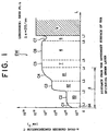
- Fig.1 shows a graphical representation of the distribution of n-type carrier concentration along with the direction of the film thickness as plotted against the distance from the uppermost surface of the epitaxially grown layer on a compound semiconductor epitaxial wafer in accordance with a first embodiment of the invention.
- Fig.2 shows a schematic sectional view for explaining a constitution of the compound semiconductor epitaxial wafer shown in Fig.1.
- a compound semiconductor epitaxial wafer EW of the invention comprises a gallium phosphide single crystal substrate 4, a gallium phosphide epitaxial layer 5 being grown on the substrate 4, a gallium phosphide arsenide GaAs 1-x P x crystal mixing ratio gradient layer 6 with its crystal mixing ratio gradually varied in the direction of the layer growth, being grown on the epitaxial layer 5, a gallium phosphide arsenide GaAs 1-a P a composition-constant layer 7, with its crystal mixing ratio "a" kept constant being layered on the crystal mixing ratio gradient layer 6, and a gallium phosphide arsenide GaAs 1-a P a epitaxial layer 8 added with nitrogen being formed on the composition-constant layer 7.
- the nitrogen-added epitaxial layer 8 further comprises in this order a nitrogen concentration adjusting layer 81 for gradually adjusting the concentration of nitrogen to be added being formed adjacent to the composition-constant layer 7, a steady layer 82 having a constant nitrogen concentration, a intermediate layer 83 which provides a p-n junction area and occupies its n-type area, and a surface layer 84 where p-type impurity to be diffused.
- a light emitting diode is finished after diffusing p-type impurity from the uppermost area of the surface layer 84 into the hetero-structured epitaxial wafer EW mentioned above, bonding electrodes, dicing to an appropriate size, and enclosing into a package.
- gallium phosphide GaP used as a single crystal substrate will also apply to the case that gallium arsenide GaAs is used instead.
- Distance L7-L6 from the uppermost surface of the epitaxial grown layer corresponds to the gallium phosphide GaP layer 5 with a thickness of 4 ⁇ m, within which carrier concentration c7 is so given that starting from 5 ⁇ 10 17 /cm 3 , which equals to an n-type carrier concentration of the single crystal substrate 4, decreasing to 1 ⁇ 10 17 /cm 3 , and then being partially recovered to 3 ⁇ 10 17 /cm 3 .
- distances L6-L5 and L5-L4 correspond to the gallium phosphide arsenide GaAs 1-x P x crystal mixing ratio gradient layer 6 and gallium phosphide arsenide GaAs 1-a P a composition constant layer 7, respectively.
- carrier concentrations c6, c5 are almost constant at 3 ⁇ 10 17 /cm 3 for both of them.
- An area between distance L4 and the uppermost surface of the epitaxial layer corresponds to the nitrogen-added epitaxial layer 8.
- the nitrogen concentration adjusting layer 81 occupying the lowest part of the layer 8 is formed between distances L4 and L3 into 4- ⁇ m thick with a carrier concentration c4 descended from 3 ⁇ 10 17 /cm 3 to 3 ⁇ 10 16 /cm 3 toward the uppermost surface of the grown layer.
- the steady layer 82 of 4 ⁇ m-thick corresponded to the area between distances L3 and L2 has a carrier concentration c3 almost constant at 3 ⁇ 10 16 /cm 3 as continued from the lower end of carrier concentration c4, the intermediate layer 83 of 8 ⁇ m-thick corresponded to the area between distances L2 and L1 has a carrier concentration c2 as maintained almost as plateau after a sharp drop from carrier concentration c3 to 8 ⁇ 10 14 /cm 3 ), and the surface layer 84 of of 4 ⁇ m-thick corresponded to the area between distance L1 and the uppermost surface has a carrier concentration c1 as gradually decreased from carrier concentration c2 to 5 ⁇ 10 14 /cm 3 along the direction of the layer growth.
- n-type carrier concentration gradually decreases in continuous and step-wise manners over the range from the nitrogen concentration adjusting layer 81 to the surface layer 84.
- n-Type carrier concentration is preferably selected in a range of 1 ⁇ 10 16 to 50 ⁇ 10 16 /cm 3 for the area between the gallium phosphide GaP epitaxial layer 5 and the steady layer 82, in a range of 4 ⁇ 10 14 to 35 ⁇ 10 14 /cm 3 for the intermediate layer 83, and at a concentration not higher than that of the intermediate layer 83 for the surface layer 84, for all the ranges both marginal values inclusive.
- Fig. 6 shows a diagram of relations between n-type carrier concentration and emission luminance for the nitrogen-added intermediate layer 83 to which nitrogen is added to adjust ⁇ within a range from 150 to 250/cm both inclusive.
- an n-type carrier concentration equals to or exceeding 3.5 ⁇ 10 15 /cm 3 degrades the crystal uniformity to make the luminance level unstable, and the degraded crystal quality and associated increase in absorptivity of light will cause emission luminance to be lowered.
- n-type carrier concentration of 4 ⁇ 10 14 /cm 3 or below, on the contrary, will lead to reduction in the number of electron, which will lessen opportunities for electron-hole recombination to cause lowered emission output and higher forward voltage Vf.
- a most eminent luminance is obtained when the n-type carrier concentration of the intermediate layer 83 equals to or higher than 4 ⁇ 10 14 /cm 3 and lower than 1 ⁇ 10 15 /cm 3 .
- the nitrogen added epitaxial layer 8 it is more preferable to choose a layer thickness between 18 and 30 ⁇ m for the nitrogen added epitaxial layer 8, within which the steady layer 82 is favorably set to 1 ⁇ m or above, the intermediate layer 83 set to 7 to 15 ⁇ m and the surface layer 84 set to 2 to 5 ⁇ m, with all marginal values inclusive.
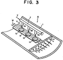
- FIG. 3 shows a perspective view of a production apparatus R of a compound semiconductor epitaxial wafer of the invention.
- This apparatus R comprises a lengthy boat 15 with its lefthand side being directed to upstream and the righthand side to downstream in this figure, and a gas feeding pipe 2 extended over the boat 15, equipped on which are gas discharge nozzles 2A, 2B and 2C aligned in this order from the upstream to the downstream.
- group V source gas V such as arsine or phosphine is supplied into the production apparatus R.
- a vessel of the production apparatus containing the boat 15 and the gas feeding pipe 2 are not shown in this figure.
- the boat 15 On the boat 15, a plurality of substrate is loaded from the upperstream to downstream and exposed to the group V souce gas V discharged downward from the gas discharge nozzles 2A, 2B and 2C.
- the group III source gas W mainly composed of gallium is separately supplied from the upstream of the boat 15 toward the downstream.
- the epitaxial wafer production appratus R described above allows the group V source gas to flow alone and be delivered close to each substrate 13 through the pipe and dispersively supplied, thus enabling the n-type carrier concentration to be controlled to 1 ⁇ 10 15 /cm 3 or below, such a low level hardly being controlled by the conventional appararus.
- the conventional constitution based on batch supply of source gases has been suffering from erosion of quartz-made reaction tube 1 at around the portion close to the inlet of the source gases where exposure of the reaction tube 1 to high concentration source gases would occur.
- Silicon released from the reaction tube as the result will be incorporated into the wafer together with dopants supplied into the reaction tube 1 to operate as an n-type carrier. It is thus contemplated that the past failure in controlling the carrier concentration at 1 ⁇ 10 15 /cm 3 or below is ascribable to fluctuation in the amount of silicon, released due to erosion of the reaction tube 1, from 7 ⁇ 10 14 to 30 ⁇ 10 14 /cm 3 .
- each gas discharge nozzle dispersively supplies the group V source gas V at a concentration only one-third to one-fourth of that in the conventional appratus, resulted in the source gas not being concentrated at a portion, so that the quartz-made reaction tube can almost exempt from erosion and thus hardly supply silicon, a possible n-type carrier.
- n-Type carrier concentration thus enabled to be controlled at 1 ⁇ 10 15 /cm 3 or below.
- Still another important merit of the above epitaxial wafer production apparatus R relates to precise control of flow rate, that is supply volume, of, in particular, the group V source gas V, which enables control for epitaxial film thickness, and precise control for carrier concentration and crystal mixing ratio in each layer.
- the above epitaxial wafer production apparatus R further employs a shielding plate 3 in the downstream of the boat 15 to prevent inverse diffusion of impurities from the exhaust portion of the reaction tube 1.
- this appratus is conveniently used for producing a compound semiconductor epitaxial wafer of the invention.
- the group III source gas W and the group V source gas V are flowed separately toward single crystal substrates 4 with supply volume of the group V gas being precisely controlled in particular, to grow the gallium phosphide GaP epitaxial layer 5, the gallium phosphide arsenide GaAs 1-x P x crystal mixing ratio gradient layer 6 with its crystal mixing ratio being varied gradually in the direction of the layer growth, and the gallium phosphide arsenide GaAs 1-a P a composition-constant layer 7 with constant crystal mixing ratio "a".
- a nitrogen concentration adjusting layer 81, a steady layer 82, an intermediate layer 83 and a surface layer 84 were grown adjacent to each other in this order to compose a nitrogen-added epitaxial layer 8, during which n-type dopant gas was supplied in a continuously or stepwisely reducing manner over the growth period from the steady layer 82 to the intermediate layer 83, and the n-type dopant gas was stopped for the growth period of the surface layer 84.
- Fig. 4 shows an example of changes in flow rate for supplying dopant gas according to the growth period of the epitaxial layer.
- Hydrogen sulfide H 2 S as an n-type dopant gas was diluted to 50 ppm with hydrogen gas H 2 then supplied at 190 cm 3 /min for 140 min during a period from starting the growth of the epitaxial layer to completion of the formation of the composition constant layer 7, at 7 cm 3 /min for 60 min during the formation of the nitrogen concentration adjusting layer 81 and the steady layer 82, at 1 cm 3 /min for 60 min during the formation of the intermediate layer 83, whereas the gas supply was discontinued for 30 min during the formation of the surface layer 84.
- an n-type carrier concentration in the nitrogen-added epitaxial layer 8 is provided so that it descends continuously and stepwisely toward the uppermost surface of the surface layer 84. This leads to improved crystallinity in the vicinity of the p-n junction formation area and, as a consequence, improved emisson characteristics. Forward voltage Vf was also prevented from being increased since n-type carrier concentration toward the substrate side is gradually increased to prevent n-type carrier concentration from becoming too low.
- nitrogen concentration as optimally combined with the n-type carrier concentration as mentioned above can be determined according to the ⁇ method based on differences in absorption coefficient.
- the ⁇ method is referred as a method for measuring the concentration of nitrogen added as an isoelectronic trap in indirect transition compound semiconductor (Japanese Patent Application No.55509 in 1995), in which light having a wavelength equals to or almost equals to an absorption wavelength ⁇ N ascribable to an exciton bound to an isoelectronic trap is employed as an incident light, an absorption coefficient ⁇ N of the nitrogen-added compound semiconductor for the incident light is subtracted by an absorption coefficient ⁇ of the nitrogen-free compound semiconductor to give difference ⁇ , then the nitrogen concentration is determined from known correlation between ⁇ and nitrogen concentration in compound semiconductor.
- the concentration of nitrogen added as an isoelectronic trap in the nitrogen-added epitaxial layer 8 is obtained in a nondestructive, accurate and facilitated manner by making reference to a previously obtained correlation of light absorption coefficient with ⁇ and ⁇ N . It has also been confirmed that there is an excellent correlation between ⁇ and nitrogen concentration determiened by SIMS.
- Fig. 5 shows a relationship between luminance and ⁇ for a compound semiconductor epitaxial wafer thus prepared by the invention having a carrier concentration of 6 ⁇ 10 14 to 10 ⁇ 10 14 /cm 3 .
- ⁇ is defined as representing difference between an absorption coefficient ⁇ of nitrogen-free compound semiconductor and an absorption coefficient ⁇ N of nitrogen-added indirect transition III-V compound semiconductor
- favorable luminance is attainable for ⁇ ranging from 100 to 300/cm (both ends inclusive) as known from Fig. 5.
- the best performance is obtained for ⁇ ranging more preferably from 150 to 250/cm (both ends inclusive).
- a compound seminconductor epitaxial wafer is constructed so that the combination of carrier concentration in the p-n junction forming area and corresponding nitrogen concentration is optimized, which allows full utilization of its emission properties and exerts a special merit in achieving high emission luminance.
- n-type carrier concentration in the nitrogen-added epitaxial layer is set properly low and gradually descending toward the uppermost surface of the surface layer, crystal uniformity is improved to stabilize luminance level, and to save the loss caused by light reabsorption. Further merits include stabilized processes and improved yield ratio.
Landscapes
- Led Devices (AREA)
- Recrystallisation Techniques (AREA)
- Chemical Vapour Deposition (AREA)
Applications Claiming Priority (2)
| Application Number | Priority Date | Filing Date | Title |
|---|---|---|---|
| JP352990/95 | 1995-12-27 | ||
| JP35299095A JP3355901B2 (ja) | 1995-12-27 | 1995-12-27 | 化合物半導体エピタキシャルウエーハ |
Publications (2)
| Publication Number | Publication Date |
|---|---|
| EP0782202A2 true EP0782202A2 (de) | 1997-07-02 |
| EP0782202A3 EP0782202A3 (de) | 1998-04-22 |
Family
ID=18427827
Family Applications (1)
| Application Number | Title | Priority Date | Filing Date |
|---|---|---|---|
| EP96309407A Withdrawn EP0782202A3 (de) | 1995-12-27 | 1996-12-23 | Epitaktischer Verbindungshalbleiterwafer |
Country Status (5)
| Country | Link |
|---|---|
| US (1) | US5912476A (de) |
| EP (1) | EP0782202A3 (de) |
| JP (1) | JP3355901B2 (de) |
| KR (1) | KR100273925B1 (de) |
| TW (1) | TW337619B (de) |
Cited By (1)
| Publication number | Priority date | Publication date | Assignee | Title |
|---|---|---|---|---|
| EP0954035A1 (de) * | 1998-04-30 | 1999-11-03 | Shin-Etsu Handotai Company Limited | Epitaxialscheibe und lichtemittierende Diode |
Families Citing this family (7)
| Publication number | Priority date | Publication date | Assignee | Title |
|---|---|---|---|---|
| JPH1154442A (ja) * | 1997-08-07 | 1999-02-26 | Shin Etsu Handotai Co Ltd | 化合物半導体エピタキシャルウェーハの製造方法およびこれに用いる気相成長装置 |
| JP3791672B2 (ja) * | 2001-04-27 | 2006-06-28 | 信越半導体株式会社 | 発光素子及びその製造方法 |
| US8562738B2 (en) | 2004-03-11 | 2013-10-22 | Epistar Corporation | Nitride-based light-emitting device |
| US9524869B2 (en) | 2004-03-11 | 2016-12-20 | Epistar Corporation | Nitride-based semiconductor light-emitting device |
| US7928424B2 (en) * | 2004-03-11 | 2011-04-19 | Epistar Corporation | Nitride-based light-emitting device |
| JP7351241B2 (ja) * | 2020-03-02 | 2023-09-27 | 信越半導体株式会社 | 化合物半導体エピタキシャルウェーハ及びその製造方法 |
| JP2021182615A (ja) * | 2020-05-15 | 2021-11-25 | 信越半導体株式会社 | 化合物半導体エピタキシャルウェーハ及びその製造方法 |
Family Cites Families (9)
| Publication number | Priority date | Publication date | Assignee | Title |
|---|---|---|---|---|
| US3725249A (en) * | 1971-12-14 | 1973-04-03 | Universal Oil Prod Co | Continuous reforming-regeneration process |
| JPS581539B2 (ja) * | 1978-07-07 | 1983-01-11 | 三菱化成ポリテック株式会社 | エピタキシヤルウエハ− |
| US4354140A (en) * | 1979-05-28 | 1982-10-12 | Zaidan Hojin Handotai Kenkyu Shinkokai | Light-emitting semiconductor |
| JPS571239A (en) * | 1980-06-02 | 1982-01-06 | Toshiba Corp | Evaluating device for single crystal of semiconductor |
| JPS60214524A (ja) * | 1984-04-10 | 1985-10-26 | Shin Etsu Handotai Co Ltd | 燐化砒化ガリウムエピタキシヤル膜の成長方法 |
| JPS60216537A (ja) * | 1984-04-11 | 1985-10-30 | Shin Etsu Handotai Co Ltd | 化合物半導体単結晶エピタキシヤル膜の気相成長法 |
| JPS61172031A (ja) * | 1986-01-09 | 1986-08-02 | Agency Of Ind Science & Technol | 硝酸態窒素と亜硝酸態窒素の合量を測定する方法 |
| JP3436379B2 (ja) * | 1992-07-28 | 2003-08-11 | 三菱化学株式会社 | りん化ひ化ガリウムエピタキシャルウエハ |
| JP3187213B2 (ja) * | 1993-08-25 | 2001-07-11 | 沖電気工業株式会社 | 受発光ダイオード |
-
1995
- 1995-12-27 JP JP35299095A patent/JP3355901B2/ja not_active Expired - Fee Related
-
1996
- 1996-12-20 US US08/770,500 patent/US5912476A/en not_active Expired - Fee Related
- 1996-12-23 EP EP96309407A patent/EP0782202A3/de not_active Withdrawn
- 1996-12-27 KR KR1019960073463A patent/KR100273925B1/ko not_active Expired - Fee Related
-
1997
- 1997-03-28 TW TW086103997A patent/TW337619B/zh not_active IP Right Cessation
Cited By (2)
| Publication number | Priority date | Publication date | Assignee | Title |
|---|---|---|---|---|
| EP0954035A1 (de) * | 1998-04-30 | 1999-11-03 | Shin-Etsu Handotai Company Limited | Epitaxialscheibe und lichtemittierende Diode |
| US6433365B1 (en) | 1998-04-30 | 2002-08-13 | Shin-Etsu Handotai Co., Ltd. | Epitaxial wafer and light emitting diode |
Also Published As
| Publication number | Publication date |
|---|---|
| JP3355901B2 (ja) | 2002-12-09 |
| JPH09186361A (ja) | 1997-07-15 |
| EP0782202A3 (de) | 1998-04-22 |
| TW337619B (en) | 1998-08-01 |
| KR970052054A (ko) | 1997-07-29 |
| US5912476A (en) | 1999-06-15 |
| KR100273925B1 (ko) | 2001-01-15 |
Similar Documents
| Publication | Publication Date | Title |
|---|---|---|
| US7998773B2 (en) | Method of growing semiconductor heterostructures based on gallium nitride | |
| US6110757A (en) | Method of forming epitaxial wafer for light-emitting device including an active layer having a two-phase structure | |
| KR100406201B1 (ko) | 이중 헤테로 구조체를 구비한 발광 질화갈륨계 화합물 반도체 장치 | |
| US7899101B2 (en) | Semiconductor light emitting device and manufacturing method therefor | |
| EP0444630B1 (de) | Lichtemittierende Halbleitervorrichtung mit Gallium-Nitrid-Verbindung | |
| EP0703630B1 (de) | Verfahren zur Herstellung einer lichtemittierenden Halbleitervorrichtung | |
| JP2000307149A (ja) | 窒化物半導体素子 | |
| US5912476A (en) | Compound semiconductor epitaxial wafer | |
| US5313078A (en) | Multi-layer silicon carbide light emitting diode having a PN junction | |
| US6984536B2 (en) | Method for manufacturing a gallium nitride group compound semiconductor | |
| EP0627772B1 (de) | Licht emittierende Halbleitervorrichtung aus AlGaInP | |
| EP0617470A2 (de) | Licht emittierende Halbleitervorrichtung und Verfahren zu ihrer Herstellung | |
| US5739553A (en) | Algainp light-emitting device | |
| EP4216291A1 (de) | Lichtemittierendes element und verfahren zu seiner herstellung | |
| JP3932992B2 (ja) | 化合物半導体エピタキシャルウエーハの製造方法、化合物半導体エピタキシャルウエーハの製造装置 | |
| US6057592A (en) | Compound semiconductor epitaxial wafer | |
| US5456765A (en) | Epitaxial wafer of gallium arsenide phosphide | |
| JP4024965B2 (ja) | エピタキシャルウエハおよび発光ダイオード | |
| JP3221359B2 (ja) | p形III族窒化物半導体層及びその形成方法 | |
| JP3525704B2 (ja) | りん化ひ化ガリウムエピタキシャルウエハ及び発光ダイオード | |
| CN120933771A (zh) | 一种半导体外延结构、其制造方法及半导体激光器 | |
| JP3625677B2 (ja) | エピタキシャルウエハと発光ダイオード及び、その製造方法 | |
| JP2000164923A (ja) | エピタキシャルウエハおよび発光ダイオード | |
| JP2000072599A (ja) | エピタキシャルウエハの製造方法 |
Legal Events
| Date | Code | Title | Description |
|---|---|---|---|
| PUAI | Public reference made under article 153(3) epc to a published international application that has entered the european phase |
Free format text: ORIGINAL CODE: 0009012 |
|
| AK | Designated contracting states |
Kind code of ref document: A2 Designated state(s): DE FR GB |
|
| PUAL | Search report despatched |
Free format text: ORIGINAL CODE: 0009013 |
|
| AK | Designated contracting states |
Kind code of ref document: A3 Designated state(s): DE FR GB |
|
| 17P | Request for examination filed |
Effective date: 19980505 |
|
| GRAP | Despatch of communication of intention to grant a patent |
Free format text: ORIGINAL CODE: EPIDOSNIGR1 |
|
| STAA | Information on the status of an ep patent application or granted ep patent |
Free format text: STATUS: THE APPLICATION IS DEEMED TO BE WITHDRAWN |
|
| 18D | Application deemed to be withdrawn |
Effective date: 20050414 |