EP0782176A2 - Verfahren zum Herstellen abgeschiedener Filme und Vorrichtung zum Herstellen abgeschiedener Filme - Google Patents
Verfahren zum Herstellen abgeschiedener Filme und Vorrichtung zum Herstellen abgeschiedener Filme Download PDFInfo
- Publication number
- EP0782176A2 EP0782176A2 EP96120617A EP96120617A EP0782176A2 EP 0782176 A2 EP0782176 A2 EP 0782176A2 EP 96120617 A EP96120617 A EP 96120617A EP 96120617 A EP96120617 A EP 96120617A EP 0782176 A2 EP0782176 A2 EP 0782176A2
- Authority
- EP
- European Patent Office
- Prior art keywords
- web
- film forming
- deposited
- substrate
- discharge space
- Prior art date
- Legal status (The legal status is an assumption and is not a legal conclusion. Google has not performed a legal analysis and makes no representation as to the accuracy of the status listed.)
- Granted
Links
- 238000000034 method Methods 0.000 title claims abstract description 35
- 230000008569 process Effects 0.000 title claims abstract description 25
- 239000000758 substrate Substances 0.000 claims abstract description 39
- 238000000623 plasma-assisted chemical vapour deposition Methods 0.000 claims description 21
- 239000004065 semiconductor Substances 0.000 claims description 18
- 238000010438 heat treatment Methods 0.000 claims description 6
- 230000005291 magnetic effect Effects 0.000 claims description 6
- 241000219122 Cucurbita Species 0.000 claims description 4
- 235000009852 Cucurbita pepo Nutrition 0.000 claims description 4
- 239000010408 film Substances 0.000 description 129
- 239000007789 gas Substances 0.000 description 88
- 230000032258 transport Effects 0.000 description 52
- 230000007246 mechanism Effects 0.000 description 34
- 239000000463 material Substances 0.000 description 25
- 238000000926 separation method Methods 0.000 description 17
- 230000015572 biosynthetic process Effects 0.000 description 11
- 230000000052 comparative effect Effects 0.000 description 10
- 238000001816 cooling Methods 0.000 description 8
- 230000007423 decrease Effects 0.000 description 8
- 238000004519 manufacturing process Methods 0.000 description 7
- 229910021417 amorphous silicon Inorganic materials 0.000 description 6
- 230000008859 change Effects 0.000 description 6
- 238000006243 chemical reaction Methods 0.000 description 6
- 238000009792 diffusion process Methods 0.000 description 6
- 238000012360 testing method Methods 0.000 description 6
- 239000010409 thin film Substances 0.000 description 6
- IJGRMHOSHXDMSA-UHFFFAOYSA-N Atomic nitrogen Chemical compound N#N IJGRMHOSHXDMSA-UHFFFAOYSA-N 0.000 description 5
- 229920001971 elastomer Polymers 0.000 description 5
- 238000012423 maintenance Methods 0.000 description 5
- BLRPTPMANUNPDV-UHFFFAOYSA-N Silane Chemical compound [SiH4] BLRPTPMANUNPDV-UHFFFAOYSA-N 0.000 description 4
- 230000002950 deficient Effects 0.000 description 4
- 238000007599 discharging Methods 0.000 description 4
- 238000002474 experimental method Methods 0.000 description 4
- 230000005855 radiation Effects 0.000 description 4
- 238000009751 slip forming Methods 0.000 description 4
- 230000000694 effects Effects 0.000 description 3
- 239000000806 elastomer Substances 0.000 description 3
- 230000006872 improvement Effects 0.000 description 3
- 230000002269 spontaneous effect Effects 0.000 description 3
- YCKRFDGAMUMZLT-UHFFFAOYSA-N Fluorine atom Chemical compound [F] YCKRFDGAMUMZLT-UHFFFAOYSA-N 0.000 description 2
- 230000009471 action Effects 0.000 description 2
- 230000008901 benefit Effects 0.000 description 2
- 230000006378 damage Effects 0.000 description 2
- 238000000151 deposition Methods 0.000 description 2
- 230000008021 deposition Effects 0.000 description 2
- 239000000428 dust Substances 0.000 description 2
- 229910052731 fluorine Inorganic materials 0.000 description 2
- 239000011737 fluorine Substances 0.000 description 2
- QUZPNFFHZPRKJD-UHFFFAOYSA-N germane Chemical compound [GeH4] QUZPNFFHZPRKJD-UHFFFAOYSA-N 0.000 description 2
- 229910052986 germanium hydride Inorganic materials 0.000 description 2
- 239000011261 inert gas Substances 0.000 description 2
- 238000000259 microwave plasma-assisted chemical vapour deposition Methods 0.000 description 2
- 229910052757 nitrogen Inorganic materials 0.000 description 2
- 239000000843 powder Substances 0.000 description 2
- 230000004044 response Effects 0.000 description 2
- 238000007789 sealing Methods 0.000 description 2
- 229910001220 stainless steel Inorganic materials 0.000 description 2
- 239000010935 stainless steel Substances 0.000 description 2
- 238000012935 Averaging Methods 0.000 description 1
- 238000013459 approach Methods 0.000 description 1
- 239000003638 chemical reducing agent Substances 0.000 description 1
- 230000003247 decreasing effect Effects 0.000 description 1
- 238000011161 development Methods 0.000 description 1
- 229910001873 dinitrogen Inorganic materials 0.000 description 1
- 230000005611 electricity Effects 0.000 description 1
- 230000007613 environmental effect Effects 0.000 description 1
- 238000011156 evaluation Methods 0.000 description 1
- 230000008713 feedback mechanism Effects 0.000 description 1
- 239000003302 ferromagnetic material Substances 0.000 description 1
- 239000011521 glass Substances 0.000 description 1
- 230000017525 heat dissipation Effects 0.000 description 1
- 230000001788 irregular Effects 0.000 description 1
- 239000002184 metal Substances 0.000 description 1
- 238000012544 monitoring process Methods 0.000 description 1
- 229910021421 monocrystalline silicon Inorganic materials 0.000 description 1
- 239000003921 oil Substances 0.000 description 1
- 230000002093 peripheral effect Effects 0.000 description 1
- 229920000548 poly(silane) polymer Polymers 0.000 description 1
- 238000012545 processing Methods 0.000 description 1
- 238000011160 research Methods 0.000 description 1
- 230000035945 sensitivity Effects 0.000 description 1
- 229910000077 silane Inorganic materials 0.000 description 1
- 150000003377 silicon compounds Chemical class 0.000 description 1
- 239000007787 solid Substances 0.000 description 1
- 238000004381 surface treatment Methods 0.000 description 1
- 238000001771 vacuum deposition Methods 0.000 description 1
- 238000004804 winding Methods 0.000 description 1
Images


Classifications
-
- C—CHEMISTRY; METALLURGY
- C23—COATING METALLIC MATERIAL; COATING MATERIAL WITH METALLIC MATERIAL; CHEMICAL SURFACE TREATMENT; DIFFUSION TREATMENT OF METALLIC MATERIAL; COATING BY VACUUM EVAPORATION, BY SPUTTERING, BY ION IMPLANTATION OR BY CHEMICAL VAPOUR DEPOSITION, IN GENERAL; INHIBITING CORROSION OF METALLIC MATERIAL OR INCRUSTATION IN GENERAL
- C23C—COATING METALLIC MATERIAL; COATING MATERIAL WITH METALLIC MATERIAL; SURFACE TREATMENT OF METALLIC MATERIAL BY DIFFUSION INTO THE SURFACE, BY CHEMICAL CONVERSION OR SUBSTITUTION; COATING BY VACUUM EVAPORATION, BY SPUTTERING, BY ION IMPLANTATION OR BY CHEMICAL VAPOUR DEPOSITION, IN GENERAL
- C23C16/00—Chemical coating by decomposition of gaseous compounds, without leaving reaction products of surface material in the coating, i.e. chemical vapour deposition [CVD] processes
- C23C16/44—Chemical coating by decomposition of gaseous compounds, without leaving reaction products of surface material in the coating, i.e. chemical vapour deposition [CVD] processes characterised by the method of coating
- C23C16/54—Apparatus specially adapted for continuous coating
- C23C16/545—Apparatus specially adapted for continuous coating for coating elongated substrates
-
- C—CHEMISTRY; METALLURGY
- C23—COATING METALLIC MATERIAL; COATING MATERIAL WITH METALLIC MATERIAL; CHEMICAL SURFACE TREATMENT; DIFFUSION TREATMENT OF METALLIC MATERIAL; COATING BY VACUUM EVAPORATION, BY SPUTTERING, BY ION IMPLANTATION OR BY CHEMICAL VAPOUR DEPOSITION, IN GENERAL; INHIBITING CORROSION OF METALLIC MATERIAL OR INCRUSTATION IN GENERAL
- C23C—COATING METALLIC MATERIAL; COATING MATERIAL WITH METALLIC MATERIAL; SURFACE TREATMENT OF METALLIC MATERIAL BY DIFFUSION INTO THE SURFACE, BY CHEMICAL CONVERSION OR SUBSTITUTION; COATING BY VACUUM EVAPORATION, BY SPUTTERING, BY ION IMPLANTATION OR BY CHEMICAL VAPOUR DEPOSITION, IN GENERAL
- C23C16/00—Chemical coating by decomposition of gaseous compounds, without leaving reaction products of surface material in the coating, i.e. chemical vapour deposition [CVD] processes
- C23C16/44—Chemical coating by decomposition of gaseous compounds, without leaving reaction products of surface material in the coating, i.e. chemical vapour deposition [CVD] processes characterised by the method of coating
- C23C16/458—Chemical coating by decomposition of gaseous compounds, without leaving reaction products of surface material in the coating, i.e. chemical vapour deposition [CVD] processes characterised by the method of coating characterised by the method used for supporting substrates in the reaction chamber
-
- C—CHEMISTRY; METALLURGY
- C23—COATING METALLIC MATERIAL; COATING MATERIAL WITH METALLIC MATERIAL; CHEMICAL SURFACE TREATMENT; DIFFUSION TREATMENT OF METALLIC MATERIAL; COATING BY VACUUM EVAPORATION, BY SPUTTERING, BY ION IMPLANTATION OR BY CHEMICAL VAPOUR DEPOSITION, IN GENERAL; INHIBITING CORROSION OF METALLIC MATERIAL OR INCRUSTATION IN GENERAL
- C23C—COATING METALLIC MATERIAL; COATING MATERIAL WITH METALLIC MATERIAL; SURFACE TREATMENT OF METALLIC MATERIAL BY DIFFUSION INTO THE SURFACE, BY CHEMICAL CONVERSION OR SUBSTITUTION; COATING BY VACUUM EVAPORATION, BY SPUTTERING, BY ION IMPLANTATION OR BY CHEMICAL VAPOUR DEPOSITION, IN GENERAL
- C23C16/00—Chemical coating by decomposition of gaseous compounds, without leaving reaction products of surface material in the coating, i.e. chemical vapour deposition [CVD] processes
- C23C16/44—Chemical coating by decomposition of gaseous compounds, without leaving reaction products of surface material in the coating, i.e. chemical vapour deposition [CVD] processes characterised by the method of coating
- C23C16/50—Chemical coating by decomposition of gaseous compounds, without leaving reaction products of surface material in the coating, i.e. chemical vapour deposition [CVD] processes characterised by the method of coating using electric discharges
- C23C16/505—Chemical coating by decomposition of gaseous compounds, without leaving reaction products of surface material in the coating, i.e. chemical vapour deposition [CVD] processes characterised by the method of coating using electric discharges using radio frequency discharges
Definitions
- This invention relates to a deposited-film forming process and a deposited-film forming apparatus. More particularly, it relates to a deposited-film forming process and a deposited-film forming apparatus in which deposited films are formed on a belt-like substrate (hereinafter, the belt-like substrate is referred as "web") while lenghthwise continuously transporting the web in a vacuum chamber. Still more particularly, it relates to a deposited-film forming process and a deposited-film forming apparatus that are preferably applicable in a roll-to-roll system suited for the continuous formation of photovoltaic devices, i.e., what is called solar cells.
- the solar cells In order to make solar cells practical, it is required for them (1) to have a sufficiently high photoelectric conversion efficiency, (2) to have characteristics which are stable with time and (3) to be feasible for mass production.
- the solar cells In order to make solar cells practical, it is required for them (1) to have a sufficiently high photoelectric conversion efficiency, (2) to have characteristics which are stable with time and (3) to be feasible for mass production.
- the solar cells In order to make solar cells practical, it is required for them (1) to have a sufficiently high photoelectric conversion efficiency, (2) to have characteristics which are stable with time and (3) to be feasible for mass production.
- the solar cells In order to make solar cells practical, it is required for them (1) to have a sufficiently high photoelectric conversion efficiency, (2) to have characteristics which are stable with time and (3) to be feasible for mass production.
- amorphous silicon solar cells that can be produced at a lower cost than solar cells produced using single-crystal silicon attract notice. This is because material gases such as silane to be used are readily available, which may be decomposed by glow discharge so that semiconductor thin films are deposited on a relatively inexpensive substrate such as a glass or metal sheet.
- U.S. Patent No. 4,485,125 discloses a continuous plasma-assisted CVD apparatus employing a roll-to-roll system as shown in Fig. 1.
- film forming chambers 1101 to 1106 are arranged in a straight line as viewed from the top and arranged in a catenary as viewed from the side.
- Fig. 1 is a diagrammatic cross-sectional side view.
- a belt-like substrate (web) 1107 is used which has a desired width and is sufficiently long.
- glow discharge regions in which desired semiconductor layers are formed are provided, the regions being respectively surrounded by the web 1107 and high-frequency electrodes 1108 to 1113.
- the web 1107 is transported so as to be successively exposed to all the glow discharge regions.
- gates 1114 are provided to separate the chambers by spaces.
- the gas gates 1114 have the function to isolate materials gases fed into adjoining film forming chambers to prevent their mutual diffusion and also the function to allow the web to pass through them. Because of the presence of these gas gates 1114, the material gases in the desired film forming chambers are not reciprocally moved when the web 1107 is successively transported to the adjoining film forming chamber, and hence semiconductor layers with the desired conductivity types can be deposited.
- U.S. Patent No. 4,440,107 also discloses a magnet roller that supports and transports the web in each film forming chamber, and a radiation heater of the magnet roller.
- the magnet roller is internally provided with a permanent magnet and magnetically hangs a web made of a ferromagnetic material. This magnetic roller is appropriately disposed, whereby the web can be transported while being supported at substantially the same plane.
- the radiation heater can heat the web to the desired temperature.
- the web 1107 is lenghthwise continuously transported, while the desired semiconductor layers are formed on the web by glow discharging, so that the semiconductor layers are superposingly formed on the web 1107 and desired semiconductor junction devices can be continuously formed.
- mass-produce semiconductor junction devices e.g., solar cells
- the roll-to-roll system is a process suited for the mass production of solar cells.
- Microwaves have a high frequency and hence energy density can be made higher than instances where conventional radio frequency (RF) waves are used.
- RF radio frequency
- U.S. Patent No. 5,510,151 discloses deposited-film forming process and apparatus of a roll-to-roll system employing microwave plasma-assisted CVD.
- Deposited films can be formed even at a low pressure when plasma is generated using microwaves.
- active species that may cause a lowering of characteristics of deposited films can be prevented from being polymerized, so that not only deposited films having a high quality can be obtained but also powder of polysilane or the like can be kept away from occurring and also the rate of film formation can be dramatically improved, as so reported therein.
- the web may be made longer and wider.
- a problem may occur such that the web deforms because it is heated to a desired temperature by a heater for the substrate or heated by the supply of heat from plasma.
- the web may undergo thermal deformation, whereupon its part having deformed comes into contact with opening adjuster plates for forming openings that communicate between chambers as will be described later, so that the web may have scratches on its film forming surface to make film formation faulty at that part, to make the devices faulty at that part or to cause a break of the semiconductor junction devices at that part.
- the thermal deformation of the web may cause a gap between the web and other members constituting the discharge box, so that the plasma shut up in the discharge box may leak to make discharge unstable.
- An object of the present invention is to solve the above problems and provide a deposited-film forming process and a deposited-film forming apparatus that enable mass production in a high yield without causing scratches on the film forming surface (i.e., surface for forming a deposited film).
- Another object of the present invention is to provide a deposited-film forming process and a deposited-film forming apparatus that enable stable discharge and can continuously form deposited films having uniform quality and uniform thickness.
- Still another object of the present invention is to provide a deposited-film forming process comprising continuously transporting a belt-like substrate (web) in length direction of the substrate so as to form a part of a discharge space, and continuously forming a deposited film on the web, wherein the web is transported while bringing the transverse sectional shape of the web which forms a part of the discharge space into a curved shape as viewed crosswise with respect to the direction of transport of the web.
- a further object of the present invention is to provide a deposited-film forming apparatus comprising a web which is lengthwise continuously transported, means for transporting the web so as to form a part of a discharge space, and means for continuously forming a deposited film on the web, wherein the means for transporting the web comprises a roller for bringing the transverse sectional shape of the web which forms a part of the discharge space into a curved shape as viewed crosswise with respect to the direction of transport of the web.
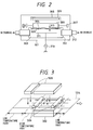
- Fig. 1 is a diagrammatic cross-sectional view to illustrate an example of the constitution of a film forming apparatus.
- Fig. 2 is a diagrammatic cross-sectional view to illustrate a state in which the web is transported within the film forming space.
- Figs. 3 to 5 are each a diagrammatic perspective view to illustrate how the web deforms.
- Figs. 6 and 9 are each a diagrammatic cross-sectional view to illustrate a state in which the web is transported according to the present invention.
- Figs. 7 and 10 are each a diagrammatic perspective view to illustrate how the web is deformed in the present invention.
- Fig. 8 is a diagrammatic cross-sectional view to illustrate a preferred example of the constitution of a film forming apparatus.
- Fig. 11 is a diagrammatic cross-sectional view to illustrate an example of a film forming chamber.
- Fig. 12 is a diagrammatic perspective view to illustrate an example of a steering mechanism.
- deposited films are formed while bringing into a specific shape as the transverse sectional shape of the web that forms a part of a discharge space. More specifically, the above objects can be achieved by a deposited-film forming process comprising continuously transporting a web in a length direction of the web so as to form a part of a discharge space, and continuously forming a deposited film on the web, wherein the web is transported while bringing its transverse sectional shape into a curved shape.
- the curved shape may have either an upward convex curve or a downward convex curve, and the curve may be an oval curve or a curve having two or more points of inflection.
- the web may be kept plane at a region other than the region where the web is transported while bringing its transverse sectional shape into the curved shape. Also, the web may be transported along the curved surface formed at the open area of the discharge space on its web transport side.
- the deposited films may of course be formed by plasma-assisted CVD, and also the process of the present invention enables formation of semiconductor layers having achieved the above objects.
- a deposited-film forming apparatus comprising a web which is lengthwise continuously transported, means for transporting the web so as to form a part of a discharge space, and means for continuously forming a deposited film on the web, wherein the means for transporting the web is provided with a roller for bringing the transverse sectional shape of the web into a curved shape.
- the roller may have the shape of a tsuzumi (a Japanese style hand drum, i.e., a drum with an inward curved body, or a bobbin), or a drum (a drum with an outward curved body, or a barrel), or a gourd with one or more constricted parts.
- the member that constitutes the discharge space has an opening made along the curved shape on the web transport side, and may be provided with a means for keeping the web plane at the part other than the opening made along the curved shape.
- the present invention provides an improvement wherein the transverse sectional shape of the web that forms a part of the discharge space is brought into a curved shape so that the transverse sectional shape of the web may not change every moment during transport because of factors such as heating.
- the shape of the web does not vary in time sequence during transport, and hence no scratches may occur on its film forming surface or on the deposited films formed on the film forming surface to cause no lowering of yield. Further, unstable discharge can be inhibited.
- the radiation heaters (hereinafter “heaters”) are provided right over glow discharge regions (hereinafter “discharge spaces”; not shown) respectively provided in the film forming chambers 1101, 1102, 1103, 1104, 1105 and 1106.
- the heaters heat the web 1107 to the desired temperature.
- the back of the film forming surface of the web 1107 is heated by the heaters when the web 1107 has been transported right over the discharge spaces. Meanwhile, the film forming surface is exposed to plasma, and heated with plasma to have a high temperature.
- the present inventors have found that the shape of the web heated on the discharge space may change in the form of waves, having several peaks, like webs 304 and 504 as shown in Figs. 2 and 3. They also found that the shape of this deformation changes with time.
- RF power In the continuous plasma-assisted CVD apparatus 1100 of a roll-to-roll system as shown in Fig. 1, either RF power or microwave power can be used. This example will be described on an instance where the microwave power is used.
- reference numeral 301 denotes a film forming chamber; 302, a discharge box; 303, a discharge space; 304, a web; 305, an opening adjuster plate; 306, a cylindrical magnet roller; 307, a bearing; 308, a heater; 309, a reflector; 310, an RF oscillator; 311, an antenna; 312, an applicator; and 313, a clearance.
- Fig. 2 is a schematic cross section as viewed on the web transport side.
- a discharge box 302 with a size of 200(D) ⁇ 140(H) ⁇ 400(W) mm is internally provided.
- the opening adjuster plate 305 is provided in the discharge box 302 on its side facing the web 304 at the web inlet side and the web outlet side each.
- the size of the opening adjuster plate may be changed, whereby the time for which the web is exposed to plasma can be changed to thereby obtain a film deposited on the web in a desired thickness.
- the discharge space 303 has a nozzle or hole (not shown) through which film forming gases are fed into the discharge space.
- SiH 4 gas, GeH 4 gas and H 2 gas are respectively fed into the discharge space at gas flow rates of SiH 4 120 SCCM, GeH 4 120 SCCM and H 2 200 SCCM.
- the inside of the discharge space has a pressure of, i.e., 12.0 mmTorr.
- microwave power with a frequency of 2.45 GHz and an output of 400 W were applied through the applicator 321 to generate plasma in the discharge space.
- High-frequency waves with a frequency of 13.56 MHz and an output of 1,500 W were further applied from the RF oscillator 310 to the antenna 311 for applying RF bias power.
- the web was heated by the lamp heater 308 (500 W ⁇ 10 lamps in total) provided right over the discharge box so as to have a web temperature of 300°C.
- the distance (clearance) 313 between the opening adjuster plate 305 and the magnet roller 306 was set to be, for example, 4 mm.
- the magnet roller 306 used had a cylindrical form.
- amorphous silicon compound films were continuously formed on the web over a period of 5 hours.
- the shape of the web changed to wave shape in the width direction of the web when it stood right over the discharge box 302 or 502, as shown in Fig. 2 or 3.
- the wave of deformation was in a period of 180 mm in the width direction.
- the deformation was limited by it to have a degree of deformation of 4 mm as amplitude.
- the web at its deformation peaks came in contact with the opening adjuster plate 305 to cause deep cut scratches on the film forming surface and to break semiconductor junctions, causing a problem of what is called a shunt. This causes a great decrease in yield.
- the clearance of the web path at the discharge box was broadened to 10 mm to make the same experiments as the above.
- the scratches caused by the contact of the web with the opening adjuster plate less occurred, plasma leaked outside from the discharge space through the clearance to cause a problem of unstable microwave discharge.
- the continuous plasma-assisted CVD apparatus for continuously forming films on the web including the apparatus of a roll-to-roll system
- the back of the film forming surface of the web is heated by the heaters and the film forming surface is heated with plasma to have a high temperature.
- the temperature of the web drops chiefly because of radiant cooling.
- the web is repeatedly heated and cooled in this way at every time it is passed through a plurality of discharge spaces.
- the high temperature part of the web has a large web width than the low temperature part because of thermal expansion.
- the expansion in the thickness direction is very small and is considered to be substantially negligible.
- the expansion in the transport direction is small as compared with the long transport path, and is substantially negligible because of the expansion in the transport direction.
- Figs. 3 and 4 schematically illustrate instances where the web 404 or 504 continuously has the high temperature part and the low temperature part. Magnet rollers that support the web are illustrated as instances where cylindrical magnet rollers are used.
- the thin sheet When compressive force or tensile force acts on a thin sheet, the thin sheet tends to strain in the direction perpendicular to the direction of the force, as known in general. Hence, the web deforms in the direction perpendicular to the web surface because of the compressive force.
- the web is made of SUS430 and has a width of 360 mm and a thickness of 0.125 mm at room temperature, 25°C.
- Fig. 5 diagrammatically illustrates a cross section of the web.
- the web has a width l of 360 mm.
- the transport direction is represented by x, and the width direction falling at right angles with it, by y.
- the shape of the web which is flat at 25°C is shown by broken lines.
- the strain quantity Q reaches as much as 17 mm at, e.g., web temperature of 300°C, and hence the clearance on the discharge space inlet side and outlet side through which the web is passed can not be made smaller than that.
- the heated web has a transverse sectional shape which is neither arc nor plane, and spontaneously deforms in waves as shown in Fig. 2.
- the web comes into linear contact with the magnet rollers, and hence a strong magnetic attraction force is obtained.
- the web also constitutes a part of the discharge space, and hence, in order to stably maintain microwave plasma discharge, it is preferred that the shape and size of the discharge space constituted of the discharge box and the web and the gap between the discharge space and the outside thereof are always constant. Since, however, the shape of the web is not constant in time sequence, this variation in shape damages the stability of discharge.
- the heater controls temperature by controlling its output, in order to keep the web at a predetermined temperature. Since, however, the web has a small heat capacity, even a small variation in heater output causes variation in web temperature. Hence, the expansion of the web changes to cause a change in the form due to strain. Namely, there is a high possibility that the shape of the web is not constant in time sequence in view of the flow-in and flow-out of the heat.
- the shape of the web is not constant in time sequence.
- the continuous plasma-assisted CVD apparatus is incorporated with a steering mechanism as will be described later, as a mechanism for putting a wind-up roll end in order.
- the tension in the width direction has a difference in magnitude between the case when the steering mechanism stands driven and the case when it stands stopped. This difference affects the shape of the web.
- the shape of the web is not constant in time sequence.
- the strained form of the web changes in variety with changes in web temperature, with repetition of drive and stop of the steering mechanism and with transport of the web.
- the shape of the web varies in time sequence, it is difficult to make the opening adjuster plate not come in contact with the web, and even when the gap is provided between them, the film forming surface is scratched to cause a decrease in yield and unstable discharge.
- the transverse sectional shape of the web constituting a part of the discharge space is brought into a curved shape so that the web is fitted to the peripheral shape of the magnet roller according to the present invention, to thereby making the web free of any changes occurring every moment in its transverse sectional shape.
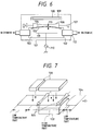
- Fig. 6 cross-sectionally illustrates the apparatus according to the present invention. Its cross section falls at right angles with the web transport direction.
- reference numeral 101 denotes a film forming chamber; 102, a discharge box; 103, a discharge space; 104, a web; 105, an opening adjuster plate; 106, a hand drum (or bobbin) type magnet roller; 107, a bearing; 108, a heater; 109, a reflector; 110, an RF oscillator; 111, an antenna; 112, an applicator; and 113, a clearance.
- the roller 106 has a cross-sectional shape concavely curved toward the middle as its cross section along the shaft.
- the film forming chamber 101 is one of three semiconductor thin-film forming chambers of a roll-to-roll type plasma-assisted CVD apparatus shown in Fig. 8, which will be detailed later, and is picked up as an example that can be preferably used in an i-type layer forming chamber 854.
- the film forming chamber 101 has a vacuum retaining means, a gas feed-discharge means, a power supply means, a web heating means and a web transport means.
- the discharge space 103 is defined by inner walls of the discharge box 102 and the surface of the web 104.
- desired materials gases are fed, and desired microwave power is supplied through the applicator to thereby cause glow discharge to take place and decompose the material gases.
- an RF power outputted from the RF oscillator 110 is applied to the plasma through the antenna to form desired semiconductor films on the web 104.
- the web 104 is previously heated to a desired temperature by means of the heater 108.
- the web 104 has a transverse sectional shape having an upward convex, oval curve.
- the bobbin type magnet roller 106 has also a cross section having an upward convex, oval curve (i.e., an inversely corresponding concave line) at its part coming in contact with the web 104.
- the opening adjuster plate 105 has a top end also having the same shape as the oval curve so that the web 104 serving as a top cover can be transported while keeping an upward convex, curved surface.
- the discharge box 102 has substantially the shape of a rectangular solid, and its top is constituted of the opening and the opening adjuster plate.
- the two sides facing the transport direction each have the shape of a figure formed of three straight lines and one curve corresponding to the top end of the opening adjuster plate 105.
- the other two sides facing each other in the direction perpendicular to the former sides (i.e. the width direction) and the bottom each have the shape of a rectangular.
- the bobbin type magnet roller 106 is provided one by one in the vicinity of the inlet and the outlet each, of the discharge box 102.
- the web 104 magnetically attracted with this bobbin type magnet roller 106 is forcedly deformed by the bobbin type magnet roller 106 without regard to the web temperature to have the upward convex, curved surface.
- the web 104 is brought into contact with the bobbin type magnet roller 106 along its periphery without regard to the web temperature, and hence the force of magnetic attraction can well acts.
- the shape of the web 104 is changed in similar figures along the oval curve when the web 104 undergo thermal expansion as a result of heating, and is elongated by a size corresponding to thermal expansion coefficient.
- the web 104 comes to have not the shape spontaneously deformed in waves as shown in Fig. 3 but the upward convex, curved surface as shown in Fig. 7.
- the web 104 is heated neither by the plasma nor by the heater when it stands transported to the part outside the discharge box 102, and is radiantly cooled there, so that the temperature of the web 104 drops.
- the shape of the web 104 returns to the original plane and hence the shape of the web 104 is returned to a plane by natural cooling or forced cooling before it enters into the gas gate.
- the magnet roller is not limited to the bobbin type magnet roller 106 as described above, which brings the transverse sectional shape of the web 104 into the upward convex, overly curved line as shown in Fig. 6.
- the same effect as in the case of Fig. 6 can be obtained also using a drum (or barrel) type magnet roller 206 which deforms the web in a downward convex, oval curve as shown in Fig. 9, or a gourd type magnet roller which deforms the web in a curve having two or more points of inflection as shown in Fig. 10.
- Fig. 9 is a diagrammatic cross-sectional view of an apparatus preferably usable as, e.g., a first doped layer forming chamber 802 or a second doped layer forming chamber 803 of a roll-to-roll system type plasma-assisted CVD apparatus 800 as shown in Fig. 8. While in the apparatus shown in Fig. 6 the plasma is generated using microwaves, the apparatus shown in Fig. 9 is so made up that plasma is generated using RF power.
- reference numeral 201 denotes a film forming chamber; 202, a discharge box; 203, a discharge space; 204, a web; 205, an opening adjuster plate; 206, a drum (or barrel) type magnet roller; 210, an RF oscillator; 211, a discharge electrode; and 213, a clearance.
- the roller 206 has a cross-sectional shape convexly curved toward the middle as its cross section along the shaft.
- the apparatus shown in Fig. 9 is operated in substantially the same manner as that shown in Fig. 6, except that an RF voltage is applied between the discharge electrode 211 and the web 204 to thereby cause glow discharge to take place and decompose the material gases fed into the discharge space 203.
- apparatus constitution is shown in which the barrel type magnet roller 206 is used as a magnet roller.
- the web 204 magnetically attracted with this barrel type magnet roller 206 is deformed to have the downward convex, curved surface, which is inverse to that of the apparatus shown in Fig. 6.
- the shape of the web 204 is changed in similar figures along the downward convex, oval curve when the web 104 undergo thermal expansion as a result of heating.
- the web When a gourd type magnet roller as shown in Fig. 10 is used, the web can be forcedly deformed into a shape similar to the shape of spontaneous deformation of the web, i.e., the shape approximate to the wavy form of the web 504 shown in Fig. 3. Since the web is kept to have the shape approximate to the spontaneous deformation, the shape of the web can be stabler. In this instance, although the web is deformed in waves, the problems as previously discussed can be prevented because such a shape is under control. Moreover, the same effect can be obtained by the magnet roller having the diameter of the widest part smaller than that of the widest part of the bobbin type or barrel type magnet roller, so that the apparatus can be made smaller in size.
- the shape of the roller by which the web is deformed is by no means limited to those described above, and may be appropriately modified.
- the web transport and film formation can be made stable by making the shape of the web stable.
- the shape of the roller of the i-type layer forming chamber and the shape of the roller of the doped layer forming chamber are also by no means limited to those described above.
- the use of the process and apparatus constituted according to the present invention makes it possible for the web to keep a constant shape as it stands along the periphery of the magnet roller when the web is heated and transported, and hence enables apparatus constitution having the following three features.
- the present invention will be further described below by giving Examples, chiefly in respect of the sequential relationship of the film forming chamber 101, including the disposition of gas gates and the steering mechanism, and the plasma-assisted CVD apparatus of a roll-to-roll system.
- Fig. 8 is a diagrammatic cross-sectional view to illustrate an example of the plasma-assisted CVD apparatus 800 of a roll-to-roll system according to the present invention.
- an i-type semiconductor layer is simply called an i-type layer, and a doped semiconductor layer as a doped layer.
- reference numeral 801 denotes a substrate wind-off chamber; 802, a first doped layer forming chamber; 803, a second doped layer forming chamber; 804, a substrate wind-up chamber; 805 to 809, temperature control mechanisms such as heaters; 810 to 813, gas gates; 814 to 820, vacuum gauges; 821 to 827, gas feed pipes; 828 to 832, gas exhaust duct; 833, a wind-off bobbin; 834, a web; 835, a wind-up bobbin; 836 to 848, magnet rollers; 849 and 850, high-frequency oscillator; 851, 852' and 853, discharge spaces; 852, an i-type layer forming chamber; and 854, a microwave inlet.
- temperature control mechanisms such as heaters; 810 to 813, gas gates; 814 to 820, vacuum gauges; 821 to 827, gas feed pipes; 828 to 832, gas exhaust duct; 833, a wind-off bobbin; 834
- the plasma-assisted CVD apparatus 800 of a roll-to-roll system as shown in Fig. 8 is constituted chiefly of film forming chambers, material gas feed means, gas separating means, exhaust means, transport means, power supply means, and substrate temperature control means.
- This plasma-assisted CVD apparatus 800 of a roll-to-roll system can form semiconductor layers for single-cell of, e.g., pin-type photovoltaic devices.
- a power with a frequency of 13.56 MHz or 100 kHz is usually used.
- the high-frequency power sources 849 and 850 are by no means limited to those having the above frequency, and any of those of 50 kHz to 10 GHz may be used. It, however, necessary to appropriately control film forming conditions when those with frequencies other than the foregoing are used. Especially when frequencies of 50 MHz or above are selected, pressure may preferably be set at 5 to 20 mTorr.
- the microwaves led into the discharge space 852 in which the i-layer is formed may also be any of low-ripple types continuously oscillating at frequencies of microwave bands.
- microwaves need not necessarily be used so long as a discharge space length large enough to well ensure the thickness of the i-layer can be taken.
- the web gate is a mechanism similar to a gate valve having a square opening, used to vacuum-sealing the web by up and down interposing it with elastomers.
- the wave gate is useful when the web is exchanged or the film forming chambers are put to maintenance care.
- the wave gate is effective for preventing time efficiency of the apparatus from lowering because of opening to the atmosphere, when the apparatus has a number of film forming chambers and their maintenance care must be taken at different timing.
- This wave gate may have such a size that it structurally has an opening wider than the width of the web and allows the belt-like substrate to pass with ease.
- the wave gate enables vacuum sealing at a low leakage, using conventional fluorine rubber as the elastomer so long as the web has a thickness smaller than 0.3 mm.
- the elastomer is not limited to fluorine rubber. It, however, must fulfill the conditions that it has an elasticity and a low leakage, it does not break at the web end and it does not cause an increase in leakage even when the web gate is repeatedly opened and closed.
- the wave gate may preferably be provided in pair at the positions adjacent to the gas gates 810 and 813 shown in Fig. 8, and also be provided in pair at the positions adjacent to the gas gates 811 and 812. That is, the former gates are provided in order to exchange web rolls, and the latter gates to take maintenance care of the inside of the i-type layer forming chamber.
- films are formed at a low rate in the first doped layer forming chamber and second doped layer forming chamber and at a high rate in the i-type layer forming chamber, and hence the maintenance care of the i-type layer forming chamber is more frequently taken so that the time efficiency of the apparatus 800 as a whole can be improved.
- one end of the web 834 is fixed to the wind-up bobbin 835, and the web is transported by driving the wind-up bobbin 835 through means provided outside the wind-up bobbin chamber 804.
- the tension of the web 834 is produced by causing a force reverse to the transport direction to act on the wind-off bobbin 833.
- the force may be caused to act through a clutch provided outside the wind-off bobbin chamber 801.
- a powder clutch is preferred.
- Fig. 11 is a diagrammatic cross-sectional view to illustrate an example of the inside of the first and second doped layer forming chambers 802 and 803 each as shown in Fig. 8.
- reference numeral 900 denotes a doped layer forming chamber; 901, a high-frequency electrode; 902, a web; 903, a gas feed pipe; 904, a gas heater; 905, a lamp heater; 906, a gas blow outlet; 907, a exhaust duct; 908, a magnet roller; 909, a gas gate; 910, a gate gas feed pipe; 911, web transport direction; 912, a discharge space; 913, a separation passageway; 914, a thermocouple; 915, gate rollers; and 916, a gate gas exhaust duct.
- the high-frequency power source 849 having a frequency of 13.56 MHz or 100 kHz is electrically connected as described with reference to Fig. 8, and the high-frequency power is supplied thereto.
- this frequency may be changed as occasion calls.
- the material gases are passed through the gas feed pipe 903 and flowed beneath the gas heater 904 toward the right as viewed in the drawing. Next, the material gases are flowed over the gas heater toward the left as viewed in the drawing, and are preheated.
- the material gases are blowed out through the gas blow outlet 906, and are flowed inside the film forming chamber 912 toward the right as viewed in the drawing, the chamber being surrounded by the high-frequency electrode 901 and the web 902. Then the gases are flowed downward from the right end of the discharge space 912 and exhausted outside the doped layer forming chamber 900 by means of a vacuum pump through the exhaust duct 907.
- the web 834 is passed through the gas gates 810 to 813, and magnetically attracted by the magnet rollers 836 to 848 so as to be hung down.
- the web is passed through the gas gate 909 in such a state that it is passed through the discharge space 912 and is again hung down with the magnet roller 908. Then, the web is transported through the transport path as shown in Fig. 8.
- the magnet rollers 836 to 848 employ the bobbin type magnet roller according to the present invention.
- the web 104 cooled to room temperature by the gas gate (not shown) is transported into the film forming chamber in the state that its transverse sectional shape is substantially flat.
- the web is heated to a desired temperature. Because of its thermal expansion at this time, the web spontaneously deforms into irregular waves whose transverse sectional shape varies every moment, to cause scratches on the film forming surface and a decrease in yield and also make discharge stability poor.
- the barrel type magnet roller 106 is provided on the inlet side and outlet side of the discharge space 102 so that the transverse sectional shape of the web 104 is forcedly curved to form an upward convex, oval curve to thereby maintain a constant shape free of any changes occurring every moment.
- the discharge box 102 is upward convexly curved in its external shape of the top, and its top opening is made to have an upward convex, curved surface so as to be fit along the curved web 104.
- the gap between the web and the discharge box opening can be made narrower, whereby the plasma can be enclosed at a high proportion to bring about an improvement in discharge stability.
- the web is also more elongated on the film forming surface side than the film forming back side, and hence the thin film formed thereon tends to be compressed when, e.g., the web 104 is cooled to room temperature to return to substantially a flat state after film formation has been completed through the discharge space.
- the convexly curved, barrel type roller used when the web 104 has a smaller expansion coefficient than the thin film, can make smaller the stress applied to the thin film, and can be expected to bring about an advantage that the film separation less occurs.
- the concavely curved, bobbin type roller used when the web has reversely a larger expansion coefficient than the thin film, can be expected to bring about a similar advantage.
- the web 104 having come out of the discharge space 102 is naturally cooled by heat dissipation or forcedly cooled by a cooling roller additionally provided, so that the transverse sectional shape of the web 104 returns to substantially a plane, and the web is further transported in that state.
- the position and number of the bobbin type magnet roller 106 are not limited to what has been described above, and may be appropriately adjusted according to uses.
- the gas gate has both the function of gas separation and the function as a passageway for the web.
- the function of gas separation can be achieved in the following way: Adjoining film forming chambers are connected through a slit-shaped separation passageway, and a separating gas (gate gas) is flowed in the separation passageway so as to strike against the material gases, to thereby shorten the diffusion length of the material gases.
- a separating gas gate gas
- the web 902 is passed through a separation passageway 913 of the gas gate 909.
- the web is transported in the state that the top surface of the web 902 is brought into close contact with gate rollers 915 each having a plurality of grooves internally provided with a permanent magnet and the back surface of the web 902 serving as the film forming surface is in non-contact.
- the gate gas is fed through the gate gas feed pipe 910 into the separation passageway 913 so as to be flowed toward the upper and the lower surfaces of the web.
- the flow rate of the gate gas may preferably be designed taking account of the pressure difference of film forming chambers adjacent to the feed pipe, the inner size of the gas gate, the mutual diffusion coefficient of the separating gas and material gas, the tolerance of mutual diffusion, the maximum quantity of gas exhaust and so forth.
- the gate gas fed through the gate gas feed pipe 910 is passed through the separation passageway 913 and flowed into the film forming chambers adjoining to its both sides.
- the gate gas flowed into the doped layer forming chamber is flowed into the gas gate exhaust duct 916 provided beneath the discharge space 912 so that it can be prevented from mixing into the discharge space 912.
- the inner size of the gas gate 909 i.e., the size of the separation passageway 913 may preferably be as narrow as possible in the thickness direction of the web and as long as possible in the transport direction.
- the size of the separation passageway may preferably be as wide as possible in the thickness direction of the web and as short as possible in the transport direction.
- the size of the separation passageway may preferably be set within the range of usually from about 0.3 mm to about 5 mm in the thickness direction of the web, from about 200 mm to about 700 mm in the transport direction and about 20 mm plus web width in the width direction, which must be further taken account of the thickness and transport speed of the web.
- the film forming chamber 854 having the lowest pressure for forming the i-layer therein requires a severe tolerance of mutual diffusion from the doped layer forming chamber, and hence the size of the separation passageway is set within the range of from about 0.3 mm to about 3 mm in the thickness direction and from about 300 mm to about 700 mm in the transport direction.
- the size of the separation passageway is set within the range of from about 1 mm to about 5 mm in the thickness direction and from about 200 mm to about 500 mm in the transport direction.
- the web temperature decreases by radiation from the top surface of the web 902 and the web temperature increases by heat coming from plasma.
- the quantity of radiant heat form the web depends on the surface properties of the web and the residence time of the web in the discharge space 912.
- the quantity of heat coming from plasma depends on the film forming conditions and the residence time of the web in the discharge space 912.
- the temperature of the web 902 changes in variety while it is passed through the discharge space 912. Accordingly, the web temperature may be appropriately controlled by sparsely arranging lamps with nearer approach to the outlet of the discharge space 912 or by additionally providing a cooling means.
- the substrate wind-up chamber 804 may preferably be provided therein with a lateral shift detecting mechanism and a steering mechanism for correcting the lateral shift.
- Fig. 12 is a sketch showing examples of the lateral shift detecting mechanism and steering mechanism.
- the web 834 is partly broken to make illustration.
- Fig. 12 shows an instance where the web is deformed in waves.
- reference numeral 1001 denotes the lateral shift detecting mechanism; 1002, a rotating mechanism; 1003, a roller; 1004, web transport direction; 1005, a bearing; and 1006, a transport speed detecting encoder.
- the web 834 is upward curved at the roller 1003 to change its transport direction 1004.
- the roller 1003 is set rotatable within horizontal plane by means of the rotating mechanism 1002 via the bearing 1005.
- the steering mechanism has the roller 1003, the bearing 1005 and a rotating mechanism 1002.
- This rotating mechanism 1002 is connected to a motor (not shown) via a speed reducer (not shown) so that the rotational angle can be controlled from the outside of the substrate wind-up chamber 804.
- the wind-up bobbin 835, the rotating shaft 1002 and the bearing 1005 are positionally adjusted in advance so that the same tension is applied to the right and left of the roller 1003 and the web 834 is wound up on the wind-up bobbin 835 in order.
- the amount of lateral shift of the lateral shift detecting mechanism is regarded as 0, and the rotational angle ⁇ of the rotating shaft 1002, as 0°.
- the rotating mechanism 1002 is also rotated in such a way that the left side of the roller 1003 moves toward the back side and the right side of the roller 1003 towards the front side with respect to the transport direction 1004, i.e., moves clockwise.
- the lateral shift detecting mechanism 1001 is provided at least at one end of the web 834 in its width direction.
- the lateral shift detecting mechanism 1001 may preferably be provided inside the substrate wind-up chamber 804 and set as close as possible to the roller 103.
- the roller 1003 and the lateral shift detecting mechanism are provided at a distance inevitably, any lowering of sensitivity and delay of response caused by such distance may be compensated by software.
- the mechanism constituted in this way makes it possible to achieve a high-speed response when the web is transported at a wide transport speed range of from 0.2 to 5 m/min. as measured by means of the transport speed detecting encoder 1006, and to wind up the web in order.
- Step 1 to Step 11 An example of a process for producing a photovoltaic device by using the plasma-assisted CVD 800 of a roll-to-roll system of the present invention, shown in Fig. 8, will be described below in the order of steps shown below as Step 1 to Step 11.
- Step 1 is the step of setting a web having been cleaned in a predetermined manner.
- the web wound around the wind-off bobbin 833 is set to a predetermined position. While winding off the web from the wind-off bobbin 833, the gas gate 810, first doped layer forming chamber 802, gas gate 811, i-type layer forming chamber 854, gas gate 812, second doped layer forming chamber 803 and gas gate 813 are all opened at the respective top covers thereof, and the web is passed through these in this order. Then, the leading end of the web is fixed to the wind-up bobbin 835 to make ready so that the web can be wound up on the wind-up bobbin 835.
- the magnet rollers 836 to 848 are checked to make sure that all of them come into contact with the non-film-forming surface of the web.
- Step 2 is the step of transporting the web in the atmosphere, making sure of the transport and stopping the transport.
- web driving means such as a wind-up bobbin rotating mechanism (not shown) and a supporting transport roller driving mechanism (not shown) are checked to make sure that the web is continuously transported without difficulties by that means in the atmosphere.
- the web driving means may preferably have both the function of forward movement and the function of backward movement, and also may preferably have an indicator of web wind-off quantity.
- the web is returned to the initial setting position while monitoring the web wind-off quantity indicator, and is stopped at that position.
- Step 3 is the step of evacuating the insides of the film forming chambers having therein the web and transport means.
- the respective film forming chambers having therein the web and transport means are closed at their top covers, and the insides of the respective film forming chambers are evacuated by means of vacuum pumps.
- the i-type layer forming chamber 854 its inside is roughly evacuated to nearly 10 -3 Torr by means of a rotary pump and a mechanical booster pump, and thereafter fully evacuated by means of an oil diffusion pump. Taking this procedure, its inside is continuously evacuated until the pressure inside the discharge box reaches 6 ⁇ 10 -6 Torr.
- Step 4 is the step of feeding material gases into the discharge box.
- gases are led to a mixing panel (not shown) from gas cylinders (not shown) through a stainless steel pipe (not shown), the mixing panel being a means by which gases are mixed and gas flow rates are precisely controlled.
- the material gases controlled at predetermined flow rates by a mass flow controller (not shown) provided in the mixing panel are fed into the discharge boxes 851 to 853 through the gas feed pipes 821 to 823.
- the evacuation capacity of the vacuum pumps and the exhaust conductance of the exhaust pipes are previously selected so that the internal pressure of the discharge boxes 851 to 853 each is kept at a predetermined value.
- Step 5 is the step of controlling temperature of the web.
- the web is controlled to a predetermined temperature by means of a temperature control means (not shown) while flowing material gases.
- microwave plasma-assisted CVD apparatus since microwave plasma-assisted CVD apparatus has a higher electron density and a higher electron temperature than RF plasma-assisted CVD apparatus, the web temperature tends to rise because of heat coming from plasma.
- Equilibrium temperature of the web depends on the microwave power to be applied in the state that the temperature control mechanism is not operated.
- the equilibrium temperature under conditions as shown in Table 2 is as shown in Table 3.
- Table 2 Web material SUS 430 BA (bright annealed) Film forming chamber size: 13.4 (D) ⁇ 14 (H) ⁇ 40 (W) cm Film forming conditions: Material gas flow rate: SiH 4 , 99 sccm Pressure: (10 ⁇ 1) ⁇ 10 -3 Torr Bias voltage: RF 1,500 W Bias current: about 3.0
- Microwave power 140 W ⁇ 2 Web equilibrium temperature: 270°C
- the above temperature control mechanism is operated to control the temperature to the desired value.
- the web temperature can be controlled to a predetermined value by similarly measuring the equilibrium temperature and optimizing the performance of the temperature control mechanism.
- Step 6 is the step of discharging high frequency (film forming step 1).
- high-frequency waves are oscillated from an RF power source or microwave power source to apply an RF power or microwave power into the discharge boxes 851 to 853 through coaxial cables or waveguides.
- the material gases fed inside the discharge boxes 851 to 853 are ionized with the electric power.
- uniform deposited films are formed on the web at its portions corresponding to the insides of the discharge boxes 851 to 853.
- the power is controlled by a tuner so that reflected power is not more than 20% of incident power in the ionized state.
- An RF voltage is applied to bias electrodes (not shown).
- Step 7 is the step of transporting the web (film forming step 2).
- the web is transported in order to continuously form the deposited films on the web, after the plasma emission produced by the discharging in the above Step 6 and the bias currents have become stable.
- Step 8 is the step of cooling the web and stopping its transport.
- the web transport, high-frequency discharge and temperature control are stopped after the deposited films are continuously formed while transporting the web as previously described and the web wound around the wind-off bobbin has almost run short.
- the web wind-off length detector previously described or a detector of wind-off bobbin external diameter may be used as means for detecting the residue of the web wound around the wind-off bobbin.
- the web In order to take out the web on which the deposited films have been formed, to put them in the atmosphere, the web must be cooled in advance.
- the web may preferably be gradually cooled, and the material gases are kept flowed for a while after the high-frequency discharging is stopped.
- Step 9 is the step of stopping feed of the material gases.
- the material gases are flowed for about 5 minutes and thereafter the feeding of the material gases are stopped.
- an inert gas He gas
- He gas is flowed at a flow rate of about 200 sccm.
- the feeding of the inert gas is stopped, and thereafter the remaining gas is exhausted. Then, the discharge boxes 851 to 853 are evacuated until their internal pressure reaches 2 ⁇ 10 -5 Torr.
- Step 10 is the step of leaking nitrogen in the film forming chambers.
- this Step 10 in order to return the internal pressure of the discharge boxes 851 to 853 to atmospheric pressure from 2 ⁇ 10 -5 Torr, dry nitrogen is fed into the discharge boxes.
- a Bourdon tube gauge (not shown) is read to make sure that the pressure of the discharge boxes has returned to atmospheric pressure, the film forming chambers 802 and 803 are opened at the covers thereof, the web on which the deposited films have been formed is taken out of the chambers to put the web in the atmosphere.
- Step 11 is the step of taking out the web.
- the following two ways are generally available to take out the web.
- the above procedure enables stable formation of large-area photovoltaic devices.
- the experiments were made in the following way:
- the plasma-assisted CVD apparatus of a roll-to-roll system as shown in Fig. 8 was continuously operated to produce a-Si (amorphous silicon) cells on a continuous web on which a back reflective layer was already formed.
- transparent electrode films and collector electrodes were formed by vacuum deposition to obtain photovoltaic devices.
- the devices obtained were then irradiated with artificial sunlight to evaluate their photoelectric conversion efficiency.
- the films are formed while transporting the web of 360 m long at a speed of 60 cm/min., and hence the apparatus is driven for 10 hours as continuous operation time.
- the microwave plasma discharge may become extinguished in some cases, and the web transported before the discharge again takes place comes to have faulty portions. This is one factor to cause a decrease in yield.
- the other factor is what is called the shunt, in which scratches or dust occurring on the film forming surface cause a short circuit of cells.
- Characteristics of a-Si cells respectively produced in Test Example and Comparative Example under the common conditions as shown in Table 4 were evaluated by measuring photoelectric conversion efficiency obtained when cells with an area of 0.25 cm 2 were irradiated with artificial sunlight having an AM value of 1.5 and an energy density of 100 mW/cm 2 .
- the photoelectric conversion efficiency is a value obtained by averaging values of efficiency at 20 spots sampled from each web in its full length. Discharge-off times indicate the number of times in which microwave plasma extinguished during 10 hour continuous drive of the apparatus.
- Comparative Example 1 having a large value of clearance, the deposited films had many defective portions because plasma leaked out of the discharge box to frequently cause discharge-off.
- Comparative Example 2 having a small value of clearance, the yield greatly decreased because the web 304 came in contact with the opening adjuster plate 305 to cause the shunt at that portions.
- Test Example almost all the portions were non-defective over the full length of the web.
- the transverse sectional shape of the web transported so as to form a part of the discharge space is brought into a curved shape, whereby the transverse sectional shape of the web can be prevented from varying in time sequence, so that the film forming surface can be made free of scratches to bring about a dramatic improvement in yield.
- the shape of the web which forms a part of the discharge space is kept constant, and hence leakage of discharge can be inhibited and a stable state of discharge can be maintained, whereby deposited films having uniform quality and uniform thickness can be continuously formed.
- roller of the present invention can also be applied in the film forming apparatus as shown in Fig. 1.
Landscapes
- Chemical & Material Sciences (AREA)
- Engineering & Computer Science (AREA)
- General Chemical & Material Sciences (AREA)
- Chemical Kinetics & Catalysis (AREA)
- Materials Engineering (AREA)
- Mechanical Engineering (AREA)
- Metallurgy (AREA)
- Organic Chemistry (AREA)
- Physics & Mathematics (AREA)
- Plasma & Fusion (AREA)
- Chemical Vapour Deposition (AREA)
- Photovoltaic Devices (AREA)
Applications Claiming Priority (3)
| Application Number | Priority Date | Filing Date | Title |
|---|---|---|---|
| JP350359/95 | 1995-12-22 | ||
| JP35035995A JP3332700B2 (ja) | 1995-12-22 | 1995-12-22 | 堆積膜形成方法及び堆積膜形成装置 |
| JP35035995 | 1995-12-22 |
Publications (3)
| Publication Number | Publication Date |
|---|---|
| EP0782176A2 true EP0782176A2 (de) | 1997-07-02 |
| EP0782176A3 EP0782176A3 (de) | 2000-01-12 |
| EP0782176B1 EP0782176B1 (de) | 2008-09-24 |
Family
ID=18409961
Family Applications (1)
| Application Number | Title | Priority Date | Filing Date |
|---|---|---|---|
| EP96120617A Expired - Lifetime EP0782176B1 (de) | 1995-12-22 | 1996-12-20 | Verfahren zum Herstellen abgeschiedener Filme und Vorrichtung zum Herstellen abgeschiedener Filme |
Country Status (6)
| Country | Link |
|---|---|
| US (1) | US6350489B1 (de) |
| EP (1) | EP0782176B1 (de) |
| JP (1) | JP3332700B2 (de) |
| KR (1) | KR100269936B1 (de) |
| CN (1) | CN1124365C (de) |
| DE (1) | DE69637690D1 (de) |
Cited By (11)
| Publication number | Priority date | Publication date | Assignee | Title |
|---|---|---|---|---|
| US6447612B1 (en) | 1999-07-26 | 2002-09-10 | Canon Kabushiki Kaisha | Film-forming apparatus for forming a deposited film on a substrate, and vacuum-processing apparatus and method for vacuum-processing an object |
| EP2102898A4 (de) * | 2006-11-10 | 2011-06-29 | Solopower Inc | Reel-to-reel-reaktion einer vorläuferfolie zur formung einer solarzellenabsorptionsschicht |
| EP2206141A4 (de) * | 2007-10-17 | 2012-10-10 | Yann Roussillon | Anordnung zur verbesserten ablagerung einer lösung |
| US8323735B2 (en) | 2006-10-13 | 2012-12-04 | Solopower, Inc. | Method and apparatus to form solar cell absorber layers with planar surface |
| US8409418B2 (en) | 2009-02-06 | 2013-04-02 | Solopower, Inc. | Enhanced plating chemistries and methods for preparation of group IBIIIAVIA thin film solar cell absorbers |
| EP2336048A4 (de) * | 2008-10-01 | 2013-04-24 | Nippon Electric Glass Co | Glaswalze und verfahren zur bearbeitung der glaswalze |
| US8497006B2 (en) | 2008-10-01 | 2013-07-30 | Nippon Electric Glass Co., Ltd. | Glass roll |
| US8806894B2 (en) | 2008-10-01 | 2014-08-19 | Nippon Electric Glass Co., Ltd. | Process for producing glass roll with a separable protective sheet |
| US9103033B2 (en) | 2006-10-13 | 2015-08-11 | Solopower Systems, Inc. | Reel-to-reel reaction of precursor film to form solar cell absorber |
| US9931816B2 (en) | 2008-10-01 | 2018-04-03 | Nippon Electric Glass Co., Ltd. | Glass roll, device for producing glass roll, and process for producing glass roll |
| EP3327174A1 (de) * | 2016-11-28 | 2018-05-30 | LG Display Co., Ltd. | Walze für walzenherstellungsvorrichtung zur vermeidung von thermischen auswirkungen |
Families Citing this family (32)
| Publication number | Priority date | Publication date | Assignee | Title |
|---|---|---|---|---|
| JP2001288572A (ja) * | 2000-01-31 | 2001-10-19 | Canon Inc | 堆積膜形成装置および堆積膜形成方法 |
| JP4841023B2 (ja) * | 2000-02-10 | 2011-12-21 | 株式会社半導体エネルギー研究所 | 成膜装置及び太陽電池の作製方法 |
| US6667240B2 (en) | 2000-03-09 | 2003-12-23 | Canon Kabushiki Kaisha | Method and apparatus for forming deposited film |
| JP2002020863A (ja) | 2000-05-01 | 2002-01-23 | Canon Inc | 堆積膜の形成方法及び形成装置、及び基板処理方法 |
| US6434514B1 (en) * | 2000-10-13 | 2002-08-13 | Sbc Technology Resources, Inc. | Rule based capacity management system for an inter office facility |
| JP4651072B2 (ja) | 2001-05-31 | 2011-03-16 | キヤノン株式会社 | 堆積膜形成方法、および堆積膜形成装置 |
| JP4560245B2 (ja) * | 2001-06-29 | 2010-10-13 | キヤノン株式会社 | 光起電力素子 |
| JP2004043910A (ja) * | 2002-07-12 | 2004-02-12 | Canon Inc | 堆積膜形成方法および形成装置 |
| US7169323B2 (en) | 2002-11-08 | 2007-01-30 | 3M Innovative Properties Company | Fluorinated surfactants for buffered acid etch solutions |
| JP2006045593A (ja) * | 2004-08-02 | 2006-02-16 | Fuji Electric Holdings Co Ltd | 基板処理装置および基板処理方法 |
| US7666766B2 (en) * | 2005-09-27 | 2010-02-23 | Semiconductor Energy Laboratory Co., Ltd. | Film formation apparatus, method for forming film, and method for manufacturing photoelectric conversion device |
| DE212009000031U1 (de) * | 2008-03-05 | 2010-11-04 | Global Solar Energy, Inc., Tuscon | Vorrichtung zum Aufbringen einer dünnschichtigen Pufferschicht auf einen flexiblen Träger |
| WO2009111052A1 (en) * | 2008-03-05 | 2009-09-11 | Global Solar Energy, Inc. | Heating for buffer layer deposition |
| JP5738601B2 (ja) | 2008-03-05 | 2015-06-24 | ハナジー・ハイ−テク・パワー・(エイチケー)・リミテッド | 薄膜太陽電池セルのための緩衝層蒸着 |
| US20100087015A1 (en) * | 2008-03-05 | 2010-04-08 | Global Solar Energy, Inc. | Feedback for buffer layer deposition |
| US9252318B2 (en) | 2008-03-05 | 2016-02-02 | Hanergy Hi-Tech Power (Hk) Limited | Solution containment during buffer layer deposition |
| DE102008017492B4 (de) * | 2008-04-04 | 2013-07-25 | Von Ardenne Anlagentechnik Gmbh | Verfahren zum Transport eines bandförmigen Substrats und Vakuumbeschichtungsanlage |
| DE102008029379A1 (de) * | 2008-06-23 | 2009-08-13 | Von Ardenne Anlagentechnik Gmbh | Anordnung zum Beschichten bandförmiger Foliensubstrate |
| CN101614620A (zh) * | 2008-06-27 | 2009-12-30 | 深圳富泰宏精密工业有限公司 | 电子装置及其周期性测试方法 |
| JP5238530B2 (ja) * | 2009-01-28 | 2013-07-17 | 富士電機株式会社 | 薄膜製造装置 |
| US20100291308A1 (en) * | 2009-05-14 | 2010-11-18 | Veeco Instruments Inc. | Web Substrate Deposition System |
| US20100310766A1 (en) * | 2009-06-07 | 2010-12-09 | Veeco Compound Semiconductor, Inc. | Roll-to-Roll Chemical Vapor Deposition System |
| US20100310769A1 (en) * | 2009-06-07 | 2010-12-09 | Veeco Compound Semiconductor, Inc. | Continuous Feed Chemical Vapor Deposition System |
| JP5315228B2 (ja) * | 2009-12-25 | 2013-10-16 | 株式会社半導体エネルギー研究所 | 成膜装置及び太陽電池の作製方法 |
| DE102012111484A1 (de) * | 2012-11-27 | 2014-05-28 | Aixtron Se | Vorrichtung und Verfahren zum Bearbeiten streifenförmiger Substrate |
| CN103469163A (zh) * | 2013-09-22 | 2013-12-25 | 无锡启晖光电科技有限公司 | 一种真空镀膜机 |
| JP6375387B2 (ja) * | 2014-04-02 | 2018-08-15 | アプライド マテリアルズ インコーポレイテッドApplied Materials,Incorporated | 真空処理システム、及び処理システムを取り付けるための方法 |
| CN106232867B (zh) * | 2014-04-18 | 2019-01-08 | 株式会社尼康 | 膜形成设备、基板处理设备和装置制造方法 |
| CN108350571A (zh) * | 2015-11-20 | 2018-07-31 | 应用材料公司 | 用于柔性基板的载体 |
| JP6544249B2 (ja) * | 2016-01-19 | 2019-07-17 | 住友金属鉱山株式会社 | キャンロールと真空成膜装置および長尺体の成膜方法 |
| JP6508080B2 (ja) * | 2016-02-05 | 2019-05-08 | 住友金属鉱山株式会社 | キャンロールと長尺体の処理装置および処理方法 |
| JP6721079B2 (ja) * | 2019-04-22 | 2020-07-08 | 住友金属鉱山株式会社 | キャンロールと真空成膜装置および長尺体の成膜方法 |
Citations (3)
| Publication number | Priority date | Publication date | Assignee | Title |
|---|---|---|---|---|
| US4440107A (en) | 1982-07-12 | 1984-04-03 | Energy Conversion Devices, Inc. | Magnetic apparatus for reducing substrate warpage |
| US4485125A (en) | 1982-03-19 | 1984-11-27 | Energy Conversion Devices, Inc. | Method for continuously producing tandem amorphous photovoltaic cells |
| US5510151A (en) | 1989-06-28 | 1996-04-23 | Canon Kabushiki Kaisha | Continuous film-forming process using microwave energy in a moving substrate web functioning as a substrate and plasma generating space |
Family Cites Families (11)
| Publication number | Priority date | Publication date | Assignee | Title |
|---|---|---|---|---|
| GB1542299A (en) * | 1976-03-23 | 1979-03-14 | Warner Lambert Co | Blade shields |
| US4724169A (en) * | 1984-10-09 | 1988-02-09 | Ovonic Synthetic Materials Company, Inc. | Method of producing multilayer coatings on a substrate |
| JPS61159573A (ja) * | 1985-01-07 | 1986-07-19 | Hitachi Ltd | 真空蒸着装置 |
| US4968918A (en) | 1987-07-06 | 1990-11-06 | Kanebo, Ltd. | Apparatus for plasma treatment |
| US4763601A (en) | 1987-09-02 | 1988-08-16 | Nippon Steel Corporation | Continuous composite coating apparatus for coating strip |
| JPH0621358B2 (ja) | 1988-07-15 | 1994-03-23 | 川崎製鉄株式会社 | 長尺基板均一加熱装置 |
| JPH0444335A (ja) | 1990-06-12 | 1992-02-14 | Seiko Epson Corp | 半導体装置の製造方法 |
| JP2714247B2 (ja) * | 1990-10-29 | 1998-02-16 | キヤノン株式会社 | マイクロ波プラズマcvd法による大面積の機能性堆積膜を連続的に形成する方法及び装置 |
| JPH06280026A (ja) * | 1993-03-24 | 1994-10-04 | Semiconductor Energy Lab Co Ltd | 成膜装置及び成膜方法 |
| JP3659512B2 (ja) | 1993-12-20 | 2005-06-15 | キヤノン株式会社 | 光起電力素子及びその形成方法及びその形成装置 |
| JP3571785B2 (ja) | 1993-12-28 | 2004-09-29 | キヤノン株式会社 | 堆積膜形成方法及び堆積膜形成装置 |
-
1995
- 1995-12-22 JP JP35035995A patent/JP3332700B2/ja not_active Expired - Fee Related
-
1996
- 1996-12-18 US US08/768,609 patent/US6350489B1/en not_active Expired - Lifetime
- 1996-12-20 DE DE69637690T patent/DE69637690D1/de not_active Expired - Lifetime
- 1996-12-20 EP EP96120617A patent/EP0782176B1/de not_active Expired - Lifetime
- 1996-12-20 CN CN96123838A patent/CN1124365C/zh not_active Expired - Fee Related
- 1996-12-21 KR KR1019960069916A patent/KR100269936B1/ko not_active Expired - Fee Related
Patent Citations (3)
| Publication number | Priority date | Publication date | Assignee | Title |
|---|---|---|---|---|
| US4485125A (en) | 1982-03-19 | 1984-11-27 | Energy Conversion Devices, Inc. | Method for continuously producing tandem amorphous photovoltaic cells |
| US4440107A (en) | 1982-07-12 | 1984-04-03 | Energy Conversion Devices, Inc. | Magnetic apparatus for reducing substrate warpage |
| US5510151A (en) | 1989-06-28 | 1996-04-23 | Canon Kabushiki Kaisha | Continuous film-forming process using microwave energy in a moving substrate web functioning as a substrate and plasma generating space |
Cited By (14)
| Publication number | Priority date | Publication date | Assignee | Title |
|---|---|---|---|---|
| US6447612B1 (en) | 1999-07-26 | 2002-09-10 | Canon Kabushiki Kaisha | Film-forming apparatus for forming a deposited film on a substrate, and vacuum-processing apparatus and method for vacuum-processing an object |
| US8323735B2 (en) | 2006-10-13 | 2012-12-04 | Solopower, Inc. | Method and apparatus to form solar cell absorber layers with planar surface |
| US9103033B2 (en) | 2006-10-13 | 2015-08-11 | Solopower Systems, Inc. | Reel-to-reel reaction of precursor film to form solar cell absorber |
| EP2102898A4 (de) * | 2006-11-10 | 2011-06-29 | Solopower Inc | Reel-to-reel-reaktion einer vorläuferfolie zur formung einer solarzellenabsorptionsschicht |
| EP2206141A4 (de) * | 2007-10-17 | 2012-10-10 | Yann Roussillon | Anordnung zur verbesserten ablagerung einer lösung |
| US8497006B2 (en) | 2008-10-01 | 2013-07-30 | Nippon Electric Glass Co., Ltd. | Glass roll |
| EP2336048A4 (de) * | 2008-10-01 | 2013-04-24 | Nippon Electric Glass Co | Glaswalze und verfahren zur bearbeitung der glaswalze |
| US8806894B2 (en) | 2008-10-01 | 2014-08-19 | Nippon Electric Glass Co., Ltd. | Process for producing glass roll with a separable protective sheet |
| US9931816B2 (en) | 2008-10-01 | 2018-04-03 | Nippon Electric Glass Co., Ltd. | Glass roll, device for producing glass roll, and process for producing glass roll |
| US10562727B2 (en) | 2008-10-01 | 2020-02-18 | Nippon Electric Glass Co., Ltd. | Glass roll and method of processing glass roll |
| US10781036B2 (en) | 2008-10-01 | 2020-09-22 | Nippon Electric Glass Co., Ltd. | Glass roll with a separable protective sheet |
| US8409418B2 (en) | 2009-02-06 | 2013-04-02 | Solopower, Inc. | Enhanced plating chemistries and methods for preparation of group IBIIIAVIA thin film solar cell absorbers |
| EP3327174A1 (de) * | 2016-11-28 | 2018-05-30 | LG Display Co., Ltd. | Walze für walzenherstellungsvorrichtung zur vermeidung von thermischen auswirkungen |
| US11008656B2 (en) | 2016-11-28 | 2021-05-18 | Lg Display Co., Ltd. | Roll to roll fabrication apparatus for preventing thermal impact |
Also Published As
| Publication number | Publication date |
|---|---|
| EP0782176A3 (de) | 2000-01-12 |
| KR100269936B1 (ko) | 2000-10-16 |
| CN1124365C (zh) | 2003-10-15 |
| JP3332700B2 (ja) | 2002-10-07 |
| DE69637690D1 (de) | 2008-11-06 |
| KR970052053A (ko) | 1997-07-29 |
| US6350489B1 (en) | 2002-02-26 |
| JPH09181005A (ja) | 1997-07-11 |
| EP0782176B1 (de) | 2008-09-24 |
| CN1158912A (zh) | 1997-09-10 |
Similar Documents
| Publication | Publication Date | Title |
|---|---|---|
| US6350489B1 (en) | Deposited-film forming process and deposited-film forming apparatus | |
| US5397395A (en) | Method of continuously forming a large area functional deposited film by microwave PCVD and apparatus for the same | |
| US6338872B1 (en) | Film forming method | |
| EP0406690B1 (de) | Verfahren und Anordnung zur kontinuierlichen Bildung einer durch Mikrowellen-Plasma-CVD niedergeschlagenen grossflächigen Dünnschicht | |
| US5130170A (en) | Microwave pcvd method for continuously forming a large area functional deposited film using a curved moving substrate web with microwave energy with a directivity in one direction perpendicular to the direction of microwave propagation | |
| US6096389A (en) | Method and apparatus for forming a deposited film using a microwave CVD process | |
| US5514217A (en) | Microwave plasma CVD apparatus with a deposition chamber having a circumferential wall comprising a curved moving substrate web and a microwave applicator means having a specific dielectric member on the exterior thereof | |
| US5629054A (en) | Method for continuously forming a functional deposit film of large area by micro-wave plasma CVD method | |
| US5296036A (en) | Apparatus for continuously forming a large area functional deposit film including microwave transmissive member transfer mean | |
| US6855377B2 (en) | Deposited film forming apparatus and deposited film forming method | |
| JPH04247879A (ja) | マイクロ波プラズマcvd法による大面積の機能性堆積膜を連続的に形成する方法及び装置 | |
| JP3659512B2 (ja) | 光起電力素子及びその形成方法及びその形成装置 | |
| US6638359B2 (en) | Deposited film forming apparatus and deposited film forming method | |
| JP3093504B2 (ja) | 光起電力素子及びその形成方法及びその形成装置 | |
| US6526910B2 (en) | Apparatus and method for forming a deposited film by means of plasma CVD | |
| JPH10209479A (ja) | 半導体薄膜及び光起電力素子の作製装置 | |
| US6846521B2 (en) | Apparatus and method for forming deposited film | |
| JP3080515B2 (ja) | ロール・ツー・ロール型マイクロ波プラズマcvd装置 | |
| JP2962840B2 (ja) | マイクロ波プラズマcvd法により大面積の機能性堆積膜を連続的に形成する方法及び装置 | |
| JP3297487B2 (ja) | 光起電力素子及びその形成方法及びその形成装置 | |
| JP2819031B2 (ja) | マイクロ波プラズマcvd法により大面積の機能性堆積膜を連続的に形成する方法及び装置 | |
| JP2819030B2 (ja) | マイクロ波プラズマcvd法により大面積の機能性堆積膜を連続的に形成する方法及び装置 | |
| JPH04187772A (ja) | 堆積膜形成方法及び堆積膜形成装置 | |
| JPH06244118A (ja) | マイクロ波プラズマcvd法により大面積の機能性堆積 膜を連続的に形成する方法及び装置 | |
| JPH09199429A (ja) | 機能性堆積膜の連続的形成装置 |
Legal Events
| Date | Code | Title | Description |
|---|---|---|---|
| PUAI | Public reference made under article 153(3) epc to a published international application that has entered the european phase |
Free format text: ORIGINAL CODE: 0009012 |
|
| AK | Designated contracting states |
Kind code of ref document: A2 Designated state(s): CH DE ES FR IT LI |
|
| PUAL | Search report despatched |
Free format text: ORIGINAL CODE: 0009013 |
|
| AK | Designated contracting states |
Kind code of ref document: A3 Designated state(s): CH DE ES FR IT LI |
|
| 17P | Request for examination filed |
Effective date: 20000605 |
|
| 17Q | First examination report despatched |
Effective date: 20030605 |
|
| 17Q | First examination report despatched |
Effective date: 20030605 |
|
| GRAP | Despatch of communication of intention to grant a patent |
Free format text: ORIGINAL CODE: EPIDOSNIGR1 |
|
| GRAS | Grant fee paid |
Free format text: ORIGINAL CODE: EPIDOSNIGR3 |
|
| GRAA | (expected) grant |
Free format text: ORIGINAL CODE: 0009210 |
|
| AK | Designated contracting states |
Kind code of ref document: B1 Designated state(s): CH DE ES FR IT LI |
|
| REG | Reference to a national code |
Ref country code: CH Ref legal event code: EP |
|
| REF | Corresponds to: |
Ref document number: 69637690 Country of ref document: DE Date of ref document: 20081106 Kind code of ref document: P |
|
| PG25 | Lapsed in a contracting state [announced via postgrant information from national office to epo] |
Ref country code: ES Free format text: LAPSE BECAUSE OF FAILURE TO SUBMIT A TRANSLATION OF THE DESCRIPTION OR TO PAY THE FEE WITHIN THE PRESCRIBED TIME-LIMIT Effective date: 20090104 |
|
| PLBE | No opposition filed within time limit |
Free format text: ORIGINAL CODE: 0009261 |
|
| REG | Reference to a national code |
Ref country code: CH Ref legal event code: PL |
|
| STAA | Information on the status of an ep patent application or granted ep patent |
Free format text: STATUS: NO OPPOSITION FILED WITHIN TIME LIMIT |
|
| PG25 | Lapsed in a contracting state [announced via postgrant information from national office to epo] |
Ref country code: IT Free format text: LAPSE BECAUSE OF FAILURE TO SUBMIT A TRANSLATION OF THE DESCRIPTION OR TO PAY THE FEE WITHIN THE PRESCRIBED TIME-LIMIT Effective date: 20080924 |
|
| 26N | No opposition filed |
Effective date: 20090625 |
|
| REG | Reference to a national code |
Ref country code: FR Ref legal event code: ST Effective date: 20090831 |
|
| PG25 | Lapsed in a contracting state [announced via postgrant information from national office to epo] |
Ref country code: LI Free format text: LAPSE BECAUSE OF NON-PAYMENT OF DUE FEES Effective date: 20081231 Ref country code: CH Free format text: LAPSE BECAUSE OF NON-PAYMENT OF DUE FEES Effective date: 20081231 |
|
| PG25 | Lapsed in a contracting state [announced via postgrant information from national office to epo] |
Ref country code: FR Free format text: LAPSE BECAUSE OF NON-PAYMENT OF DUE FEES Effective date: 20081231 |
|
| PGFP | Annual fee paid to national office [announced via postgrant information from national office to epo] |
Ref country code: DE Payment date: 20131231 Year of fee payment: 18 |
|
| REG | Reference to a national code |
Ref country code: DE Ref legal event code: R119 Ref document number: 69637690 Country of ref document: DE |
|
| PG25 | Lapsed in a contracting state [announced via postgrant information from national office to epo] |
Ref country code: DE Free format text: LAPSE BECAUSE OF NON-PAYMENT OF DUE FEES Effective date: 20150701 |