EP0776075B1 - Laservorrichtung, insbesondere zum optischen Pumpen - Google Patents
Laservorrichtung, insbesondere zum optischen Pumpen Download PDFInfo
- Publication number
- EP0776075B1 EP0776075B1 EP96402465A EP96402465A EP0776075B1 EP 0776075 B1 EP0776075 B1 EP 0776075B1 EP 96402465 A EP96402465 A EP 96402465A EP 96402465 A EP96402465 A EP 96402465A EP 0776075 B1 EP0776075 B1 EP 0776075B1
- Authority
- EP
- European Patent Office
- Prior art keywords
- laser device
- fibre
- active layer
- wafer
- coupling
- Prior art date
- Legal status (The legal status is an assumption and is not a legal conclusion. Google has not performed a legal analysis and makes no representation as to the accuracy of the status listed.)
- Expired - Lifetime
Links
Images
Classifications
-
- H—ELECTRICITY
- H01—ELECTRIC ELEMENTS
- H01S—DEVICES USING THE PROCESS OF LIGHT AMPLIFICATION BY STIMULATED EMISSION OF RADIATION [LASER] TO AMPLIFY OR GENERATE LIGHT; DEVICES USING STIMULATED EMISSION OF ELECTROMAGNETIC RADIATION IN WAVE RANGES OTHER THAN OPTICAL
- H01S5/00—Semiconductor lasers
- H01S5/10—Construction or shape of the optical resonator, e.g. extended or external cavity, coupled cavities, bent-guide, varying width, thickness or composition of the active region
- H01S5/16—Window-type lasers, i.e. with a region of non-absorbing material between the active region and the reflecting surface
-
- H—ELECTRICITY
- H01—ELECTRIC ELEMENTS
- H01S—DEVICES USING THE PROCESS OF LIGHT AMPLIFICATION BY STIMULATED EMISSION OF RADIATION [LASER] TO AMPLIFY OR GENERATE LIGHT; DEVICES USING STIMULATED EMISSION OF ELECTROMAGNETIC RADIATION IN WAVE RANGES OTHER THAN OPTICAL
- H01S5/00—Semiconductor lasers
- H01S5/10—Construction or shape of the optical resonator, e.g. extended or external cavity, coupled cavities, bent-guide, varying width, thickness or composition of the active region
- H01S5/14—External cavity lasers
- H01S5/146—External cavity lasers using a fiber as external cavity
-
- H—ELECTRICITY
- H01—ELECTRIC ELEMENTS
- H01S—DEVICES USING THE PROCESS OF LIGHT AMPLIFICATION BY STIMULATED EMISSION OF RADIATION [LASER] TO AMPLIFY OR GENERATE LIGHT; DEVICES USING STIMULATED EMISSION OF ELECTROMAGNETIC RADIATION IN WAVE RANGES OTHER THAN OPTICAL
- H01S2301/00—Functional characteristics
- H01S2301/18—Semiconductor lasers with special structural design for influencing the near- or far-field
-
- H—ELECTRICITY
- H01—ELECTRIC ELEMENTS
- H01S—DEVICES USING THE PROCESS OF LIGHT AMPLIFICATION BY STIMULATED EMISSION OF RADIATION [LASER] TO AMPLIFY OR GENERATE LIGHT; DEVICES USING STIMULATED EMISSION OF ELECTROMAGNETIC RADIATION IN WAVE RANGES OTHER THAN OPTICAL
- H01S2302/00—Amplification / lasing wavelength
-
- H—ELECTRICITY
- H01—ELECTRIC ELEMENTS
- H01S—DEVICES USING THE PROCESS OF LIGHT AMPLIFICATION BY STIMULATED EMISSION OF RADIATION [LASER] TO AMPLIFY OR GENERATE LIGHT; DEVICES USING STIMULATED EMISSION OF ELECTROMAGNETIC RADIATION IN WAVE RANGES OTHER THAN OPTICAL
- H01S3/00—Lasers, i.e. devices using stimulated emission of electromagnetic radiation in the infrared, visible or ultraviolet wave range
- H01S3/05—Construction or shape of optical resonators; Accommodation of active medium therein; Shape of active medium
- H01S3/06—Construction or shape of active medium
- H01S3/063—Waveguide lasers, i.e. whereby the dimensions of the waveguide are of the order of the light wavelength
- H01S3/067—Fibre lasers
- H01S3/06754—Fibre amplifiers
-
- H—ELECTRICITY
- H01—ELECTRIC ELEMENTS
- H01S—DEVICES USING THE PROCESS OF LIGHT AMPLIFICATION BY STIMULATED EMISSION OF RADIATION [LASER] TO AMPLIFY OR GENERATE LIGHT; DEVICES USING STIMULATED EMISSION OF ELECTROMAGNETIC RADIATION IN WAVE RANGES OTHER THAN OPTICAL
- H01S3/00—Lasers, i.e. devices using stimulated emission of electromagnetic radiation in the infrared, visible or ultraviolet wave range
- H01S3/09—Processes or apparatus for excitation, e.g. pumping
- H01S3/091—Processes or apparatus for excitation, e.g. pumping using optical pumping
- H01S3/094—Processes or apparatus for excitation, e.g. pumping using optical pumping by coherent light
-
- H—ELECTRICITY
- H01—ELECTRIC ELEMENTS
- H01S—DEVICES USING THE PROCESS OF LIGHT AMPLIFICATION BY STIMULATED EMISSION OF RADIATION [LASER] TO AMPLIFY OR GENERATE LIGHT; DEVICES USING STIMULATED EMISSION OF ELECTROMAGNETIC RADIATION IN WAVE RANGES OTHER THAN OPTICAL
- H01S5/00—Semiconductor lasers
- H01S5/02—Structural details or components not essential to laser action
- H01S5/022—Mountings; Housings
- H01S5/0225—Out-coupling of light
- H01S5/02251—Out-coupling of light using optical fibres
-
- H—ELECTRICITY
- H01—ELECTRIC ELEMENTS
- H01S—DEVICES USING THE PROCESS OF LIGHT AMPLIFICATION BY STIMULATED EMISSION OF RADIATION [LASER] TO AMPLIFY OR GENERATE LIGHT; DEVICES USING STIMULATED EMISSION OF ELECTROMAGNETIC RADIATION IN WAVE RANGES OTHER THAN OPTICAL
- H01S5/00—Semiconductor lasers
- H01S5/10—Construction or shape of the optical resonator, e.g. extended or external cavity, coupled cavities, bent-guide, varying width, thickness or composition of the active region
- H01S5/1003—Waveguide having a modified shape along the axis, e.g. branched, curved, tapered, voids
- H01S5/101—Curved waveguide
-
- H—ELECTRICITY
- H01—ELECTRIC ELEMENTS
- H01S—DEVICES USING THE PROCESS OF LIGHT AMPLIFICATION BY STIMULATED EMISSION OF RADIATION [LASER] TO AMPLIFY OR GENERATE LIGHT; DEVICES USING STIMULATED EMISSION OF ELECTROMAGNETIC RADIATION IN WAVE RANGES OTHER THAN OPTICAL
- H01S5/00—Semiconductor lasers
- H01S5/20—Structure or shape of the semiconductor body to guide the optical wave ; Confining structures perpendicular to the optical axis, e.g. index or gain guiding, stripe geometry, broad area lasers, gain tailoring, transverse or lateral reflectors, special cladding structures, MQW barrier reflection layers
- H01S5/22—Structure or shape of the semiconductor body to guide the optical wave ; Confining structures perpendicular to the optical axis, e.g. index or gain guiding, stripe geometry, broad area lasers, gain tailoring, transverse or lateral reflectors, special cladding structures, MQW barrier reflection layers having a ridge or stripe structure
- H01S5/223—Buried stripe structure
Claims (9)
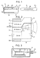
- Laservorrichtung zum optischen Pumpen, welche ein Verstärkersegment (SA) aufweist, das eine aktive Schicht (CA) aufweist, die in einem Halbleiterplättchen (P) ausgebildet ist, wobei das Plättchen (P) von einer ersten und einer zweiten Fläche (F1, F2) begrenzt wird und benachbart zur ersten Fläche (F1) ein Expansionssegment (SE) beinhaltet, um eine Expansion in Transversalrichtung des von der aktiven Schicht (CA) emittierten Lichtes zu ermöglichen, bevor dieses durch die erste Fläche (F1) hindurchgeht, und die aktive Schicht (CA) zwischen einem ersten und einem zweiten Reflektor (BR, F2) angeordnet ist, die einen Resonanzraum bilden, dadurch gekennzeichnet, dass der erste Reflektor (BR) in einer Kopplungsfaser (FC) ausgebildet ist, deren eines Ende (E) sich in der Nähe der ersten Fläche (F1) befindet, wobei die erste Fläche (F1) mit einer Anti-Reflexbeschichtung versehen ist.
- Laservorrichtung nach Anspruch 1, dadurch gekennzeichnet, dass die aktive Schicht (CA) sich über die gesamte Länge des Plättchens (P) erstreckt und sich in derselben Ebene befindet, mit Ausnahme ihres im Expansionssegment (SE) befindlichen Teils.
- Laservorrichtung nach einem der Ansprüche 1 oder 2, dadurch gekennzeichnet, dass das Plättchen (P) aus einem aus Galliumarsenid bestehenden Substrat (1) aufgebaut ist.
- Laservorrichtung nach Anspruch 3, dadurch gekennzeichnet, dass das Expansionssegment (SE) eine Länge (d) zwischen 10 und 50 µm hat.
- Laservorrichtung nach einem der Ansprüche 1 bis 4, dadurch gekennzeichnet, dass das Ende (E) der Kopplungsfaser (FC) in Form eines Diopters endet, dessen Abmessungen derart sind, dass eine maximale optische Kopplung mit dem Plättchen (P) realisiert wird.
- Laservorrichtung nach einem der Ansprüche 1 bis 5, dadurch gekennzeichnet, dass es sich bei der Faser (FC) um eine photosensible Faser handelt und dass der erste Reflektor (BR) ein Bragg-Gitter ist, das am Ende (E) der Kopplungsfaser (FC) durch Photo-Einschreiben erzeugt ist.
- Laservorrichtung nach Anspruch 6, dadurch gekennzeichnet, dass das Bragg-Gitter (BR) eine Länge zwischen 1 und 5 mm hat.
- Laservorrichtung nach einem der Ansprüche 1 bis 7, dadurch gekennzeichnet, dass das Plänchen (P) und das Faserende (E) sich in einem Gehäuse (B) befinden, dessen eine Wand (5) von der Kopplungsfäser (FC) durchstoßen wird und diese in ihrer Position hält.
- Anwendung der Laservorrichtung nach einem der Ansprüche 1 bis 8 zur Durchführung des optischen Pumpens von Erbium-dotierten Fasern.
Applications Claiming Priority (2)
| Application Number | Priority Date | Filing Date | Title |
|---|---|---|---|
| FR9513814 | 1995-11-21 | ||
| FR9513814A FR2741482B1 (fr) | 1995-11-21 | 1995-11-21 | Dispositif laser, notamment pour pompage optique, et son procede de fabrication |
Publications (2)
| Publication Number | Publication Date |
|---|---|
| EP0776075A1 EP0776075A1 (de) | 1997-05-28 |
| EP0776075B1 true EP0776075B1 (de) | 2003-02-12 |
Family
ID=9484779
Family Applications (1)
| Application Number | Title | Priority Date | Filing Date |
|---|---|---|---|
| EP96402465A Expired - Lifetime EP0776075B1 (de) | 1995-11-21 | 1996-11-18 | Laservorrichtung, insbesondere zum optischen Pumpen |
Country Status (6)
| Country | Link |
|---|---|
| US (1) | US5717711A (de) |
| EP (1) | EP0776075B1 (de) |
| JP (1) | JPH09172228A (de) |
| CA (1) | CA2190876C (de) |
| DE (1) | DE69626175T2 (de) |
| FR (1) | FR2741482B1 (de) |
Families Citing this family (12)
| Publication number | Priority date | Publication date | Assignee | Title |
|---|---|---|---|---|
| JPH10221572A (ja) * | 1997-02-07 | 1998-08-21 | Fujitsu Ltd | 光装置 |
| US6327402B1 (en) | 1999-02-04 | 2001-12-04 | Lucent Technologies, Inc. | Lightwave transmission system having wide pump wavebands |
| US6278721B1 (en) | 1999-03-03 | 2001-08-21 | Lucent Technologies, Inc. | Method for minimizing locking range variability of a laser module |
| DE19915569C1 (de) * | 1999-03-30 | 2001-02-01 | Matthias Kuntz | Longitudinal einmodiger, modensprungfrei durchstimmbarer Halbleiterlaser mit Glasfaserkavität und Glasfasergitter |
| FR2793077B1 (fr) * | 1999-04-30 | 2001-07-27 | Cit Alcatel | Laser a gamme de temperature de fonctionnement etendue |
| JP2001185808A (ja) * | 1999-12-22 | 2001-07-06 | Anritsu Corp | 波長可変光源装置 |
| US6625182B1 (en) * | 2000-04-20 | 2003-09-23 | Corning Incorporated | Semiconductor or solid-state laser having an external fiber cavity |
| WO2002103867A1 (de) * | 2001-06-15 | 2002-12-27 | Infineon Technologies Ag | Opto-elektronisches lasermodul |
| US20030064537A1 (en) * | 2001-09-28 | 2003-04-03 | The Furukawa Electric Co., Ltd. | Semiconductor laser device and method for effectively reducing facet reflectivity |
| US7284913B2 (en) * | 2003-07-14 | 2007-10-23 | Matsushita Electric Industrial Co., Ltd. | Integrated fiber attach pad for optical package |
| KR100647904B1 (ko) * | 2004-12-20 | 2006-11-23 | 한국전자통신연구원 | 광섬유 브라그 격자 외부 공진기를 갖는 레이저의제조방법 및 이에 의해 제조된 레이저 |
| KR100713342B1 (ko) * | 2005-05-30 | 2007-05-04 | 삼성전자주식회사 | 광대역 이득 레이저 |
Family Cites Families (13)
| Publication number | Priority date | Publication date | Assignee | Title |
|---|---|---|---|---|
| EP0332723A1 (de) * | 1988-03-15 | 1989-09-20 | International Business Machines Corporation | Hochenergie-Halbleiter-Diodenlaser |
| JPH03195076A (ja) * | 1989-12-25 | 1991-08-26 | Anritsu Corp | 外部共振器型波長可変半導体レーザ |
| US5305335A (en) * | 1989-12-26 | 1994-04-19 | United Technologies Corporation | Single longitudinal mode pumped optical waveguide laser arrangement |
| EP0553994A1 (de) * | 1992-01-29 | 1993-08-04 | AT&T Corp. | Kompakte Quelle für optische Pulse |
| US5337382A (en) * | 1992-05-29 | 1994-08-09 | At&T Bell Laboratories | Article comprising an optical waveguide with in-line refractive index grating |
| US5392308A (en) * | 1993-01-07 | 1995-02-21 | Sdl, Inc. | Semiconductor laser with integral spatial mode filter |
| US5537432A (en) * | 1993-01-07 | 1996-07-16 | Sdl, Inc. | Wavelength-stabilized, high power semiconductor laser |
| US5323404A (en) * | 1993-11-02 | 1994-06-21 | At&T Bell Laboratories | Optical fiber laser or amplifier including high reflectivity gratings |
| US5422897A (en) * | 1994-01-28 | 1995-06-06 | British Telecommunications Public Limited Company | Two-stage mono-mode optical fibre laser |
| FR2720198B1 (fr) * | 1994-05-20 | 1996-07-19 | France Telecom | Laser à fibre optique polarisé linéairement. |
| US5589684A (en) * | 1994-06-28 | 1996-12-31 | Sdl, Inc. | Multiple diode lasers stabilized with a fiber grating |
| US5594747A (en) * | 1995-03-06 | 1997-01-14 | Ball; Gary A. | Dual-wavelength pumped low noise fiber laser |
| US5659644A (en) * | 1996-06-07 | 1997-08-19 | Lucent Technologies Inc. | Fiber light source with multimode fiber coupler |
-
1995
- 1995-11-21 FR FR9513814A patent/FR2741482B1/fr not_active Expired - Fee Related
-
1996
- 1996-11-18 EP EP96402465A patent/EP0776075B1/de not_active Expired - Lifetime
- 1996-11-18 DE DE69626175T patent/DE69626175T2/de not_active Expired - Fee Related
- 1996-11-20 CA CA002190876A patent/CA2190876C/fr not_active Expired - Fee Related
- 1996-11-20 JP JP8309653A patent/JPH09172228A/ja active Pending
- 1996-11-20 US US08/753,093 patent/US5717711A/en not_active Expired - Lifetime
Also Published As
| Publication number | Publication date |
|---|---|
| JPH09172228A (ja) | 1997-06-30 |
| DE69626175T2 (de) | 2003-12-11 |
| FR2741482A1 (fr) | 1997-05-23 |
| US5717711A (en) | 1998-02-10 |
| CA2190876C (fr) | 2000-01-18 |
| CA2190876A1 (fr) | 1997-05-22 |
| FR2741482B1 (fr) | 1997-12-26 |
| EP0776075A1 (de) | 1997-05-28 |
| DE69626175D1 (de) | 2003-03-20 |
Similar Documents
| Publication | Publication Date | Title |
|---|---|---|
| EP0782228B1 (de) | Herstellungsverfahren für einen oberflächenemittierenden Laser | |
| EP0776075B1 (de) | Laservorrichtung, insbesondere zum optischen Pumpen | |
| FR2734097A1 (fr) | Laser a semiconducteurs | |
| FR2522206A1 (fr) | Laser a semi-conducteur | |
| WO2008041138A2 (en) | Coupled cavity ld with tilted wave propagation | |
| FR2743195A1 (fr) | Laser semi-conducteur a emission par la surface | |
| FR2739230A1 (fr) | Composant d'emission laser a cavite verticale a emission par la surface a une longueur d'onde comprise entre 1,3 et 1,5 mu m et procede pour sa realisation | |
| US20080069173A1 (en) | External cavity optoelectronic device | |
| FR2688637A1 (fr) | Laser de puissance a emission par la surface et procede de fabrication de ce laser. | |
| EP0817337B1 (de) | Herstellungsverfahren für einen Oberflächenemittierenden Laser | |
| EP0751594B1 (de) | Festkörpermikrolaser mit aktiver Güteschaltung durch einer Mikromodulator | |
| JPH1056234A (ja) | 改善された半導体レーザおよびそれを製造する方法 | |
| EP0158565B1 (de) | Verfahren zur Herstellung eines Halbleiterlaserspiegels mittels ionischer Bearbeitung | |
| FR2845833A1 (fr) | Amplificateur optique a semiconducteurs a stabilisation de gain laterale et distribuee | |
| FR2770938A1 (fr) | Amplificateur optique semi-conducteur et source laser integree l'incorporant | |
| FR2784811A1 (fr) | Laser a cavite verticale a grande longueur d'onde combine avec un laser de pompage a courte longueur d'onde | |
| EP0399033A1 (de) | Verfahren zur fertigung von halbleiterlasern und mit diesem verfahren hergestellte laser | |
| FR2749447A1 (fr) | Dispositif optique a guide de lumiere semi-conducteur, a faisceau emergent de faible divergence, application aux lasers de fabry-perot et a contre-reaction distribuee | |
| FR3098666A1 (fr) | source de photons uniques à facteur d’indiscernabilité élevé | |
| EP3772145B1 (de) | Hybride laserquelle, die einen integrierten wellenleiter mit einem zwischengeschalteten bragg-gitter umfasst | |
| FR2656432A1 (fr) | Procede de realisation d'un dispositif optoelectronique amplificateur, dispositif obtenu par ce procede et applications a des dispositifs optoelectroniques divers. | |
| EP1433232B1 (de) | Wellenleiterlaserquelle | |
| EP0814544B1 (de) | Halbleiterlaser mit Spiegelbeschichtung und dessen Herstellungsverfahren | |
| KR100931824B1 (ko) | 반도체 양자점 집적광소자 | |
| FR2897726A1 (fr) | Source optique laser a emission verticale |
Legal Events
| Date | Code | Title | Description |
|---|---|---|---|
| PUAI | Public reference made under article 153(3) epc to a published international application that has entered the european phase |
Free format text: ORIGINAL CODE: 0009012 |
|
| AK | Designated contracting states |
Kind code of ref document: A1 Designated state(s): DE ES GB IT NL SE |
|
| 17P | Request for examination filed |
Effective date: 19971001 |
|
| 17Q | First examination report despatched |
Effective date: 20010529 |
|
| RIC1 | Information provided on ipc code assigned before grant |
Free format text: 7H 01S 5/16 A, 7H 01S 3/0941 B |
|
| RTI1 | Title (correction) |
Free format text: LASER DEVICE, IN PARTICULAR FOR OPTICAL PUMPING |
|
| RIC1 | Information provided on ipc code assigned before grant |
Free format text: 7H 01S 5/16 A, 7H 01S 3/0941 B |
|
| RTI1 | Title (correction) |
Free format text: LASER DEVICE, IN PARTICULAR FOR OPTICAL PUMPING |
|
| GRAG | Despatch of communication of intention to grant |
Free format text: ORIGINAL CODE: EPIDOS AGRA |
|
| GRAH | Despatch of communication of intention to grant a patent |
Free format text: ORIGINAL CODE: EPIDOS IGRA |
|
| GRAH | Despatch of communication of intention to grant a patent |
Free format text: ORIGINAL CODE: EPIDOS IGRA |
|
| RAP1 | Party data changed (applicant data changed or rights of an application transferred) |
Owner name: ALCATEL |
|
| GRAA | (expected) grant |
Free format text: ORIGINAL CODE: 0009210 |
|
| AK | Designated contracting states |
Designated state(s): DE ES GB IT NL SE |
|
| PG25 | Lapsed in a contracting state [announced via postgrant information from national office to epo] |
Ref country code: NL Free format text: LAPSE BECAUSE OF FAILURE TO SUBMIT A TRANSLATION OF THE DESCRIPTION OR TO PAY THE FEE WITHIN THE PRESCRIBED TIME-LIMIT Effective date: 20030212 |
|
| REG | Reference to a national code |
Ref country code: GB Ref legal event code: FG4D Free format text: NOT ENGLISH |
|
| GBT | Gb: translation of ep patent filed (gb section 77(6)(a)/1977) |
Effective date: 20030212 |
|
| REF | Corresponds to: |
Ref document number: 69626175 Country of ref document: DE Date of ref document: 20030320 Kind code of ref document: P |
|
| PG25 | Lapsed in a contracting state [announced via postgrant information from national office to epo] |
Ref country code: SE Free format text: LAPSE BECAUSE OF FAILURE TO SUBMIT A TRANSLATION OF THE DESCRIPTION OR TO PAY THE FEE WITHIN THE PRESCRIBED TIME-LIMIT Effective date: 20030512 |
|
| NLV1 | Nl: lapsed or annulled due to failure to fulfill the requirements of art. 29p and 29m of the patents act | ||
| PG25 | Lapsed in a contracting state [announced via postgrant information from national office to epo] |
Ref country code: ES Free format text: LAPSE BECAUSE OF FAILURE TO SUBMIT A TRANSLATION OF THE DESCRIPTION OR TO PAY THE FEE WITHIN THE PRESCRIBED TIME-LIMIT Effective date: 20030828 |
|
| PLBE | No opposition filed within time limit |
Free format text: ORIGINAL CODE: 0009261 |
|
| STAA | Information on the status of an ep patent application or granted ep patent |
Free format text: STATUS: NO OPPOSITION FILED WITHIN TIME LIMIT |
|
| RAP2 | Party data changed (patent owner data changed or rights of a patent transferred) |
Owner name: AVANEX CORPORATION |
|
| 26N | No opposition filed |
Effective date: 20031113 |
|
| PGFP | Annual fee paid to national office [announced via postgrant information from national office to epo] |
Ref country code: DE Payment date: 20081121 Year of fee payment: 13 |
|
| PGFP | Annual fee paid to national office [announced via postgrant information from national office to epo] |
Ref country code: IT Payment date: 20081125 Year of fee payment: 13 |
|
| PGFP | Annual fee paid to national office [announced via postgrant information from national office to epo] |
Ref country code: GB Payment date: 20081117 Year of fee payment: 13 |
|
| GBPC | Gb: european patent ceased through non-payment of renewal fee |
Effective date: 20091118 |
|
| PG25 | Lapsed in a contracting state [announced via postgrant information from national office to epo] |
Ref country code: DE Free format text: LAPSE BECAUSE OF NON-PAYMENT OF DUE FEES Effective date: 20100601 |
|
| PG25 | Lapsed in a contracting state [announced via postgrant information from national office to epo] |
Ref country code: GB Free format text: LAPSE BECAUSE OF NON-PAYMENT OF DUE FEES Effective date: 20091118 |
|
| PG25 | Lapsed in a contracting state [announced via postgrant information from national office to epo] |
Ref country code: IT Free format text: LAPSE BECAUSE OF NON-PAYMENT OF DUE FEES Effective date: 20091118 |