EP0773458B1 - Auflicht-Phasengitter - Google Patents
Auflicht-Phasengitter Download PDFInfo
- Publication number
- EP0773458B1 EP0773458B1 EP95117778A EP95117778A EP0773458B1 EP 0773458 B1 EP0773458 B1 EP 0773458B1 EP 95117778 A EP95117778 A EP 95117778A EP 95117778 A EP95117778 A EP 95117778A EP 0773458 B1 EP0773458 B1 EP 0773458B1
- Authority
- EP
- European Patent Office
- Prior art keywords
- layer
- incident light
- phase grating
- light phase
- grating according
- Prior art date
- Legal status (The legal status is an assumption and is not a legal conclusion. Google has not performed a legal analysis and makes no representation as to the accuracy of the status listed.)
- Expired - Lifetime
Links
- 239000000463 material Substances 0.000 claims abstract description 20
- 238000002310 reflectometry Methods 0.000 claims abstract description 7
- 239000010410 layer Substances 0.000 claims description 104
- 239000000758 substrate Substances 0.000 claims description 11
- VYPSYNLAJGMNEJ-UHFFFAOYSA-N Silicium dioxide Chemical compound O=[Si]=O VYPSYNLAJGMNEJ-UHFFFAOYSA-N 0.000 claims description 4
- 239000011241 protective layer Substances 0.000 claims description 4
- 230000005855 radiation Effects 0.000 claims description 4
- VYZAMTAEIAYCRO-UHFFFAOYSA-N Chromium Chemical compound [Cr] VYZAMTAEIAYCRO-UHFFFAOYSA-N 0.000 claims description 3
- 230000005540 biological transmission Effects 0.000 claims description 3
- 229910000831 Steel Inorganic materials 0.000 claims description 2
- 239000006094 Zerodur Substances 0.000 claims description 2
- 239000010959 steel Substances 0.000 claims description 2
- 229910052681 coesite Inorganic materials 0.000 claims 1
- 229910052906 cristobalite Inorganic materials 0.000 claims 1
- 239000000377 silicon dioxide Substances 0.000 claims 1
- 229910052682 stishovite Inorganic materials 0.000 claims 1
- PBCFLUZVCVVTBY-UHFFFAOYSA-N tantalum pentoxide Inorganic materials O=[Ta](=O)O[Ta](=O)=O PBCFLUZVCVVTBY-UHFFFAOYSA-N 0.000 claims 1
- 229910052905 tridymite Inorganic materials 0.000 claims 1
- 238000000926 separation method Methods 0.000 abstract 1
- 125000006850 spacer group Chemical group 0.000 description 8
- 229910004298 SiO 2 Inorganic materials 0.000 description 4
- 238000004519 manufacturing process Methods 0.000 description 3
- 238000000034 method Methods 0.000 description 3
- NRTOMJZYCJJWKI-UHFFFAOYSA-N Titanium nitride Chemical compound [Ti]#N NRTOMJZYCJJWKI-UHFFFAOYSA-N 0.000 description 2
- PCHJSUWPFVWCPO-UHFFFAOYSA-N gold Chemical compound [Au] PCHJSUWPFVWCPO-UHFFFAOYSA-N 0.000 description 2
- 229910052737 gold Inorganic materials 0.000 description 2
- 239000010931 gold Substances 0.000 description 2
- 238000010327 methods by industry Methods 0.000 description 2
- RYGMFSIKBFXOCR-UHFFFAOYSA-N Copper Chemical compound [Cu] RYGMFSIKBFXOCR-UHFFFAOYSA-N 0.000 description 1
- -1 Invar Chemical compound 0.000 description 1
- 229910001374 Invar Inorganic materials 0.000 description 1
- BQCADISMDOOEFD-UHFFFAOYSA-N Silver Chemical compound [Ag] BQCADISMDOOEFD-UHFFFAOYSA-N 0.000 description 1
- 229910010413 TiO 2 Inorganic materials 0.000 description 1
- 229910052782 aluminium Inorganic materials 0.000 description 1
- XAGFODPZIPBFFR-UHFFFAOYSA-N aluminium Chemical compound [Al] XAGFODPZIPBFFR-UHFFFAOYSA-N 0.000 description 1
- 239000000919 ceramic Substances 0.000 description 1
- 229910052804 chromium Inorganic materials 0.000 description 1
- 239000011651 chromium Substances 0.000 description 1
- 229910052802 copper Inorganic materials 0.000 description 1
- 239000010949 copper Substances 0.000 description 1
- 230000001419 dependent effect Effects 0.000 description 1
- 238000001514 detection method Methods 0.000 description 1
- 238000011161 development Methods 0.000 description 1
- 230000018109 developmental process Effects 0.000 description 1
- 230000000694 effects Effects 0.000 description 1
- 238000005516 engineering process Methods 0.000 description 1
- 239000012535 impurity Substances 0.000 description 1
- 229910052751 metal Inorganic materials 0.000 description 1
- 239000002184 metal Substances 0.000 description 1
- 230000003287 optical effect Effects 0.000 description 1
- 239000005304 optical glass Substances 0.000 description 1
- 230000010363 phase shift Effects 0.000 description 1
- 238000000206 photolithography Methods 0.000 description 1
- 229910052710 silicon Inorganic materials 0.000 description 1
- 239000010703 silicon Substances 0.000 description 1
- 229910052709 silver Inorganic materials 0.000 description 1
- 239000004332 silver Substances 0.000 description 1
Images
Classifications
-
- G—PHYSICS
- G02—OPTICS
- G02B—OPTICAL ELEMENTS, SYSTEMS OR APPARATUS
- G02B5/00—Optical elements other than lenses
- G02B5/18—Diffraction gratings
- G02B5/1861—Reflection gratings characterised by their structure, e.g. step profile, contours of substrate or grooves, pitch variations, materials
-
- G—PHYSICS
- G02—OPTICS
- G02B—OPTICAL ELEMENTS, SYSTEMS OR APPARATUS
- G02B5/00—Optical elements other than lenses
- G02B5/18—Diffraction gratings
- G02B5/1814—Diffraction gratings structurally combined with one or more further optical elements, e.g. lenses, mirrors, prisms or other diffraction gratings
Definitions
- the present invention relates to an incident light phase grating, about that on multiple reflective layers incident light bundle after successful Reflection in a defined way in their relative phase position to each other.
- a reflected light phase grating is particularly suitable for example for use in a photoelectric Position measuring device with which the Relative position of two mutually moving objects is definable.
- phase gratings versus amplitude gratings the advantage of higher diffraction efficiency exhibit. So you can with the help of phase gratings corresponding optical in the beam path Systems have a significantly higher relative proportion of the Intensity of incident partial beams defined bend in certain spatial directions than this possible with comparable amplitude gratings is.
- Usual phase gratings point to the incident partial beams A step grille.
- the stepwise structured surface has disadvantages result if e.g. Impurities in the There are level deepenings and there the Change refractive index undefined. In addition, leaves such a structured surface only with produce increased procedural effort.
- the EP 0 160 784 proposed two spaced, almost planar reflective layers to provide the both sides of a transparent spacer layer are arranged. From the two reflective layers at least one is designed as an amplitude grating.
- the lower of the two reflection layers as continuous Mirror layer, usually as a metal layer educated. Now high in reflection In particular, achieving diffraction efficiencies should the reflectivity of the lower, continuous Mirror layer designed as high as possible his.
- suitable materials for the mirror layer come for example gold, silver, copper or aluminum in question. As a disadvantage at However, these materials prove to be are relatively soft, which in turn is a lack Adhesion of the layers arranged above conditional.
- the object of the present invention is therefore to create a reflected light phase grating that the mentioned Avoids disadvantages of the prior art and in particular enables simple manufacture and ensures high diffraction efficiency.
- the inventive design of an incident light phase grating now guarantees the one desired high reflectance of the lower Layer including a good adhesion of the above arranged layers.
- Second is at the same time ensures that the usually resulting Top layer related problems can be minimized with the structuring. So is not a complex, deep structuring the surface required, rather can almost planar structures are manufactured, which is procedural is significantly less expensive. Therefor can use known mask technologies become.
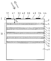
- the incident light phase grating starting from a substrate (1) a specific one Arrangement of the layers provided above specified.
- the substrate material (1) is selected that there is as much stability as possible both mechanical as well as thermal loads having. For example, this is particularly suitable Zerodur, whose coefficient of thermal expansion is almost zero.
- substrate materials come quartz glass, other optical Glasses, steel, such as Invar, and ceramics or Silicon into consideration.
- the stability in terms for possible temperature-related changes in volume or length is especially when using the invention Incident light phase grating in measuring systems for high-precision detection of the relative position two objects of importance.
- Layers (I, II) are provided which are spaced apart are arranged. Both layers (I, II) work at least for part of the incident Reflecting light.
- a spacer layer (2) provided that essentially is transparent to the incident radiation.
- the upper, first layer (I) is designed as an amplitude grating which has periodically alternating regions of different transmission and reflection, hereinafter referred to as bars and gaps.
- the areas of high reflection (3.1, 3.2, 3.3, 3.4) are designed as almost planar, line-shaped areas of a material with high reflectivity.
- a suitable material for this purpose is chromium, for example, which is applied in a thickness of 30-50 nm.
- the typical line width is approximately half of the selected grating period.
- gold or titanium nitride within this layer (I) can also be used as the material of the reflecting regions (3.1, 3.2, 3.3, 3.4).
- the first layer (I) relatively easy using known photolithography methods manufacture or structure.
- Such photolithographic processes for lattice structuring are e.g. from the already cited EP 0 160 784 is well known.
- the second layer (II) is arranged between the spacer layer (2), which will be discussed in more detail later, and the substrate (1), which primarily reflects the transparent areas (4.1, 4.2, 4.3, 4.4) or Gaps in the first layer (I) appearing light beam causes.
- the second layer (II) consists of a dielectric mirror layer, which is composed of several alternating partial layers (5, 6) with a high and low refractive index.
- the refractive indices for the partial layer material with a high refractive index are approximately between 1.8 and 3.0.
- a material is selected for the partial layers (6) with a low refractive index, the refractive index of which is typically in a range between 1.3 and 1.5.
- Suitable materials for the partial layer (5) with a high refractive index are, for example, Ta 2 O 5 or TiO 2 .
- SiO 2 or MgF 2 can be selected for the partial layer (6) with a low refractive index.
- this includes Layer package of the second layer (II) overall five sub-layers (5) with a high refractive index, during four sub-layers (6) with a low refractive index are provided.
- Number of sub-layer pairs for the second layer (II) of the incident light phase grating according to the invention approximately between 4 and 7. From approximately 5 pairs of partial layers provided is a relatively constant reflectivity expected, i.e. also an elevated The number of sub-layer pairs means no significant one Improvement in reflectivity the second layer (II) more.
- a correction factor cos ⁇ i is included in the denominator of the above relationship, where ⁇ i indicates the angle of refraction to the perpendicular in the corresponding layer. Due to the dimensioning instructions explained above, there are of course different layer thicknesses for the partial layers (5, 6) with different refractive indices, ie the partial layers (5) with the high refractive index are thinner than the partial layers (6) with the low refractive index.
- the second layer works (II) an almost complete reflection of the incident Radiation. It also proves advantageous that the dielectric mirror layer (II) is sufficiently hard so that it adheres well the adjacent substrate (I) and with the spacer layer (2) is guaranteed. It results a sufficient mechanical strength of the entire incident light phase grating according to the invention.
- the spacer layer (2) arranged between the two layers (I, II) is also made in the embodiment shown from the material from which the partial layers (6) with the lower refractive index in the second layer (II) are made.
- a suitable choice of the thickness d A of the spacer layer (2) allows the desired resulting phase shift of the partial beams reflected by the different reflection planes to be set in a defined manner.
- the layer thickness is between 0nm and 200nm.
- the top layer of the dielectric layer stack acts as a spacer layer.
- the layer thickness d A is optimized with regard to the respective requirements using suitable numerical methods.
- the first layer (I) is provided with a protective layer and the mechanical strength is thus improved.
- a suitable material for such a protective layer is, for example, SiO 2 , which is applied in a thickness of approximately 100 nm.
- the exemplary embodiment shown in FIG. 1 also has no protective layer.
- Incident light phase grating for example, use in an interferential position measuring device, such as from the EP 0 387 520 is known.
- the reflected light phase grating preferably in a so-called Littrow arrangement for use, as in the Figure indicated by the corresponding arrows should be, i.e. the diffraction angle of the -1. Diffraction order is equal to the angle of incidence of the incident Light.
Landscapes
- Physics & Mathematics (AREA)
- General Physics & Mathematics (AREA)
- Optics & Photonics (AREA)
- Optical Elements Other Than Lenses (AREA)
- Optical Filters (AREA)
- Diffracting Gratings Or Hologram Optical Elements (AREA)
- Holo Graphy (AREA)
Priority Applications (4)
| Application Number | Priority Date | Filing Date | Title |
|---|---|---|---|
| AT95117778T ATE190408T1 (de) | 1995-11-11 | 1995-11-11 | Auflicht-phasengitter |
| DE59507969T DE59507969D1 (de) | 1995-11-11 | 1995-11-11 | Auflicht-Phasengitter |
| EP95117778A EP0773458B1 (de) | 1995-11-11 | 1995-11-11 | Auflicht-Phasengitter |
| JP29416196A JP4073509B2 (ja) | 1995-11-11 | 1996-11-06 | 反射型位相格子 |
Applications Claiming Priority (1)
| Application Number | Priority Date | Filing Date | Title |
|---|---|---|---|
| EP95117778A EP0773458B1 (de) | 1995-11-11 | 1995-11-11 | Auflicht-Phasengitter |
Publications (2)
| Publication Number | Publication Date |
|---|---|
| EP0773458A1 EP0773458A1 (de) | 1997-05-14 |
| EP0773458B1 true EP0773458B1 (de) | 2000-03-08 |
Family
ID=8219805
Family Applications (1)
| Application Number | Title | Priority Date | Filing Date |
|---|---|---|---|
| EP95117778A Expired - Lifetime EP0773458B1 (de) | 1995-11-11 | 1995-11-11 | Auflicht-Phasengitter |
Country Status (4)
| Country | Link |
|---|---|
| EP (1) | EP0773458B1 (enExample) |
| JP (1) | JP4073509B2 (enExample) |
| AT (1) | ATE190408T1 (enExample) |
| DE (1) | DE59507969D1 (enExample) |
Cited By (1)
| Publication number | Priority date | Publication date | Assignee | Title |
|---|---|---|---|---|
| CN101086453B (zh) * | 2006-06-10 | 2011-03-23 | 约翰尼斯海登海恩博士股份有限公司 | 具有反射式相位光栅的标尺 |
Families Citing this family (6)
| Publication number | Priority date | Publication date | Assignee | Title |
|---|---|---|---|---|
| DE10011872A1 (de) * | 2000-03-10 | 2001-09-27 | Heidenhain Gmbh Dr Johannes | Reflexions-Messteilung und Verfahren zur Herstellung derselben |
| DE10150099A1 (de) | 2001-10-11 | 2003-04-17 | Heidenhain Gmbh Dr Johannes | Verfahren zur Herstellung eines Maßstabes, sowie derart hergestellter Maßstab und eine Positionsmesseinrichtung |
| FR2933782B1 (fr) * | 2008-07-11 | 2010-08-13 | Thales Sa | Dispositif de correction des defauts optiques d'un miroir de telescope |
| DE102016201068A1 (de) * | 2016-01-26 | 2017-07-27 | Dr. Johannes Heidenhain Gmbh | Maßverkörperung und Positionsmesseinrichtung mit dieser Maßverkörperung |
| JP7060370B2 (ja) | 2017-12-18 | 2022-04-26 | 株式会社ミツトヨ | スケールおよびその製造方法 |
| DE102019206937A1 (de) * | 2019-05-14 | 2020-11-19 | Dr. Johannes Heidenhain Gmbh | Optische Positionsmesseinrichtung |
Family Cites Families (2)
| Publication number | Priority date | Publication date | Assignee | Title |
|---|---|---|---|---|
| DE3412980A1 (de) * | 1984-04-06 | 1985-10-17 | Dr. Johannes Heidenhain Gmbh, 8225 Traunreut | Auflichtphasengitter und verfahren zur herstellung eines auflichtphasengitters |
| DE3905730C2 (de) * | 1989-02-24 | 1995-06-14 | Heidenhain Gmbh Dr Johannes | Positionsmeßeinrichtung |
-
1995
- 1995-11-11 AT AT95117778T patent/ATE190408T1/de not_active IP Right Cessation
- 1995-11-11 EP EP95117778A patent/EP0773458B1/de not_active Expired - Lifetime
- 1995-11-11 DE DE59507969T patent/DE59507969D1/de not_active Expired - Lifetime
-
1996
- 1996-11-06 JP JP29416196A patent/JP4073509B2/ja not_active Expired - Fee Related
Cited By (1)
| Publication number | Priority date | Publication date | Assignee | Title |
|---|---|---|---|---|
| CN101086453B (zh) * | 2006-06-10 | 2011-03-23 | 约翰尼斯海登海恩博士股份有限公司 | 具有反射式相位光栅的标尺 |
Also Published As
| Publication number | Publication date |
|---|---|
| DE59507969D1 (de) | 2000-04-13 |
| JP4073509B2 (ja) | 2008-04-09 |
| ATE190408T1 (de) | 2000-03-15 |
| JPH09171104A (ja) | 1997-06-30 |
| EP0773458A1 (de) | 1997-05-14 |
Similar Documents
| Publication | Publication Date | Title |
|---|---|---|
| EP0742455B1 (de) | Ma stab und Verfahren zur Herstellung eines Ma stabes sowie Positionsmesseinrichtung | |
| DE3921406C2 (de) | Optische integrierte Schaltung zur Ein- und Auskopplung von Licht | |
| DE3879593T2 (de) | Optische bildumkehrsysteme. | |
| DE10123230A1 (de) | Diffraktives optisches Element sowie optische Anordnung mit einem diffraktiven optischen Element | |
| EP3048426B1 (de) | Positionsmesseinrichtung | |
| EP0212438A2 (de) | Reflexionsbeugungsgitter mit hohem Wirkungsgrad | |
| EP2381280A1 (de) | IR-Neutralfilter mit einem für Infrarotstrahlung transparenten Substrat | |
| DE69317471T2 (de) | Bildlesegerät | |
| EP0773458B1 (de) | Auflicht-Phasengitter | |
| EP0160784B1 (de) | Auflichtphasengitter und Verfahren zur Herstellung eines Auflichtphasengitters | |
| DE10200293B4 (de) | Optische Anordnung sowie Verfahren zur Herstellung einer solchen | |
| EP3150970B1 (de) | Optisches schichtsystem | |
| EP0724168B1 (de) | Positionsmesseinrichtung mit Phasengitter und Herstellungsverfahren | |
| DE3412958A1 (de) | Phasengitter | |
| EP1132719B1 (de) | Reflexions-Messteilung | |
| DE102012101555A1 (de) | Beugungsgitter und Verfahren zu dessen Herstellung | |
| DE10025214C2 (de) | Littrow-Gitter sowie Verwendungen eines Littrow-Gitters | |
| DE3308578C2 (de) | Lichtbrechungskörper zum Konzentrieren von Sonnenstrahlen auf eine Sammelfläche | |
| DE3689438T2 (de) | Phasengitter des zusammengesetzten Muster-Refraktionstyps. | |
| DE3246832A1 (de) | Strahlteiler | |
| DE19639499A1 (de) | Auflicht-Phasengitter | |
| DE10313548B4 (de) | Binär geblazetes diffraktives optisches Element sowie ein solches Element enthaltendes Objektiv | |
| DE102009029324B4 (de) | Reflektives Beugungsgitter | |
| EP0209108A2 (de) | Optisches Element | |
| DE4041047C2 (enExample) |
Legal Events
| Date | Code | Title | Description |
|---|---|---|---|
| PUAI | Public reference made under article 153(3) epc to a published international application that has entered the european phase |
Free format text: ORIGINAL CODE: 0009012 |
|
| 17P | Request for examination filed |
Effective date: 19960502 |
|
| AK | Designated contracting states |
Kind code of ref document: A1 Designated state(s): AT CH DE FR GB IT LI |
|
| GRAG | Despatch of communication of intention to grant |
Free format text: ORIGINAL CODE: EPIDOS AGRA |
|
| GRAG | Despatch of communication of intention to grant |
Free format text: ORIGINAL CODE: EPIDOS AGRA |
|
| GRAH | Despatch of communication of intention to grant a patent |
Free format text: ORIGINAL CODE: EPIDOS IGRA |
|
| 17Q | First examination report despatched |
Effective date: 19990331 |
|
| GRAH | Despatch of communication of intention to grant a patent |
Free format text: ORIGINAL CODE: EPIDOS IGRA |
|
| GRAA | (expected) grant |
Free format text: ORIGINAL CODE: 0009210 |
|
| AK | Designated contracting states |
Kind code of ref document: B1 Designated state(s): AT CH DE FR GB IT LI |
|
| REF | Corresponds to: |
Ref document number: 190408 Country of ref document: AT Date of ref document: 20000315 Kind code of ref document: T |
|
| REG | Reference to a national code |
Ref country code: CH Ref legal event code: NV Representative=s name: TROESCH SCHEIDEGGER WERNER AG Ref country code: CH Ref legal event code: EP |
|
| ET | Fr: translation filed | ||
| REF | Corresponds to: |
Ref document number: 59507969 Country of ref document: DE Date of ref document: 20000413 |
|
| GBT | Gb: translation of ep patent filed (gb section 77(6)(a)/1977) |
Effective date: 20000511 |
|
| PLBE | No opposition filed within time limit |
Free format text: ORIGINAL CODE: 0009261 |
|
| STAA | Information on the status of an ep patent application or granted ep patent |
Free format text: STATUS: NO OPPOSITION FILED WITHIN TIME LIMIT |
|
| 26N | No opposition filed | ||
| REG | Reference to a national code |
Ref country code: GB Ref legal event code: IF02 |
|
| PGFP | Annual fee paid to national office [announced via postgrant information from national office to epo] |
Ref country code: AT Payment date: 20031105 Year of fee payment: 9 |
|
| PG25 | Lapsed in a contracting state [announced via postgrant information from national office to epo] |
Ref country code: AT Free format text: LAPSE BECAUSE OF NON-PAYMENT OF DUE FEES Effective date: 20041111 |
|
| PGFP | Annual fee paid to national office [announced via postgrant information from national office to epo] |
Ref country code: IT Payment date: 20101126 Year of fee payment: 16 |
|
| PGFP | Annual fee paid to national office [announced via postgrant information from national office to epo] |
Ref country code: CH Payment date: 20111123 Year of fee payment: 17 Ref country code: FR Payment date: 20111130 Year of fee payment: 17 |
|
| PGFP | Annual fee paid to national office [announced via postgrant information from national office to epo] |
Ref country code: DE Payment date: 20121121 Year of fee payment: 18 |
|
| PGFP | Annual fee paid to national office [announced via postgrant information from national office to epo] |
Ref country code: GB Payment date: 20121120 Year of fee payment: 18 |
|
| REG | Reference to a national code |
Ref country code: CH Ref legal event code: PL |
|
| PG25 | Lapsed in a contracting state [announced via postgrant information from national office to epo] |
Ref country code: LI Free format text: LAPSE BECAUSE OF NON-PAYMENT OF DUE FEES Effective date: 20121130 Ref country code: CH Free format text: LAPSE BECAUSE OF NON-PAYMENT OF DUE FEES Effective date: 20121130 |
|
| REG | Reference to a national code |
Ref country code: FR Ref legal event code: ST Effective date: 20130731 |
|
| PG25 | Lapsed in a contracting state [announced via postgrant information from national office to epo] |
Ref country code: IT Free format text: LAPSE BECAUSE OF NON-PAYMENT OF DUE FEES Effective date: 20121111 |
|
| PG25 | Lapsed in a contracting state [announced via postgrant information from national office to epo] |
Ref country code: FR Free format text: LAPSE BECAUSE OF NON-PAYMENT OF DUE FEES Effective date: 20121130 |
|
| GBPC | Gb: european patent ceased through non-payment of renewal fee |
Effective date: 20131111 |
|
| PG25 | Lapsed in a contracting state [announced via postgrant information from national office to epo] |
Ref country code: DE Free format text: LAPSE BECAUSE OF NON-PAYMENT OF DUE FEES Effective date: 20140603 |
|
| REG | Reference to a national code |
Ref country code: DE Ref legal event code: R119 Ref document number: 59507969 Country of ref document: DE Effective date: 20140603 |
|
| PG25 | Lapsed in a contracting state [announced via postgrant information from national office to epo] |
Ref country code: GB Free format text: LAPSE BECAUSE OF NON-PAYMENT OF DUE FEES Effective date: 20131111 |