EP0772111A2 - Schaltungsanordnung zur Erzeugung eines Stromes, der proportional zur absoluten Temperatur ist - Google Patents
Schaltungsanordnung zur Erzeugung eines Stromes, der proportional zur absoluten Temperatur ist Download PDFInfo
- Publication number
- EP0772111A2 EP0772111A2 EP96303831A EP96303831A EP0772111A2 EP 0772111 A2 EP0772111 A2 EP 0772111A2 EP 96303831 A EP96303831 A EP 96303831A EP 96303831 A EP96303831 A EP 96303831A EP 0772111 A2 EP0772111 A2 EP 0772111A2
- Authority
- EP
- European Patent Office
- Prior art keywords
- current
- circuit
- transistor
- reference cell
- switch
- Prior art date
- Legal status (The legal status is an assumption and is not a legal conclusion. Google has not performed a legal analysis and makes no representation as to the accuracy of the status listed.)
- Withdrawn
Links
Images


Classifications
-
- G—PHYSICS
- G05—CONTROLLING; REGULATING
- G05F—SYSTEMS FOR REGULATING ELECTRIC OR MAGNETIC VARIABLES
- G05F3/00—Non-retroactive systems for regulating electric variables by using an uncontrolled element, or an uncontrolled combination of elements, such element or such combination having self-regulating properties
- G05F3/02—Regulating voltage or current
- G05F3/08—Regulating voltage or current wherein the variable is DC
- G05F3/10—Regulating voltage or current wherein the variable is DC using uncontrolled devices with non-linear characteristics
- G05F3/16—Regulating voltage or current wherein the variable is DC using uncontrolled devices with non-linear characteristics being semiconductor devices
- G05F3/20—Regulating voltage or current wherein the variable is DC using uncontrolled devices with non-linear characteristics being semiconductor devices using diode- transistor combinations
- G05F3/26—Current mirrors
- G05F3/265—Current mirrors using bipolar transistors only
Definitions
- This invention relates to circuits for generating a current which is proportional to absolute temperature (PTAT), and is particularly concerned with the promotion of a rapid decay of the current when the supply voltage is turned off.
- PTAT proportional to absolute temperature
- the invention is especially concerned with circuits using bipolar devices in which the gain (transconductance) is inversely proportional to absolute temperature, in order that the gain of the bipolar devices may be independent of temperature, by using the PTAT current as bias current.
- an integrated circuit may contain circuits which are switched off frequently, and a rapid turn off of bias currents can be instrumental in prolonging battery life. This could be very important in devices intended to have minimum power consumption, such as radio receiver integrated circuits for paging receivers.
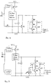
- circuits ( Figure 1) often contain a voltage reference cell, typically a band gap (the energy band gap of a base-emitter junction is used to produce a precise stable reference source of 1.26 volts) and, for reasons of stability and noise decoupling, the voltage reference cell may have a large capacitor (C1) placed across its output. When it is desired to switch the integrated circuit off this large capacitor will cause the voltage reference to decay slowly, along with the bias currents generated from it.
- a pnp switch QP1 ( Figure 2) may be operated from a battery economise control BEC via an interface circuit to switch off I out and other bias currents.
- the current through switch QP1 could be on for a period of one second, but could take as long as one tenth of a second to decay.
- the dotted line shows an enable function controlling the battery economise control BEC.
- the integrated circuit may be required to switch on and off many types a second, with the result that undue current would be taken during the switch off periods.
- the voltage reference cell is shown as a known band gap voltage reference, and the bias current I out is shown being produced by a known peaking current source current reference cell, the outline of which is shown dotted.
- the peaking current source derives its name from the characteristic of I out bias current against I in ( Figure 4), since I out passes through a maximum as I in increases, and I out is relatively insensitive to changes in I in in the region of the peak.
- Such a reference cell is provided in order to provide a well defined output current even if there are small variations of the current through R8 due to its value or the bandgap reference changing.
- the input current I in to the reference cell is defined by R8, and R9 is connected across the bases of matched npn transistors Q8 and Q9. Because of the peaking shape of the characteristic, I out at the peak is proportional to absolute temperature (degrees K) ( Figure 5).
- I out may be typically 10 ⁇ A, firstly, this current is multiplied upwards in the chip, and there might be 2 mA currents related to it and, secondly I out is not proportional to I in in the sense that if I in dropped to half its value I out would perhaps only drop from 10 ⁇ A to 8 ⁇ A.
- the band gap voltage reference thereafter collapses at the original slow rate of 100 ⁇ s referred to in Figure 3.
- the current I out continues to be significant until the potential difference between BEC and VEE has fallen to less than about 0.6 volts. It turns out that the rate of collapse of the band gap voltage reference can still be in the region of 10 to 20 ⁇ s, which is still significant.
- the invention provides a circuit for generating a current which is proportional to absolute temperature, comprising a current source generated from a voltage reference source, a circuit for generating an output current which passes through a maximum as an input current derived from the current source increases and is relatively insensitive to changes in the input current in the region of the maximum, and a path, including a switch, for connecting the current source to ground when the current source is turned off, so as to divert the input current to ground to promote rapid decay in the output current.
- a conductive path is provided for diverting the current source to ground away from the peaking current circuit.
- a transistor Q7 is switched fully on by an interface circuit when BEC goes to a logic level turning band gap voltage reference off, by pulling the base of Q7 towards VCC.
- Q7 is turned hard on and goes into saturation, thereby providing a path for diverting current I in through Q7 to ground, without it passing into the current reference cell to generate I out .
- Q8 and Q9 are turned off hence turning I out off.
- the current through R8 is usually small, compared to the total device current, and the capacitance at node D is only that associated with the parasitics connected to that node. I out can therefore be almost instantaneously turned off, turning off power to the vast majority of the device. This is achieved without having to discharge the capacitor C1.
- Figure 8 shows a possible detailed implementation.
- the circuit is designed such that when the BEC pin is at VCC, the integrated circuit will be on i.e. I out will be generated. When BEC is at VEE, the integrated circuit will be off, i.e. I out will be practically zero.
- X1 is a voltage reference cell that generates a band gap voltage VBG.
- QP1 is a pnp switch to turn X1 off and on, and the circuitry QP5, QP6, Q1, Q2, Q3 and R5 provide the interface between the BEC pin and QP1.
- the resistors R3 and R4 are high value, usually several megohms, to minimise standby current, and are used to set the switching voltage point for the BEC pin. In the example shown, if R3 and R4 have equal values, the voltage switching point of BEC is (VCC - VEE) 2 .
- Transistors QP3, QP4, R1 and R2 provide a very small bias current to provide bias current for the transistors QP5, QP6.
- Transistors Q8, Q9, and resistor R7 form the peaking current source previously described.
- the current I out is replicated many times in the integrated circuit to provide bias currents for various functions in the integrated circuit (not shown).
- C1 is the capacitor, often large in value, used for stability and decoupling of the VBG output voltage.
- Resistor R9, transistors Q10, Q11, QP10 and QP11 provide a small bias current for the transistors QP7 and QP8.
- Transistors QP7, QP8, Q4, Q5, Q6, QP9, R6 and R10 provide the interface for switch Q7.
- transistor QP7 When BEC is set to VEE to disable voltage reference cell X1, transistor QP7 is turned on and transistor QP8 turned off, turning current mirror Q4, Q5 on turning Q6 off.
- the current that flows via resistor R10 now flows into the base of Q7 turning it on, which turns transistors Q8 and Q9 off, and hence I out off.
- Transistor QP9 is provided, with base current limiting resistor R6, such that when BEC is taken to VEE, a larger current than that provided by R10 is used to very rapidly turn Q7 hard on, and hence Q8 and I out off. This enables R10 to be kept at a higher value, and hence reduce its power dissipation when BEC is at VCC.
- R10 is needed to keep Q7 on as QP9 will saturate and the base current supplied via R6 will be reduced, and hence its collector current will be very reduced, when VBG has fallen to around 0.8 to 0.9 volts.
- the integrated circuit may form part of the circuit for the receiver of an R.F. pager, which could operate at between 150-500 MHz carrier frequency and operate at a data rate of between 512 and 2400 bits per second.
- the integrated circuit could provide a data output in 1, 0 format for a microprocessor to interpret the data.
- VCC is 2.7 volts and VEE is ground, but the circuitry described could be used for controlling circuitry run off a lower VCC value of typically 1.3 volts.
- the band gap reference voltage it is possible for the band gap reference voltage to collapse within as little as 1ms from being disabled.
- the voltage reference cell need not be a band gap voltage reference but other types e.g. CMOS voltage reference circuits could be used.
- Other types of peaking current sources could be employed instead of that indicated by transistors Q8, Q9 and resistor R7, and I out need not be used for bias currents.
- FETs could be used in place of the bipolar transistors apart from in the peaking current source.
Landscapes
- Engineering & Computer Science (AREA)
- Microelectronics & Electronic Packaging (AREA)
- Physics & Mathematics (AREA)
- Nonlinear Science (AREA)
- Electromagnetism (AREA)
- General Physics & Mathematics (AREA)
- Radar, Positioning & Navigation (AREA)
- Automation & Control Theory (AREA)
- Control Of Electrical Variables (AREA)
- Amplifiers (AREA)
- Logic Circuits (AREA)
- Electronic Switches (AREA)
Applications Claiming Priority (2)
| Application Number | Priority Date | Filing Date | Title |
|---|---|---|---|
| GB9522274A GB2309606A (en) | 1995-10-31 | 1995-10-31 | Circuits for generating a current which is proportional to absolute temperature |
| GB9522274 | 1995-10-31 |
Publications (2)
| Publication Number | Publication Date |
|---|---|
| EP0772111A2 true EP0772111A2 (de) | 1997-05-07 |
| EP0772111A3 EP0772111A3 (de) | 1998-04-15 |
Family
ID=10783164
Family Applications (1)
| Application Number | Title | Priority Date | Filing Date |
|---|---|---|---|
| EP96303831A Withdrawn EP0772111A3 (de) | 1995-10-31 | 1996-05-29 | Schaltungsanordnung zur Erzeugung eines Stromes, der proportional zur absoluten Temperatur ist |
Country Status (4)
| Country | Link |
|---|---|
| US (1) | US5796294A (de) |
| EP (1) | EP0772111A3 (de) |
| JP (1) | JPH09134223A (de) |
| GB (1) | GB2309606A (de) |
Families Citing this family (4)
| Publication number | Priority date | Publication date | Assignee | Title |
|---|---|---|---|---|
| JP3432425B2 (ja) * | 1998-08-05 | 2003-08-04 | 株式会社東芝 | ゲート回路 |
| US6507238B1 (en) * | 2001-06-22 | 2003-01-14 | International Business Machines Corporation | Temperature-dependent reference generator |
| DE10223996B4 (de) * | 2002-05-29 | 2004-12-02 | Infineon Technologies Ag | Referenzspannungsschaltung und Verfahren zum Erzeugen einer Referenzspannung |
| US7418210B2 (en) * | 2004-03-05 | 2008-08-26 | Finisar Corporation | Programmable transition time adjustment mechanism |
Family Cites Families (10)
| Publication number | Priority date | Publication date | Assignee | Title |
|---|---|---|---|---|
| US4902915A (en) * | 1988-05-25 | 1990-02-20 | Texas Instruments Incorporated | BICMOS TTL input buffer |
| US4999516A (en) * | 1989-07-17 | 1991-03-12 | At&E Corporation | Combined bias supply power shut-off circuit |
| JP3209522B2 (ja) * | 1989-10-18 | 2001-09-17 | テキサス インスツルメンツ インコーポレイテツド | 入力遷移に応答して高速出力遷移を行う出力回路 |
| US4958122A (en) * | 1989-12-18 | 1990-09-18 | Motorola, Inc. | Current source regulator |
| US5481180A (en) * | 1991-09-30 | 1996-01-02 | Sgs-Thomson Microelectronics, Inc. | PTAT current source |
| JP2901434B2 (ja) * | 1992-09-30 | 1999-06-07 | シャープ株式会社 | 直流安定化電源装置 |
| ES2076077B1 (es) * | 1993-05-31 | 1997-08-16 | Alcatel Standard Electrica | Circuito de control de continua en receptores de datos a rafagas. |
| US5448158A (en) * | 1993-12-30 | 1995-09-05 | Sgs-Thomson Microelectronics, Inc. | PTAT current source |
| US5614815A (en) * | 1994-03-10 | 1997-03-25 | Fujitsu Limited | Constant voltage supplying circuit |
| US5459427A (en) * | 1994-05-06 | 1995-10-17 | Motorola, Inc. | DC level shifting circuit for analog circuits |
-
1995
- 1995-10-31 GB GB9522274A patent/GB2309606A/en not_active Withdrawn
-
1996
- 1996-05-29 EP EP96303831A patent/EP0772111A3/de not_active Withdrawn
- 1996-06-13 JP JP8174267A patent/JPH09134223A/ja active Pending
- 1996-06-19 US US08/667,962 patent/US5796294A/en not_active Expired - Fee Related
Also Published As
| Publication number | Publication date |
|---|---|
| GB9522274D0 (en) | 1996-01-03 |
| US5796294A (en) | 1998-08-18 |
| JPH09134223A (ja) | 1997-05-20 |
| EP0772111A3 (de) | 1998-04-15 |
| GB2309606A9 (en) | 1999-11-29 |
| GB2309606A (en) | 1997-07-30 |
Similar Documents
| Publication | Publication Date | Title |
|---|---|---|
| US5084665A (en) | Voltage reference circuit with power supply compensation | |
| US4435678A (en) | Low voltage precision current source | |
| US4788508A (en) | Pop noise suppression circuit for audio amplifier | |
| KR0134914B1 (ko) | 아날로그 방식의 발진회로 | |
| EP0463857B1 (de) | Emittergeerdete Verstärkerschaltung mit Vorspannungsschaltung | |
| US4695750A (en) | Voltage level converting circuit | |
| JP2893429B2 (ja) | 2つの動作モードを有する増幅器 | |
| US4441070A (en) | Voltage regulator circuit with supply voltage ripple rejection to transient spikes | |
| JPH11514193A (ja) | 温度補償増幅器 | |
| US5831473A (en) | Reference voltage generating circuit capable of suppressing spurious voltage | |
| US5796294A (en) | Circuits for generating a current which is proportional to absolute temperature | |
| JPH07152445A (ja) | 電圧発生回路 | |
| US4429270A (en) | Switched current source for sourcing current to and sinking current from an output node | |
| EP0483246B1 (de) | Kombinierte vorspannungsversorgungs- und leistungsunterbrecher-schaltung | |
| US6445166B2 (en) | Power supply circuit in which ripple reducing ability is maintained even when power supply voltage drops | |
| US4525638A (en) | Zener referenced threshold detector with hysteresis | |
| JPH04315207A (ja) | 電源回路 | |
| KR100273830B1 (ko) | 다이오드-바이어스된 차동 증폭기를 갖춘 용량 결합 회로 | |
| US5120998A (en) | Source terminated transmission line driver | |
| US4500831A (en) | Current source | |
| US4614884A (en) | Input interface circuit as a buffer of a logic device to improve the signal to noise ratio of the logic device | |
| US4791325A (en) | Class B clamp circuit | |
| US4918370A (en) | Low voltage-controlled, stand-by electronic circuit with delayed switch off | |
| US5764105A (en) | Push-pull output circuit method | |
| KR100190848B1 (ko) | 오차 전류가 보상된 전류 미러 |
Legal Events
| Date | Code | Title | Description |
|---|---|---|---|
| PUAI | Public reference made under article 153(3) epc to a published international application that has entered the european phase |
Free format text: ORIGINAL CODE: 0009012 |
|
| AK | Designated contracting states |
Kind code of ref document: A2 Designated state(s): AT DE ES FR GB IT |
|
| PUAL | Search report despatched |
Free format text: ORIGINAL CODE: 0009013 |
|
| AK | Designated contracting states |
Kind code of ref document: A3 Designated state(s): AT DE ES FR GB IT |
|
| RAP1 | Party data changed (applicant data changed or rights of an application transferred) |
Owner name: MITEL SEMICONDUCTOR LIMITED |
|
| 17P | Request for examination filed |
Effective date: 19981008 |
|
| 17Q | First examination report despatched |
Effective date: 19981209 |
|
| STAA | Information on the status of an ep patent application or granted ep patent |
Free format text: STATUS: THE APPLICATION IS DEEMED TO BE WITHDRAWN |
|
| 18D | Application deemed to be withdrawn |
Effective date: 19990420 |