EP0772032A2 - In-situ-Temperaturmessung durch Nutzung von Röntgenstrahlenbeugung - Google Patents
In-situ-Temperaturmessung durch Nutzung von Röntgenstrahlenbeugung Download PDFInfo
- Publication number
- EP0772032A2 EP0772032A2 EP96114967A EP96114967A EP0772032A2 EP 0772032 A2 EP0772032 A2 EP 0772032A2 EP 96114967 A EP96114967 A EP 96114967A EP 96114967 A EP96114967 A EP 96114967A EP 0772032 A2 EP0772032 A2 EP 0772032A2
- Authority
- EP
- European Patent Office
- Prior art keywords
- wafer
- ray
- temperature
- further including
- wavelength
- Prior art date
- Legal status (The legal status is an assumption and is not a legal conclusion. Google has not performed a legal analysis and makes no representation as to the accuracy of the status listed.)
- Withdrawn
Links
- 0 C[C@@](C*1)C2*1=C2 Chemical compound C[C@@](C*1)C2*1=C2 0.000 description 1
Images

Classifications
-
- G—PHYSICS
- G01—MEASURING; TESTING
- G01K—MEASURING TEMPERATURE; MEASURING QUANTITY OF HEAT; THERMALLY-SENSITIVE ELEMENTS NOT OTHERWISE PROVIDED FOR
- G01K11/00—Measuring temperature based upon physical or chemical changes not covered by groups G01K3/00, G01K5/00, G01K7/00 or G01K9/00
- G01K11/30—Measuring temperature based upon physical or chemical changes not covered by groups G01K3/00, G01K5/00, G01K7/00 or G01K9/00 using measurement of the effect of a material on X-radiation, gamma radiation or particle radiation
-
- H10P74/00—
-
- G—PHYSICS
- G01—MEASURING; TESTING
- G01N—INVESTIGATING OR ANALYSING MATERIALS BY DETERMINING THEIR CHEMICAL OR PHYSICAL PROPERTIES
- G01N23/00—Investigating or analysing materials by the use of wave or particle radiation, e.g. X-rays or neutrons, not covered by groups G01N3/00 – G01N17/00, G01N21/00 or G01N22/00
- G01N23/20—Investigating or analysing materials by the use of wave or particle radiation, e.g. X-rays or neutrons, not covered by groups G01N3/00 – G01N17/00, G01N21/00 or G01N22/00 by using diffraction of the radiation by the materials, e.g. for investigating crystal structure; by using scattering of the radiation by the materials, e.g. for investigating non-crystalline materials; by using reflection of the radiation by the materials
- G01N23/207—Diffractometry using detectors, e.g. using a probe in a central position and one or more displaceable detectors in circumferential positions
Definitions
- the present invention generally relates to in-situ temperature measurement in semiconductor processing using X-ray diffraction and, more particularly, to in-situ temperature measurement conducted by measuring single crystal substrate (e.g., semiconductor wafer) lattice parameters by X-ray diffraction.
- single crystal substrate e.g., semiconductor wafer
- an in-situ non-contact temperature measurement for single crystal semiconductor substrates like, for example, Si, Ge, or GaAs wafers.
- semiconductor substrates or wafers it is understood that such substrates or wafers may be coated with certain films or structures that usually occur during semiconductor processing.
- Lattice parameters like the so-called lattice constant, are temperature dependent. See, for example, N. W. Ashcroft and N. D. Mermin, Solid State Physics , Saunders, Philadelphia, 1976. Due to precise thermal expansion studies and measurements, the lattice parameters as a function of the temperature are well known for many materials. See, for example, R. S. Krishnan, R. Srinivasan, and S. Devanarayanan, Thermal Expansion of Crystals, Pergamon Press, Oxford, 1979.
- the invention makes it possible to precisely measure the single crystal semiconductor substrate temperature during processing without contacting the semiconductor. More specifically, it allows in-situ process temperature calibration and control.
- This invention applies to all kind of semiconductor processing or manufacturing equipment in which the semiconductor (substrate) temperature is an important process parameter (i.e., thermal processors).
- the invention provides a non-contact in-situ temperature measurement apparatus for a semiconductor wafer, comprising a process chamber housing the semiconductor wafer, an incident X-ray source communicating with the wafer through a communication means in the process chamber, means for receiving reflected x-rays from the wafer, and means for determining the lattice constant of the wafer based on the received reflected X-ray so that the temperature of the wafer may be obtained.
- a method of non-contact in-situ temperature measurement for a semiconductor wafer comprises the steps of providing a single crystal semiconductor (e.g., Si or GaAS) wafer in a process chamber, providing an incident X-ray source communicating with the wafer in the process chamber, receiving reflected X-rays from the wafer, determining the lattice constant of the wafer based on the received reflected X-ray, and obtaining the temperature of the wafer as determined by the lattice constant.
- a single crystal semiconductor e.g., Si or GaAS
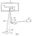
- the X-ray source 12 and diode array detector 14 are located outside the process chamber 16 of a piece of semiconductor processing equipment.
- the incident X-ray beam (bundle of X-rays including, for example, 22a and 23a) and the single reflected X-ray, for example 22b or 23b, respectively, are coupled through one or more windows 18 to the process chamber 16.
- the windows 18 are made of a suitable material such as for example, beryllium.
- the X-ray diffraction can take place either on the backside, on the frontside, or at the edge of the semiconductor wafer 24.
- the X-ray source 12 may be a standard laboratory X-ray source that normally provides a divergent beam containing monochromatic emission lines superimposed on a polychromatic background.
- a monochromator may be used to select radiation of a particular wavelength.
- a bent monochromator 26 with one- or two-dimensional curvature can be used to provide focused monochromatic X-rays.
- the dotted line 30 represents the symmetry axis of the X-ray source/detector unit consisting of source 12 and detector array 14. This axis should be perpendicular to the wafer (backside) surface for a (001) Si wafer, for example.
- the solid line 22b represents a reflected X-ray for some low temperature, say 20°C, while the dotted line 23b represents a reflected X-ray for some high temperature, say 1200°C.
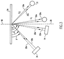
- Figure 2 shows, in more detail, the relationship of the incident and reflected X-rays.
- the angle 2 represents the diffraction angle ⁇ for the incident X-ray 22a and the reflected X-ray 22b
- the angle 3 represents the diffraction angle ⁇ for the incident X-ray 23a and the reflected X-ray 23b. Note that the total scattering angle of the X-ray is 2 ⁇ .
- measurement of the shift ⁇ requires information on the initial wafer temperature T ini in order to determine ⁇ ( a ( T ini )) + ⁇ .
- the X-ray spot 28 on the semiconductor wafer 24 should be very small ( ⁇ 1 ⁇ 2mm, for example) in order to allow precise measurement of the diffraction angle.
- the lattice constant a can be obtained from the Bragg condition.
- the substrate temperature T can be calculated from the thermal expansion relationship by inverting the function a ( T ).
- the position means may include fast mechanical adjustments within the X-ray source/detector unit or software algorithms for correction of measured ⁇ or ⁇ signals.
- Measurement of wafer position or movement can be done, for example, by means of laser light.
- a second diffracted X-ray beam as a reference beam, as shown in Figure 3.
- a first X-ray source and monochromator i.e., X-ray source 12 and monochromator 26 shown in Figure 1 produces incident X-ray beams 22a and 23a at wavelength ⁇ 1 .
- a second reference X-ray source and monochromator 31 produces incident X-ray beams 32a and 33a at wavelength ⁇ 2 , where ⁇ 2 ⁇ 1 .
- the incident beams 32a and 33a produce reflected X-rays 32b or 33b,depending again on the temperature of the wafer 24.
- angle 4 is the diffraction angle ⁇ for a low temperature
- angle 5 is the diffraction angel ⁇ for a high temperature.
- the monochromatic embodiment of the invention will now be considered in greater detail.
- the monochromatic X-ray source 12 is used for the measurement of the lattice constant of (001) silicon substrate wafers.
- the Laue or the equivalent Bragg condition for X-ray diffraction has to be used.
- information on the structure of the semiconductor crystal lattice and the corresponding reciprocal lattice is needed. Reflections or diffraction peaks are denoted by integer indices hkl belonging to corresponding vectors of the reciprocal lattice. Note that vectors of the reciprocal lattice are perpendicular to families of lattice planes in the original crystal lattice.
- the vectors e x , e y , e z are unit vectors along the cubic axes.
- the parameter a is the lattice constant of the face-centered cubic lattice underlying the semiconductor lattice, which is a function of the temperature. At room temperature, a has values 5.43 ⁇ , 5.66 ⁇ , and 5.65 ⁇ for Si, Ge, and GaAs, respectively. See Ashcroft et al., Solid State Physics .
- the reciprocal lattice of the face-centered cubic (fcc) lattice with lattice constant a is body-centered cubic (bcc) with a cubic cell side 4 ⁇ / a .
- n corresponds to the order of the diffraction at the family of ⁇ 004 ⁇ atomic planes in the silicon crystal, if the Bragg picture is used. Those planes have a distance of a /4.
- Equation (7) relates the parameters ⁇ and ⁇ .
- the X-rays are monochromatic and small changes of the Bragg angle ⁇ are measured to provide information on temperature dependent changes of the lattice parameter a .
- Equation (12) the temperature sensitivity in Equation (12) of the Bragg angle ⁇ is larger for higher temperatures because of the increase of ⁇ .
- the sensitivity changes only by a factor of less than 2. The strongest impact on the sensitivity is provided by the reflection angle ⁇ itself because of the increase of tan ⁇ . Back reflection, with ⁇ close to ⁇ /2 is most effective.
- a typical photo diode array detector has around 1024 channels, where individual channels are separated by a distance ⁇ .
- ⁇ denote the distance between wafer and detector
- ⁇ » ⁇ the angular resolution is given by
- the detector should have a small ⁇ and should be placed a great distance ⁇ from the wafer.
- the glancing angle ⁇ should be chosen as close to ⁇ /2 as the construction of the process chamber 16 and the X-ray source 12 and detector array 14 allow.
- the X-ray wavelength ⁇ follows from Equation (7) for a given reflection 001.
- the wavelength ⁇ and the diffraction angle ⁇ must obey the Bragg Equations (6) or (7). This provides an upper limit to the X-ray wavelength: ⁇ ⁇ 2 d 00 l .
- ⁇ should be chosen as close to its upper limit as possible (back reflection).
- silicon one might use one of the following characteristic lines, for example:
- the monochromatic approach according to this invention needs either divergent or convergent incident beams.
- Convergent monochromatic beams can be realized using focussing monochromators (bent crystals).
- sampling times for diode detector arrays with 1024 channels are around l ms.
- the sampling time (inverse of sampling rate) depends on the X-ray beam intensity. Small intensities may result in larger sampling times. For this reason, use of a characteristic X-ray line might be the preferred choice (but this must not hold for characteristic lines of exotic targets in comparison to the Bremsstrahlung intensity of a tungsten target tube, for example). Sampling times from 1 ms up to a 1 second are reasonable.
- the measurement spot was chosen to be located at the backside of a silicon substrate wafer 24 at or near the center.
- the slightly divergent beam coming from the X-ray source 12 was reflected by a bent monochromator crystal 26.
- the choice of monochromator crystal, reflection, and diffraction angles are determined in such a way that the monochromatic beam that reaches the wafer in the small measurement spot 28 has the desired wavelength.
- the use of a bent monochromator crystal 26 allows one to focus the outgoing monochromatic X-rays to the measurement spot 28. Out of the bundle of X-ray beams converging on the measurement spot under different incident angles, only those beams that satisfy the Bragg condition are reflected by the semiconductor wafer 24.
Landscapes
- Chemical & Material Sciences (AREA)
- General Physics & Mathematics (AREA)
- Physics & Mathematics (AREA)
- Biochemistry (AREA)
- Life Sciences & Earth Sciences (AREA)
- Analytical Chemistry (AREA)
- Health & Medical Sciences (AREA)
- General Health & Medical Sciences (AREA)
- Crystallography & Structural Chemistry (AREA)
- Immunology (AREA)
- Pathology (AREA)
- Analysing Materials By The Use Of Radiation (AREA)
- Testing Or Measuring Of Semiconductors Or The Like (AREA)
Applications Claiming Priority (2)
| Application Number | Priority Date | Filing Date | Title |
|---|---|---|---|
| US554209 | 1995-10-24 | ||
| US08/554,209 US5636258A (en) | 1995-10-24 | 1995-10-24 | In-situ temperature measurement using X-ray diffraction |
Publications (2)
| Publication Number | Publication Date |
|---|---|
| EP0772032A2 true EP0772032A2 (de) | 1997-05-07 |
| EP0772032A3 EP0772032A3 (de) | 1998-09-23 |
Family
ID=24212469
Family Applications (1)
| Application Number | Title | Priority Date | Filing Date |
|---|---|---|---|
| EP96114967A Withdrawn EP0772032A3 (de) | 1995-10-24 | 1996-09-18 | In-situ-Temperaturmessung durch Nutzung von Röntgenstrahlenbeugung |
Country Status (5)
| Country | Link |
|---|---|
| US (1) | US5636258A (de) |
| EP (1) | EP0772032A3 (de) |
| JP (2) | JPH09189622A (de) |
| KR (1) | KR970023957A (de) |
| TW (1) | TW310365B (de) |
Cited By (2)
| Publication number | Priority date | Publication date | Assignee | Title |
|---|---|---|---|---|
| RU2240508C1 (ru) * | 2003-03-11 | 2004-11-20 | Малиновский Александр Евгеньевич | Способ коррекции показаний измерительного прибора и устройство для его осуществления (варианты) |
| RU2509298C1 (ru) * | 2012-11-07 | 2014-03-10 | Федеральное государственное бюджетное образовательное учреждение высшего профессионального образования "Национальный исследовательский Томский политехнический университет" | Способ рентгенометрической оценки температурных условий эксплуатации трубных элементов котлов |
Families Citing this family (8)
| Publication number | Priority date | Publication date | Assignee | Title |
|---|---|---|---|---|
| US5978444A (en) * | 1997-12-30 | 1999-11-02 | The United States Of America As Represented By The United States Department Of Energy | Direct detection of x-rays for protein crystallography employing a thick, large area CCD |
| AU2002218653A1 (en) * | 2000-10-13 | 2002-04-29 | Tokyo Electron Limited | Apparatus for measuring temperatures of a wafer using specular reflection spectroscopy |
| US6836532B2 (en) * | 2001-06-29 | 2004-12-28 | Bruker Axs, Inc. | Diffraction system for biological crystal screening |
| EP1571441A1 (de) * | 2004-03-01 | 2005-09-07 | Panalytical B.V. | Überwachung von Epitaxie in situ mittels eines winkeldispersiven Röntgendiffraktometers |
| CN102706474B (zh) * | 2012-06-06 | 2014-01-08 | 常州大学 | 测量物体内部温度的x射线成像设备及其测量的方法 |
| CN108387327B (zh) * | 2018-05-10 | 2024-02-13 | 中国科学院高能物理研究所 | 一种强电离辐射环境下的温度测量方法及系统 |
| CN109374143A (zh) * | 2018-10-30 | 2019-02-22 | 国网江苏省电力有限公司镇江供电分公司 | 干式变压器非接触式内部测温方法 |
| US11609183B2 (en) * | 2020-08-18 | 2023-03-21 | Applied Materials, Inc. | Methods and systems to measure properties of products on a moving blade in electronic device manufacturing machines |
Family Cites Families (16)
| Publication number | Priority date | Publication date | Assignee | Title |
|---|---|---|---|---|
| JPS5744841A (en) * | 1980-09-01 | 1982-03-13 | Hitachi Ltd | Method and apparatus for x-ray diffraction |
| JPS5827031A (ja) * | 1981-08-12 | 1983-02-17 | Agency Of Ind Science & Technol | 温度計測法及び測温素子 |
| NL8300419A (nl) * | 1983-02-04 | 1984-09-03 | Philips Nv | Roentgen analyse apparaat. |
| US4821301A (en) * | 1986-02-28 | 1989-04-11 | Duke University | X-ray reflection method and apparatus for chemical analysis of thin surface layers |
| US5258602A (en) * | 1988-02-17 | 1993-11-02 | Itt Corporation | Technique for precision temperature measurements of a semiconductor layer or wafer, based on its optical properties at selected wavelengths |
| US5167452A (en) * | 1988-02-17 | 1992-12-01 | Itt Corporation | Transmission method to determine and control the temperature of wafers or thin layers with special application to semiconductors |
| US5021980A (en) * | 1989-02-21 | 1991-06-04 | Lsi Logic Corporation | Remote measurement of temperature |
| JPH0318747A (ja) * | 1989-06-16 | 1991-01-28 | Nippon Philips Kk | 格子定数比測定方法及び測定装置 |
| US5208643A (en) * | 1990-10-05 | 1993-05-04 | Varian Associates, Inc. | Method of and apparatus for non-contact temperature measurement |
| US5213985A (en) * | 1991-05-22 | 1993-05-25 | Bell Communications Research, Inc. | Temperature measurement in a processing chamber using in-situ monitoring of photoluminescence |
| US5249865A (en) * | 1992-04-27 | 1993-10-05 | Texas Instruments Incorporated | Interferometric temperature measurement system and method |
| JPH06160309A (ja) * | 1992-11-16 | 1994-06-07 | Mitsubishi Heavy Ind Ltd | 窒化珪素焼結体の表面温度測定方法 |
| JPH06331455A (ja) * | 1993-05-21 | 1994-12-02 | Toshiba Corp | 半導体装置の温度計測方法および温度計測装置ならびに半導体製造装置 |
| JPH0792112A (ja) * | 1993-09-24 | 1995-04-07 | Ricoh Co Ltd | X線評価装置 |
| US5474381A (en) * | 1993-11-30 | 1995-12-12 | Texas Instruments Incorporated | Method for real-time semiconductor wafer temperature measurement based on a surface roughness characteristic of the wafer |
| JP3085070B2 (ja) * | 1993-12-27 | 2000-09-04 | 松下電器産業株式会社 | X線照射装置 |
-
1995
- 1995-10-24 US US08/554,209 patent/US5636258A/en not_active Expired - Fee Related
-
1996
- 1996-09-18 EP EP96114967A patent/EP0772032A3/de not_active Withdrawn
- 1996-10-23 KR KR1019960047604A patent/KR970023957A/ko not_active Ceased
- 1996-10-23 JP JP8281127A patent/JPH09189622A/ja active Pending
- 1996-11-15 TW TW085114011A patent/TW310365B/zh not_active IP Right Cessation
-
2006
- 2006-01-16 JP JP2006007665A patent/JP2006194888A/ja not_active Withdrawn
Cited By (2)
| Publication number | Priority date | Publication date | Assignee | Title |
|---|---|---|---|---|
| RU2240508C1 (ru) * | 2003-03-11 | 2004-11-20 | Малиновский Александр Евгеньевич | Способ коррекции показаний измерительного прибора и устройство для его осуществления (варианты) |
| RU2509298C1 (ru) * | 2012-11-07 | 2014-03-10 | Федеральное государственное бюджетное образовательное учреждение высшего профессионального образования "Национальный исследовательский Томский политехнический университет" | Способ рентгенометрической оценки температурных условий эксплуатации трубных элементов котлов |
Also Published As
| Publication number | Publication date |
|---|---|
| US5636258A (en) | 1997-06-03 |
| KR970023957A (ko) | 1997-05-30 |
| EP0772032A3 (de) | 1998-09-23 |
| TW310365B (de) | 1997-07-11 |
| JP2006194888A (ja) | 2006-07-27 |
| JPH09189622A (ja) | 1997-07-22 |
Similar Documents
| Publication | Publication Date | Title |
|---|---|---|
| US5923720A (en) | Angle dispersive x-ray spectrometer | |
| US10580706B2 (en) | Thin-film fabrication system employing mechanical stress measurement | |
| EP1660874B1 (de) | In-situ-röntgendiffraktionssystem mit quellen und detektoren in positionen mit festem winkel | |
| US6385289B1 (en) | X-ray diffraction apparatus and method for measuring X-ray rocking curves | |
| US6183130B1 (en) | Apparatus for substrate temperature measurement using a reflecting cavity and detector | |
| Angel et al. | High-temperature–high-pressure diffractometry | |
| US5848122A (en) | Apparatus for rapid in-situ X-ray stress measurement during thermal cycling of semiconductor wafers | |
| US5414747A (en) | Method and apparatus for in-process analysis of polycrystalline films and coatings by x-ray diffraction | |
| US5636258A (en) | In-situ temperature measurement using X-ray diffraction | |
| US20030210394A1 (en) | Combination thin-film stress and thickness measurement device | |
| US10620141B2 (en) | Measuring and analyzing residual stresses and their gradients in materials using high resolution grazing incidence X-ray diffraction | |
| EP0635716A1 (de) | Asymmetrischer 4-Kristallmonochromator | |
| US7116754B2 (en) | Diffractometer | |
| JPH05188019A (ja) | X線複合分析装置 | |
| US5164975A (en) | Multiple wavelength X-ray monochromators | |
| US20080075229A1 (en) | Generation of Monochromatic and Collimated X-Ray Beams | |
| EP1617210B1 (de) | Methode und Vorrichtung zum Messen der Reflektivität mittels Röntgenstrahlen | |
| US6174080B1 (en) | Apparatus and methods for measuring substrate temperature | |
| Tao et al. | Non-destructive evaluation of residual stresses in thin films via x-ray diffraction topography methods | |
| Underwood et al. | Beamline for measurement and characterization of multilayer optics for EUV lithography | |
| US8045250B1 (en) | Optical scanning using rotating parallel plate | |
| Tran et al. | Energy calibration for X-ray spectroscopy using powder and single-crystal standards | |
| JP2000213999A (ja) | X線応力測定方法 | |
| Fitch et al. | Analysis of iridium reflectance measurements for AXAF witness mirrors from 2 to 12 keV | |
| SU1744611A1 (ru) | Способ определени радиуса изгиба атомных плоскостей монокристаллических пластин |
Legal Events
| Date | Code | Title | Description |
|---|---|---|---|
| PUAI | Public reference made under article 153(3) epc to a published international application that has entered the european phase |
Free format text: ORIGINAL CODE: 0009012 |
|
| AK | Designated contracting states |
Kind code of ref document: A2 Designated state(s): DE FR GB IT NL |
|
| PUAL | Search report despatched |
Free format text: ORIGINAL CODE: 0009013 |
|
| AK | Designated contracting states |
Kind code of ref document: A3 Designated state(s): DE FR GB IT NL |
|
| 17P | Request for examination filed |
Effective date: 19990323 |
|
| RAP1 | Party data changed (applicant data changed or rights of an application transferred) |
Owner name: KABUSHIKI KAISHA TOSHIBA Owner name: INTERNATIONAL BUSINESS MACHINES CORPORATION Owner name: INFINEON TECHNOLOGIES AG |
|
| RAP1 | Party data changed (applicant data changed or rights of an application transferred) |
Owner name: KABUSHIKI KAISHA TOSHIBA Owner name: INTERNATIONAL BUSINESS MACHINES CORPORATION Owner name: INFINEON TECHNOLOGIES AG |
|
| 17Q | First examination report despatched |
Effective date: 20070807 |
|
| RAP1 | Party data changed (applicant data changed or rights of an application transferred) |
Owner name: KABUSHIKI KAISHA TOSHIBA Owner name: INTERNATIONAL BUSINESS MACHINES CORPORATION Owner name: INFINEON TECHNOLOGIES AG |
|
| STAA | Information on the status of an ep patent application or granted ep patent |
Free format text: STATUS: THE APPLICATION IS DEEMED TO BE WITHDRAWN |
|
| 18D | Application deemed to be withdrawn |
Effective date: 20100401 |