EP0769870B1 - Circuit de synchronisation - Google Patents
Circuit de synchronisation Download PDFInfo
- Publication number
- EP0769870B1 EP0769870B1 EP96460034A EP96460034A EP0769870B1 EP 0769870 B1 EP0769870 B1 EP 0769870B1 EP 96460034 A EP96460034 A EP 96460034A EP 96460034 A EP96460034 A EP 96460034A EP 0769870 B1 EP0769870 B1 EP 0769870B1
- Authority
- EP
- European Patent Office
- Prior art keywords
- circuit
- signal
- synchronization
- horizontal synchronization
- pulses
- Prior art date
- Legal status (The legal status is an assumption and is not a legal conclusion. Google has not performed a legal analysis and makes no representation as to the accuracy of the status listed.)
- Expired - Lifetime
Links
- 230000011664 signaling Effects 0.000 claims description 55
- 238000012937 correction Methods 0.000 claims description 49
- 238000004458 analytical method Methods 0.000 claims description 31
- 238000001514 detection method Methods 0.000 claims description 13
- 230000002035 prolonged effect Effects 0.000 claims 2
- 235000021183 entrée Nutrition 0.000 description 24
- 238000010586 diagram Methods 0.000 description 10
- 101100316752 Arabidopsis thaliana VAL1 gene Proteins 0.000 description 9
- 230000001629 suppression Effects 0.000 description 5
- 238000010200 validation analysis Methods 0.000 description 5
- 101100316753 Arabidopsis thaliana VAL2 gene Proteins 0.000 description 3
- 238000005259 measurement Methods 0.000 description 3
- 230000033764 rhythmic process Effects 0.000 description 3
- 238000000034 method Methods 0.000 description 2
- 238000012545 processing Methods 0.000 description 2
- 238000012800 visualization Methods 0.000 description 2
- 230000004913 activation Effects 0.000 description 1
- 238000012217 deletion Methods 0.000 description 1
- 230000037430 deletion Effects 0.000 description 1
- 238000010894 electron beam technology Methods 0.000 description 1
- 230000000737 periodic effect Effects 0.000 description 1
- 230000000717 retained effect Effects 0.000 description 1
Images


Classifications
-
- H—ELECTRICITY
- H04—ELECTRIC COMMUNICATION TECHNIQUE
- H04N—PICTORIAL COMMUNICATION, e.g. TELEVISION
- H04N5/00—Details of television systems
- H04N5/04—Synchronising
Definitions
- the present invention relates to a circuit for synchronization. It can find its application in the field of monitors, and more particularly in the field of television receivers.
- Such a synchronization circuit allows rhythm the scans of an electron beam on a screen.
- the synchronization signals which it is question contain time information to set the start of a line and the start of a frame.
- a frame is the whole lines needed to form an image on the screen of a monitor.
- Horizontal synchronization signals as well that vertical synchronization signals, called also respectively synchronization signals from line and frame synchronization signals are used to produce, from a loop to phase lock, scan signals necessary to scan the screen with a beam of electrons.
- the signals from synchronization provided to the locking loop of phase are synchronization signals extracted from the video signal.
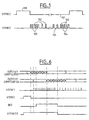
- Figure 1 shows a signal vertical synchronization VSYNCI and a signal HSYNCI horizontal synchronization, both extracted a video signal.
- the synchronization signal vertical VSYNCI is a periodic rectangular signal alternating high level 100, called return pulse frame, and low level 101. During the return pulse frame 100 of the vertical synchronization signal VSYNCI, the functioning of the locking loop phase, which is downstream of the synchronization, is inhibited.
- the synchronization signal HSYNCI is a series of pulses of identically spaced 102 line synchronization in time, each pulse corresponding to the line synchronization.
- This signal has also signaling pulses at the start of frame, 103, and at the end of frame, 104, respectively called post-equalization pulses and pulses pre-equalization.
- the signaling pulses in end of frame, 104 announce the return pulse frame.
- the signaling pulses at the start weft, 103 they are representative of the standard display used.
- the number of lines displayed on the screen varies. While we know currently images with 525 lines and 625 lines, the new standards provide for 1,024 lines. By elsewhere, the refresh rate of the images on the screen, 25 frames per second, also depends standards.
- Phase locked loop comes out then from its operating range.
- a circuit capable of receiving synchronization signals any horizontal and vertical, measure their period or acquire representative information of the shape of these signals, and to produce a signal of horizontal synchronization without pulses signaling 104 at the end of the frame and a signal vertical synchronization including return pulse frame 100 is extended during the pulses of signaling at the start of frame 103.
- the phase locked loop operation is suspended during signaling pulses in start of frame 103 and it no longer receives the signaling pulses at the end of the frame 104.
- An object of the invention is to create a circuit for synchronization can be integrated into all types of monitors.
- FIG. 1a representing a signal of HSYNCI horizontal synchronization and a signal vertical synchronization VSYNCI has been described previously.
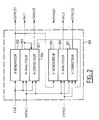
- the synchronization circuit 201 includes a horizontal synchronization generator 202 and a vertical synchronization generator 205 which, in the absence of synchronization in the signals to process by the monitor, provide a signal of horizontal synchronization HSYNCO1 and a signal vertical synchronization VSYNCO1.
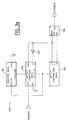
- the synchronization generation circuit horizontal 202 illustrated in FIG. 3a includes a register 8 bit 301, 8 bit counter 302, comparator 8 bits 303, an RS 304 flip-flop and a reverse gate 305.
- the LOAD load input of register 301 is connected to ground.
- OUT ⁇ 7: 0> from the register 301 is connected to the IN ⁇ 7: 0> input of counter 302 and reciprocally.
- the output OUT ⁇ 7: 0> of counter 302 is connected to input IN ⁇ 7: 0> of comparator 303.
- the Rin input of counter 302 is connected to ground.
- the CLK entry of counter 302 receives clock signal CK4MHZ of frequency 4 megahertz and the output Out of the flip-flop RS 304 delivers a horizontal synchronization output signal HSYNCO1.
- the synchronization generation circuit horizontal 202 works as follows: a value representative of the signal period of horizontal synchronization that we are going to produce, is previously stored in register 301. As soon as the counter 302 is loaded with the register value 301, counter 302 starts counting down from this value and at the rate of the clock signal CK4MHZ. When the state of counter 302 is equal to 8, the flip-flop 304 changes state and HSYNCO1 output signal passes to 1. The HSYNCO1 signal returns to 0 when the counter 302 reaches the value 0. Counter 302 is then disabled. It then recharges with the value contained in register 301 and starts again at count down.
- the duration of the high level of the output signal from horizontal synchronization HSYNCO1 is worth 2 microseconds. However, its period is a function of the value contained in register 301.
- the synchronization circuit 201 comprises also a synchronization generation circuit vertical 205 shown in Figure 3b.
- the diagram also includes an RS 310 scale identical to the rocker RS 304.
- the counter 307 counts down to the rhythm of the signal horizontal synchronization HSYNCO1.
- Out of the rocker RS 310 then delivers a signal of vertical synchronization VSYNCO1.
- the signal VSYNCO1 goes to 1 when the state present at output OUT ⁇ 10: 0> of counter 307 is worth 4, and it goes back to 0 when this same state reaches the number 0.
- the synchronization circuit 201 allows also to analyze synchronization signals horizontal as well as synchronization signals vertical present at the entry of the circuit. We can so get information about the shape of these synchronization signals.
- the synchronization circuit 201 includes a synchronization analysis circuit horizontal 203 and an analysis circuit of vertical synchronization 206.
- knowing the number of lines per frame for example can be used by a on-screen message display device for center text in the middle of the screen.
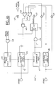
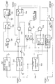
- Figure 4a illustrates a possible embodiment of the horizontal synchronization analysis circuit 203.
- Such a circuit makes it possible to measure the time interval between two line synchronization pulses of a incoming horizontal synchronization signal HSYNCI and to store a value VAL1 representative of this interval in a register. Thereafter, this value VAL1 will be used by the correction circuit of horizontal synchronization 204.
- the circuit 203 is activated during a portion of the synchronization signal horizontal not containing pulses of signage.
- Circuit 203 includes an 8-bit register 401, a 8-bit counter 402, an 8-bit comparator 403 and a rocker RS 406.
- these elements although they are referenced differently, are the same as those used in Figure 3a.
- Register 401, counter 402 and comparator 403 are connected to each other in the same way as the register 301, the counter 302 and the comparator 303 of the circuit 202 illustrated in FIG. 3a.
- the synchronization signal HSYNCI horizontal to analyze attacks the IN input of a falling edge detector 404 and a first input of an OR 410 door.
- the output of the detector 404 is connected to a second input of the AND gate 405 and at a second entrance to the OR gate 411.
- the exit of the door ET 405 is connected to the input of a scale RS 406.
- the RS 406 flip-flop delivers a signal called measurement. This signal goes high after the front descending from a line synchronization pulse HSYNCI signal. Measuring the time interval between two line synchronization pulses occurs when this signal at a high level.
- the Reset input of the flip-flop RS 406 receives an activation signal from circuit 203, MODE_ MEASUREMENT, through a reversing door 413.
- the output Out of this flip-flop is connected by through a 409 reversing door, one second door entrance OR 410.
- the outputs of OR gates, 410 and 411 are each connected to a input of an AND 412 gate, the output of which is connected to the CE validation input for counter 402.
- an AND 414 gate receives on a first input the horizontal synchronization signal to analyze HSYNCI and on a second input the measurement signal delivered by flip-flop 406.
- the output of gate ET 414 is connected to the LOAD input of register 401.
- a MODE_MESURE signal triggers the start of analysis of the horizontal synchronization signal HSYNCI entering. If counter 402 is at 0 and the HSYNCI signal has a falling edge, the counter 402 starts counting to the rhythm of the clock signal CK4MHZ. As soon as the HSYNCI signal returns to 1, the counter 402 is blocked and the value present at the output OUT ⁇ 7: 0> of counter 402 is loaded into the register 401. This value VAL1 corresponds to the number of clock signal CK4MHZ between two line synchronization pulses.
- the synchronization circuit 201 comprises also a synchronization analysis circuit vertical 206 shown in Figure 4b.
- Such a circuit measure a number of lines between two synchronization signal frame return pulses vertical VSYNCI. In fact, this circuit counts the number signal line synchronization pulses HSYNCI between two frame return pulses VSYNCI.
- the electronic diagram of this circuit is described next to the diagram in Figure 4a.
- the diagrams electronics of Figures 4a and 4b are identical to the difference except that the 8bits register, the counter 8 bits and the 8-bit comparator of Figure 4a are replaced by an 11-bit register 415, a counter 11 bits 416 and an 11-bit comparator 417.
- counter 416 counts at the rate of the signal HSYNCI horizontal synchronization.
- the signal to analyze is now a synchronization signal vertical VSYNCI.
- the analysis circuit 206 counts the number of horizontal synchronization signal pulses HSYNCI between two frame return pulses of vertical synchronization VSYNCI and stores a VAL2 value representative of this duration in the register 415.
- the information collected by these analysis circuits will generate horizontal and vertical synchronization signals more suitable for the operation of the loop phase lock.
- the synchronization circuit 201 modifies horizontal and vertical synchronization signals so that the operation of the loop at phase lock is not disturbed by signaling pulses present in the signal horizontal synchronization.
- it includes a horizontal synchronization correction circuit 204 and a synchronization correction circuit vertical 207.
- the correction circuit 204 produces a signal HSYNCO2 horizontal synchronization without of signaling pulses 104 at the end of the frame.
- the invention provides therefore to produce a vertical synchronization signal VSYNCO2 whose frame return pulse is extended at the start of the frame until there are no more of signaling pulses 103. This is the function of the correction circuit 207.
- the structure of the correction circuit 204 is as follows: the circuit of correction 204 includes an 8-bit register 501, a 8-bit counter 502 and an 8-bit counter 503 whose data inputs and outputs are connected as in Figure 4a.
- the LOAD entry of register 501 and the input Rin of the counter 502 are connected to ground.
- the counter's CLK input receives a clock signal CK4MHZ, frequency 4 megahertz.
- the horizontal synchronization signal at correct HSYNCI attacks a first door entry ET 505, a first entry of an ET 516 gate and the input IN of a falling edge detector 514.
- Out output of this rocker is, for its part, connected at a second entrance to OR 513 and, by through a 510 reverse door, one second entrance to door ET 511.
- Exit from OR gate 513 is connected to the Set input of a scale RS 506.
- the Reset input of this flip-flop is connected to the output of the falling edge detector 514 and its Out output is connected to a second input of the AND gate 505, the output of which is connected to a first entrance to a door OR 504.
- the synchronization signal vertical VSYNCI is used to block the counter 520 during the frame return pulse.
- the signal from vertical synchronization VSYNCI attacks one second input of OR gate 504, the output of which is connected on the one hand at the LOAD input of counter 502 and on the other leaves, via a reversing door 508, to a third entrance to door ET 511.
- the exit from gate ET 511 delivers a deletion signal impulse SUP and is connected to a second input of door ET 516 through a door reversing 515.
- This pulse suppression signal used to suppress signaling pulses.
- the exit from gate ET 516 delivers the signal horizontal synchronization corrected HSYNCO2.
- register 501 is preloaded with the value VAL1 representative of the time interval between two pulses of line synchronization obtained by the circuit analysis 203.
- This correction circuit 204 acts during a entire period of the synchronization signal horizontal HSYNCI. However, it does not allow you to modify the HSYNCI signal correctly at the start of the frame because it cannot differentiate the impulses from signaling and synchronization pulses of line. However, this circuit 204 includes a circuit 517-519 signal pulse detection HSYNCI signal. This circuit will transmit to the second circuit correction 207 information indicating the presence signaling pulses at the start of the frame.
- This detection circuit includes an AND gate 517 receiving on a first input the signal of SUP pulse suppression and on a second input the horizontal synchronization signal HSYNCI.
- the output of this door is connected to the input Set of a RS 518 flip-flop whose Reset input is connected to the OU 504 output and whose Out output is connected the D input of a D 519 flip-flop.
- the output Q of the flip-flop D 519 delivers a pulse detection signal from DET signaling. This DET signal is used by the correction circuit 207 for the synchronization signal vertical VSYNCI.
- SUP pulse suppression signal is at 1 between two line synchronization pulses. So when the HSYNCI signal has a pulse signaling, the Set input of the flip-flop RS 518 goes to 1 and the DET signal goes to 1 at the end of the HSYNCI signal period. In the absence of a signaling, the DET signal remains at 0.
- the DET signal is offset by one period with respect to the SYNCI signal. Indeed, it is necessary first read a whole signal period before find out if it contains a signaling pulse.
- the synchronization circuit 201 comprises also a synchronization correction circuit vertical 207 to annihilate the action of the impulses of signaling at the start of the frame on operation of the phase locked loop.
- the operating principle of this circuit 207 is to extend the frame return pulse for signaling pulses at the start of the frame.
- the frame return pulse is extended automatically of a fixed and memorized number of lines in a register. This number corresponds to the number minimum of lines occupied by signaling, what whatever the standard. We could have considered store in the register the maximum number of lines occupied by signaling, but in this case the phase locked loop would have been inhibited for as long as possible.
- the return impulse frame is extended for an additional period if there are signaling pulses at the start of frame in the HSYNCI signal. In other words, so much that the signaling pulse detection signal DET is at a high level, the frame return pulse is extended by a fixed term and a term additional if necessary.
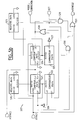
- the correction circuit 207 illustrated in FIG. 5b comprises an 8-bit register 520, a 8-bit counter 521 and an 8-bit comparator 522.
- the output OUT ⁇ 7: 0> of register 520 is connected to the input IN ⁇ 7: 0> of the counter 520, and vice versa.
- the output OUT ⁇ 7: 0> of counter 521 is connected to input IN ⁇ 7: 0> of comparator 522.
- the input LOAD from register 520 and Rin input from counter 521 are connected to ground.
- Circuit 5b also includes a register 3 bits 523, a 3-bit counter 524 and a comparator 3 bits 525.
- the output OUT ⁇ 2: 0> of the register 523 is connected to input IN ⁇ 2: 0> of the counter 524, and vice versa.
- the exit OUT ⁇ 2: 0> of counter 524 is connected to input IN ⁇ 2: 0> of comparator 525.
- the LOAD entry of register 523 and the Rin input of the 524 counter are connected to ground.
- Register 520 contains the minimum number of lines occupied by signaling whatever the standard. In addition, register 523 contains the number 0.
- LOAD inputs of counters 521 and 524 receive the vertical synchronization signal VSYNCI while the CLK inputs receive the signal HSYNCI horizontal synchronization.
- the output of OR gate 528 is connected on the one hand to the CE validation input of counter 524 and on the other hand to a first entry an ET 529 door.
- This ET 529 door also receives on a second input the detection signal DET signaling pulse delivered by the circuit horizontal synchronization correction 205 and, on a third input a correction signal MODE_CORRECTION.
- the MODE_CORRECTION signal allows trigger the operation of the correction circuit 207.
- this correction signal attacks a second entry of the door ET 530.
- the exit of the doors 529 and 530 are connected respectively to a first and at a second entrance to an OR 531 door. last also receives on a third entry the horizontal synchronization signal VSYNCI and delivers as output the vertical synchronization signal corrected VSYNCO2.
- Register 520 is preloaded with the number minimum of lines used for signaling in the different standards which represent the fixed part of the extension of the frame return pulse. In our example this value is equal to 6. By the way, register 523 contains the value 0.
- circuit 207 The operation of circuit 207 is as follows: the end of the frame return pulse of the VSYNCI signal, counter 521 starts to count down from the starting value contained in register 520. During the countdown of the counter 521, the output signal VSYNCO2 is kept at 1. In the example of the figure 6, the frame return pulse is extended automatically 6 lines. Then the counter 524 starts to count down when the output OUT ⁇ 7: 0> of the counter 521 is equal to 1. Counter 524 goes to 7 when counter 521 goes to 0. As long as the state of counter 521 is not equal to 0 and that the signal DET is at 1, the output signal VSYNCO2 is maintained at 1.
- diagrams illustrated are 3b and 4b were made with elements using 11-bit data. In practice, they can be made from elements working with 8-bit data in series with elements working with 3-bit data, so optimize the final circuit diagram synchronization 201 using the same elements for circuits 205, 206 and 207.
- circuit synchronization 201 the same elements are used for the three circuits 202, 203 and 204 dealing with horizontal synchronization. So is even for circuits 205, 206 and 207.
- a microprocessor not described in the figures, allows then organize the connections between these different elements depending on the use of the circuit synchronization.
Landscapes
- Engineering & Computer Science (AREA)
- Multimedia (AREA)
- Signal Processing (AREA)
- Synchronizing For Television (AREA)
Description
- un circuit de génération de synchronisation horizontale pour produire un premier signal de sortie de synchronisation horizontale à partir du signal d'horloge, et
- un circuit de génération de synchronisation verticale pour produire un premier signal de sortie de synchronisation verticale à partir du premier signal de sortie de synchronisation horizontale,
- un circuit d'analyse de synchronisation horizontale, recevant en entrée le signal d'entrée de synchronisation horizontale et le signal d'horloge, et produisant une valeur représentative de l'intervalle de temps entre deux impulsions de synchronisation de ligne du signal d'entrée de synchronisation horizontale,
- un circuit de correction de synchronisation horizontale délivrant un second signal de sortie de synchronisation horizontale dépourvu d'impulsions du deuxième type en fin de trame et un signal de détection d'impulsion de signalisation, à partir dudit signal d'entrée de synchronisation horizontale, du signal d'horloge et de la valeur représentative de l'intervalle de temps entre deux impulsions de synchronisation de ligne du signal d'entrée de synchronisation horizontale,
- un circuit d'analyse de synchronisation verticale, recevant en entrée ledit signal d'entrée de synchronisation verticale et le signal d'entrée de synchronisation horizontale, et produisant une valeur représentative du nombre de lignes entre deux impulsions de retour trame du signal d'entrée de synchronisation verticale, et
- un circuit de correction de synchronisation verticale délivrant un second signal de sortie de synchronisation verticale dont l'impulsion de retour de trame est prolongée pendant les impulsions de signalisation du premier type en début de trame, à partir dudit signal d'entrée de synchronisation verticale, du signal d'entrée de synchronisation horizontale et du signal de détection d'impulsion de signalisation.
- le circuit de génération de synchronisation horizontale peut comporter un premier registre dans lequel est mémorisée une valeur représentative de la période du premier signal de sortie de synchronisation horizontale;
- le circuit d'analyse de synchronisation horizontale peut comporter un circuit pour mesurer l'intervalle de temps entre deux impulsions de synchronisation de ligne du signal de synchronisation horizontale et un deuxième registre pour mémoriser la valeur représentative dudit intervalle de temps;
- le circuit de correction de synchronisation horizontale peut comporter un circuit pour produire le second signal de sortie de synchronisation horizontale ne comprenant pas pas le deuxième type d'impulsion de signalisation en fin de trame;
- le circuit de correction de synchronisation horizontale peut comporter un circuit pour détecter le premier et le deuxième type d'impulsion de signalisation délivrant le signal de détection d'impulsion de signalisation;
- le circuit de correction de synchronisation horizontale peut comporter un troisième registre dans lequel est mémorisée la valeur représentative de l'intervalle de temps entre deux impulsions de synchronisation de ligne du signal de synchronisation horizontale;
- le circuit de génération de synchronisation verticale peut comporter un quatrième registre dans lequel est mémorisée une valeur égale au nombre de lignes pendant une période du premier signal de sortie de synchronisation verticale;
- le circuit d'analyse de synchronisation verticale peut comporter un circuit pour mesurer un nombre de lignes entre deux impulsions de retour trame du signal d'entrée de synchronisation verticale et un cinquième registre pour mémoriser la valeur représentative dudit nombre de lignes;
- le circuit de correction de synchronisation verticale peut comporter un circuit pour produire le second signal de sortie de synchronisation verticale dont les impulsions de retour trame sont prolongées pendant les impulsions de signalisation du premier type du signal d'entrée de synchronisation horizontale.
- la figure 1, un diagramme temporel de signaux de synchronisation horizontale et verticale,
- la figure 2, un schéma fonctionnel d'un circuit de synchronisation selon l'invention,
- la figure 3a, une réalisation particulière du circuit de génération de synchronisation horizontale selon l'invention,
- la figure 3b, une réalisation particulière du circuit de génération de synchronisation verticale selon l'invention,
- la figure 4a, une réalisation particulière du circuit d'analyse de synchronisation horizontale selon l'invention,
- la figure 4b, une réalisation particulière du circuit d'analyse de synchronisation verticale selon l'invention,
- la figure 5a, une réalisation particulière du circuit de correction de synchronisation horizontale selon l'invention,
- la figure 5b, une réalisation particulière du circuit de correction de synchronisation verticale selon l'invention, et
- la figure 6, un chronogramme des principaux signaux intervenant dans le fonctionnement du circuit de correction de synchronisation verticale.
- un circuit de génération de synchronisation horizontale 202 recevant un signal d'horloge CLK et délivrant un premier signal de sortie de synchronisation horizontale HSYNCO1,
- un circuit d'analyse de synchronisation horizontale 203, recevant en entrée le signal d'entrée de synchronisation horizontale HSYNCI et le signal d'horloge CLK, et produisant une valeur VAL1 représentative de l'intervalle de temps entre deux impulsions de synchronisation de ligne du signal d'entrée de synchronisation horizontale HSYNCI,
- un circuit de correction de synchronisation horizontale 204 délivrant un second signal de sortie de synchronisation horizontale HSYNCO2 et un signal de détection d'impulsion de signalisation DET, à partir dudit signal d'entrée de synchronisation horizontale HSYNCI, du signal d'horloge CLK et de la valeur VAL1 représentative de l'intervalle de temps entre deux impulsions de synchronisation de ligne du signal d'entrée de synchronisation horizontale,
- un circuit de génération de synchronisation verticale 205 pour produire un premier signal de sortie de synchronisation verticale VSYNCO1 à partir du premier signal de sortie de synchronisation horizontale HSYNCO1,
- un circuit d'analyse de synchronisation verticale 206, recevant en entrée le signal d'entrée de synchronisation verticale VSYNCI et le signal d'entrée de synchronisation horizontale HSYNCI, et produisant une valeur VAL2 représentative du nombre de lignes entre deux impulsions de retour trame du signal d'entrée de synchronisation verticale, et
- un circuit de correction de synchronisation verticale 207 délivrant un second signal de sortie de synchronisation verticale VSYNCO2, à partir dudit signal d'entrée de synchronisation verticale VSYNCI, du signal d'entrée de synchronisation horizontale HSYNCI et du signal de détection d'impulsion de signalisation DET.
Claims (10)
- Circuit de synchronisation (201) pour écrans à circuit de balayage recevant un signal d'entrée de synchronisation horizontale (HSYNCI) comportant des impulsions de synchronisation de ligne (102), un premier type d'impulsion de signalisation (103) en début de trame et un deuxième type d'impulsion de signalisation (104) en fin de trame, un signal d'entrée de synchronisation verticale (VSYNCI) comportant des impulsions de retour trame (100), et un signal d'horloge (CLK), lequel circuit de synchronisation comporte:et est caractérisé en ce qu'il comporte:un circuit de génération de synchronisation horizontale (202) pour produire un premier signal de sortie de synchronisation horizontale (HSYNCO1) à partir du signal d'horloge (CLK), etun circuit de génération de synchronisation verticale (205) pour produire un premier signal de sortie de synchronisation verticale (VSYNCO1) à partir du premier signal de sortie de synchronisation horizontale (HSYNCO1),un circuit d'analyse de synchronisation horizontale (203) , recevant en entrée le signal d'entrée de synchronisation horizontale (HSYNCI) et le signal d'horloge (CLK), et produisant une valeur (VAL1) représentative de l'intervalle de temps entre deux impulsions de synchronisation de ligne du signal d'entrée de synchronisation horizontale (HSYNCI),un circuit de correction de synchronisation horizontale (204) délivrant un second signal de sortie de synchronisation horizontale dépourvu d'impulsions du deuxième type en fin de trame (HSYNCO2) et un signal de détection d'impulsion de signalisation (DET), à partir dudit signal d'entrée de synchronisation horizontale (HSYNCI), du signal d'horloge (CLK) et de la valeur (VAL1) représentative de l'intervalle de temps entre deux impulsions de synchronisation de ligne du signal d'entrée de synchronisation horizontale,un circuit d'analyse de synchronisation verticale (206), recevant en entrée ledit signal d'entrée de synchronisation verticale (VSYNCI) et le signal d'entrée de synchronisation horizontale (HSYNCI), et produisant une valeur (VAL2) représentative du nombre de lignes entre deux impulsions de retour trame du signal d'entrée de synchronisation verticale (VSYNCI), etun circuit de correction de synchronisation verticale (207) délivrant un second signal de sortie de synchronisation verticale (VSYNCO2) dont l'impulsion de retour de trame est prolongée pendant les impulsions de signalisation du premier type en début de trame, à partir dudit signal d'entrée de synchronisation verticale (VSYNCI), du signal d'entrée de synchronisation horizontale (HSYNCI) et du signal de détection d'impulsion de signalisation (DET).
- Circuit selon la revendication 1, caractérisé en ce que le circuit de génération de synchronisation horizontale (202) comporte un premier registre (301) dans lequel est mémorisée une valeur représentative de la période du premier signal de sortie de synchronisation horizontale (HSYNCO1).
- Circuit selon l'une des revendications 1 à 2, caractérisé en ce que le circuit d'analyse de synchronisation horizontale (203) comporte un circuit (402-413) pour mesurer l'intervalle de temps entre deux impulsions de synchronisation de ligne du signal de synchronisation horizontale (HSYNCI) et un deuxième registre (401) pour mémoriser la valeur (VAL1) représentative dudit intervalle de temps.
- Circuit selon l'une des revendications 1 à 3, caractérisé en ce que le circuit de correction de synchronisation horizontale (204) comporte un circuit (501-516) pour produire le second signal de sortie de synchronisation horizontale (HSYNCO2) ne comprenant pas pas le deuxième type d'impulsion de signalisation (104) en fin de trame.
- Circuit selon l'une des revendications 1 à 4, caractérisé en ce que le circuit de correction de synchronisation horizontale (204) comporte un circuit (517-519) pour détecter le premier et le deuxième type d'impulsion de signalisation (103 et 104) délivrant le signal de détection d'impulsion de signalisation (DET).
- Circuit selon la revendication 3 et la revendication 4, caractérisé en ce que le circuit de correction de synchronisation horizontale (204) comporte un troisième registre (501) dans lequel est mémorisée la valeur (VAL1) représentative de l'intervalle de temps entre deux impulsions de synchronisation de ligne du signal de synchronisation horizontale (HSYNCI).
- Circuit selon l'une des revendications 1 à 6, caractérisé en ce que le circuit de génération de synchronisation verticale (205) comporte un quatrième registre (306) dans lequel est mémorisée une valeur égale au nombre de lignes pendant une période du premier signal de sortie de synchronisation verticale (VSYNCO1).
- Circuit selon l'une des revendications 1 à 7, caractérisé en ce que le circuit d'analyse de synchronisation verticale (206) comporte un circuit (416-427) pour mesurer un nombre de lignes entre deux impulsions de retour trame du signal d'entrée de synchronisation verticale (VSYNCI) et un cinquième registre (415) pour mémoriser la valeur (VAL2) représentative dudit nombre de lignes.
- Circuit selon l'une des revendications 1 à 8, caractérisé en ce que le circuit de correction de synchronisation verticale (207) comporte un circuit (520-535) pour produire le second signal de sortie de synchronisation verticale (VSYNCO2) dont les impulsions de retour trame sont prolongées pendant les impulsions de signalisation du premier type (103) du signal d'entrée de synchronisation horizontale (HSYNCI).
- Utilisation d'un circuit de synchronisation (201) selon l'une des revendications 1 à 9 dans un moniteur de télévision.
Applications Claiming Priority (2)
| Application Number | Priority Date | Filing Date | Title |
|---|---|---|---|
| FR9512611 | 1995-10-20 | ||
| FR9512611A FR2740288B1 (fr) | 1995-10-20 | 1995-10-20 | Circuit de synchronisation |
Publications (2)
| Publication Number | Publication Date |
|---|---|
| EP0769870A1 EP0769870A1 (fr) | 1997-04-23 |
| EP0769870B1 true EP0769870B1 (fr) | 1998-12-23 |
Family
ID=9483923
Family Applications (1)
| Application Number | Title | Priority Date | Filing Date |
|---|---|---|---|
| EP96460034A Expired - Lifetime EP0769870B1 (fr) | 1995-10-20 | 1996-10-15 | Circuit de synchronisation |
Country Status (4)
| Country | Link |
|---|---|
| US (1) | US6052153A (fr) |
| EP (1) | EP0769870B1 (fr) |
| DE (1) | DE69601205T2 (fr) |
| FR (1) | FR2740288B1 (fr) |
Families Citing this family (1)
| Publication number | Priority date | Publication date | Assignee | Title |
|---|---|---|---|---|
| JP3998410B2 (ja) * | 2000-11-02 | 2007-10-24 | 三菱電機株式会社 | 同期回路 |
Family Cites Families (7)
| Publication number | Priority date | Publication date | Assignee | Title |
|---|---|---|---|---|
| GB2094083B (en) * | 1981-02-20 | 1984-10-10 | Tokyo Shibaura Electric Co | An equalizing pulse removal circuit |
| JPS632468A (ja) * | 1986-06-20 | 1988-01-07 | Mitsubishi Electric Corp | 同期分離回路 |
| JPH02135995A (ja) * | 1988-11-17 | 1990-05-24 | Sony Corp | テレビジョン受像機 |
| JPH071423B2 (ja) * | 1988-12-20 | 1995-01-11 | 株式会社山下電子設計 | パルス発生回路 |
| JP2766547B2 (ja) * | 1990-08-08 | 1998-06-18 | シャープ株式会社 | 水平同期信号分離回路 |
| US5126639A (en) * | 1991-06-04 | 1992-06-30 | Zenith Electronics Corporation | Sequential scan system changes for multiple frequency range oscillator and control |
| KR950003024B1 (ko) * | 1992-02-29 | 1995-03-29 | 삼성전자 주식회사 | 동기신호 발생장치 |
-
1995
- 1995-10-20 FR FR9512611A patent/FR2740288B1/fr not_active Expired - Fee Related
-
1996
- 1996-10-15 DE DE69601205T patent/DE69601205T2/de not_active Expired - Fee Related
- 1996-10-15 EP EP96460034A patent/EP0769870B1/fr not_active Expired - Lifetime
- 1996-10-18 US US08/734,524 patent/US6052153A/en not_active Expired - Lifetime
Also Published As
| Publication number | Publication date |
|---|---|
| DE69601205T2 (de) | 1999-05-20 |
| US6052153A (en) | 2000-04-18 |
| FR2740288B1 (fr) | 1997-12-05 |
| DE69601205D1 (de) | 1999-02-04 |
| FR2740288A1 (fr) | 1997-04-25 |
| EP0769870A1 (fr) | 1997-04-23 |
Similar Documents
| Publication | Publication Date | Title |
|---|---|---|
| US12078720B2 (en) | Systems, methods, and media for single photon depth imaging with improved precision in ambient light | |
| FR2514900A1 (fr) | Dispositif de memorisation et de visualisation de formes d'onde | |
| US11448767B2 (en) | Systems, methods, and media for asynchronous single photon depth imaging with improved precision in ambient light | |
| FR2482814A1 (fr) | Procede et dispositif pour coder et decoder des signaux video par inversion repetitive de la polarite de ces signaux | |
| FR2598570A1 (fr) | Circuit retardateur numerique | |
| EP4674132A1 (fr) | Procédé et système d'imagerie monophotonique | |
| CA2017802C (fr) | Dispositif de detection de perte de signal de reception pour recepteur de signaux numeriques | |
| FR2543770A1 (fr) | Procede et systeme de condensation de donnees d'images binaires | |
| EP1300660B1 (fr) | Correlateur de photons | |
| FR2482395A1 (fr) | Eliminateur de signaux d'image fantome pour televiseur | |
| FR2716765A1 (fr) | Procédé de reconnaisance de standard vidéo, et circuit mettant en Óoeuvre ce procédé. | |
| EP0355919B1 (fr) | Dispositif de sychronisation sur des paquets de données numériques et lecteur le comprenant | |
| EP1101316B1 (fr) | Procede de recuperation d'horloge lors de l'echantillonnage de signaux de type numerique | |
| EP0769870A1 (fr) | Circuit de synchronisation | |
| EP0821488B1 (fr) | Dispositif de sélection de fréquence muni d'un détecteur de verrouillage | |
| EP0781038B1 (fr) | Dispostitif de traitement de signaux de synchronisation | |
| EP0384536A1 (fr) | Procédé et dispositif de synchronisation bit dans un récepteur de transmission de données numériques | |
| FR2680058A1 (fr) | Procede et dispositif de synchronisation d'un signal. | |
| EP0052863B1 (fr) | Dispositif d'adressage d'un ensemble d'enregistreurs d'un central de commutation | |
| JPH05281038A (ja) | パルスレーザ光の光強度分布測定装置 | |
| EP0312449B1 (fr) | Dispositif de contrôle de présence d'informations d'images dans des signaux vidéo | |
| FR2553517A1 (fr) | Appareil collecteur de donnees ultrasonores pour formation d'images | |
| FR2841723A1 (fr) | Procede et circuit d'extraction de signaux de synchronisation dans un signal video | |
| FR2586152A1 (fr) | Systeme analyseur digital pour mesurer et controler des parametres de synchronisation d'un signal de video couleur | |
| EP0350361A1 (fr) | Dispositif d'évaluation de la marge de tolérance d'un signal vidéo numérique |
Legal Events
| Date | Code | Title | Description |
|---|---|---|---|
| PUAI | Public reference made under article 153(3) epc to a published international application that has entered the european phase |
Free format text: ORIGINAL CODE: 0009012 |
|
| AK | Designated contracting states |
Kind code of ref document: A1 Designated state(s): DE FR GB IT |
|
| 17P | Request for examination filed |
Effective date: 19970910 |
|
| 17Q | First examination report despatched |
Effective date: 19971031 |
|
| GRAG | Despatch of communication of intention to grant |
Free format text: ORIGINAL CODE: EPIDOS AGRA |
|
| GRAG | Despatch of communication of intention to grant |
Free format text: ORIGINAL CODE: EPIDOS AGRA |
|
| GRAH | Despatch of communication of intention to grant a patent |
Free format text: ORIGINAL CODE: EPIDOS IGRA |
|
| GRAH | Despatch of communication of intention to grant a patent |
Free format text: ORIGINAL CODE: EPIDOS IGRA |
|
| GRAA | (expected) grant |
Free format text: ORIGINAL CODE: 0009210 |
|
| AK | Designated contracting states |
Kind code of ref document: B1 Designated state(s): DE FR GB IT |
|
| RAP4 | Party data changed (patent owner data changed or rights of a patent transferred) |
Owner name: STMICROELECTRONICS S.A. |
|
| REF | Corresponds to: |
Ref document number: 69601205 Country of ref document: DE Date of ref document: 19990204 |
|
| GBT | Gb: translation of ep patent filed (gb section 77(6)(a)/1977) |
Effective date: 19990115 |
|
| ITF | It: translation for a ep patent filed | ||
| PLBE | No opposition filed within time limit |
Free format text: ORIGINAL CODE: 0009261 |
|
| STAA | Information on the status of an ep patent application or granted ep patent |
Free format text: STATUS: NO OPPOSITION FILED WITHIN TIME LIMIT |
|
| 26N | No opposition filed | ||
| REG | Reference to a national code |
Ref country code: GB Ref legal event code: IF02 |
|
| PGFP | Annual fee paid to national office [announced via postgrant information from national office to epo] |
Ref country code: DE Payment date: 20041007 Year of fee payment: 9 |
|
| PGFP | Annual fee paid to national office [announced via postgrant information from national office to epo] |
Ref country code: FR Payment date: 20050825 Year of fee payment: 10 |
|
| PGFP | Annual fee paid to national office [announced via postgrant information from national office to epo] |
Ref country code: GB Payment date: 20051012 Year of fee payment: 10 |
|
| PG25 | Lapsed in a contracting state [announced via postgrant information from national office to epo] |
Ref country code: IT Free format text: LAPSE BECAUSE OF NON-PAYMENT OF DUE FEES;WARNING: LAPSES OF ITALIAN PATENTS WITH EFFECTIVE DATE BEFORE 2007 MAY HAVE OCCURRED AT ANY TIME BEFORE 2007. THE CORRECT EFFECTIVE DATE MAY BE DIFFERENT FROM THE ONE RECORDED. Effective date: 20051015 |
|
| PG25 | Lapsed in a contracting state [announced via postgrant information from national office to epo] |
Ref country code: DE Free format text: LAPSE BECAUSE OF NON-PAYMENT OF DUE FEES Effective date: 20060503 |
|
| GBPC | Gb: european patent ceased through non-payment of renewal fee |
Effective date: 20061015 |
|
| REG | Reference to a national code |
Ref country code: FR Ref legal event code: ST Effective date: 20070629 |
|
| PG25 | Lapsed in a contracting state [announced via postgrant information from national office to epo] |
Ref country code: GB Free format text: LAPSE BECAUSE OF NON-PAYMENT OF DUE FEES Effective date: 20061015 |
|
| PG25 | Lapsed in a contracting state [announced via postgrant information from national office to epo] |
Ref country code: FR Free format text: LAPSE BECAUSE OF NON-PAYMENT OF DUE FEES Effective date: 20061031 |