EP0764300B1 - Übertragvorgriffsgerät mit alternierender polarität - Google Patents
Übertragvorgriffsgerät mit alternierender polarität Download PDFInfo
- Publication number
- EP0764300B1 EP0764300B1 EP96911645A EP96911645A EP0764300B1 EP 0764300 B1 EP0764300 B1 EP 0764300B1 EP 96911645 A EP96911645 A EP 96911645A EP 96911645 A EP96911645 A EP 96911645A EP 0764300 B1 EP0764300 B1 EP 0764300B1
- Authority
- EP
- European Patent Office
- Prior art keywords
- source
- drain
- gate
- carry
- input terminal
- Prior art date
- Legal status (The legal status is an assumption and is not a legal conclusion. Google has not performed a legal analysis and makes no representation as to the accuracy of the status listed.)
- Expired - Lifetime
Links
Images


Classifications
-
- G—PHYSICS
- G06—COMPUTING OR CALCULATING; COUNTING
- G06F—ELECTRIC DIGITAL DATA PROCESSING
- G06F7/00—Methods or arrangements for processing data by operating upon the order or content of the data handled
- G06F7/38—Methods or arrangements for performing computations using exclusively denominational number representation, e.g. using binary, ternary, decimal representation
- G06F7/48—Methods or arrangements for performing computations using exclusively denominational number representation, e.g. using binary, ternary, decimal representation using non-contact-making devices, e.g. tube, solid state device; using unspecified devices
- G06F7/50—Adding; Subtracting
- G06F7/505—Adding; Subtracting in bit-parallel fashion, i.e. having a different digit-handling circuit for each denomination
- G06F7/506—Adding; Subtracting in bit-parallel fashion, i.e. having a different digit-handling circuit for each denomination with simultaneous carry generation for, or propagation over, two or more stages
- G06F7/508—Adding; Subtracting in bit-parallel fashion, i.e. having a different digit-handling circuit for each denomination with simultaneous carry generation for, or propagation over, two or more stages using carry look-ahead circuits
-
- G—PHYSICS
- G06—COMPUTING OR CALCULATING; COUNTING
- G06F—ELECTRIC DIGITAL DATA PROCESSING
- G06F7/00—Methods or arrangements for processing data by operating upon the order or content of the data handled
- G06F7/38—Methods or arrangements for performing computations using exclusively denominational number representation, e.g. using binary, ternary, decimal representation
- G06F7/48—Methods or arrangements for performing computations using exclusively denominational number representation, e.g. using binary, ternary, decimal representation using non-contact-making devices, e.g. tube, solid state device; using unspecified devices
- G06F7/50—Adding; Subtracting
Definitions
- the present invention relates to binary adders for integrated circuits. Specifically, the present invention relates to carry look ahead adders in which propagation delay and hardware costs are minimized.
- Figure 1 illustrates a standard ripple carry adder structure.
- the ripple carry adder takes two binary numbers, A and B, as inputs, and produces a single binary number, S, as output.
- A, B, and S are each six bits in length.
- the ripple carry adder in Figure 1 is made of six full adder cells 100. Although the ripple carry adder is implemented with a minimal amount of hardware, its propagation delay is relatively large. Each full adder 100 takes a carry input C in which is necessary to compute its sum output and carry output C out . The amount of time necessary for the most significant bit S 5 of the output S and the carry output C 6 to become valid is constrained by the possibility of an asserted carry signal rippling through the row of adders from C 0 to C 6 .
- each full adder cell 100 requires a time t c to compute the C out output after the C in input has become valid, then the total propagation delay of the adder shown in Figure 1 is 6*t c .
- the propagation delay is approximately n*t c for a ripple carry adder, where n is the number of full adders in the circuit. Therefore, the growth of the propagation delay of the ripple carry adder is a linear function of the number of bits in the addends.
- FIG. 2 shows the structure of a 6-bit carry look ahead adder.
- the 6-bit adder in Figure 2 has two stages 200 & 201 of three-level look ahead circuits.
- Each three-level look ahead circuit 200 & 201 directly computes its C out output based upon the appropriate six bits of the addends-three bits from A and three bits from B--and its carry input C in .
- a carry look ahead adder is typically designed so that the latency of the computation of C out after its C in input becomes valid has the same order of latency as each full adder cell 203.
- the full adder cells 204 computing the more significant bits of the adder's output receive their carry inputs earlier than in a similar ripple carry adder so that the most latent outputs, S 5 and C 6 , become valid with less latency.
- C i G i + P i ⁇ C i-1
- G i A i ⁇ B i
- P i A i + B i
- G i is the generate signal, which indicates that the addition of A i and B i will generate a carry output from the i th full adder.
- P i is the propagate signal, which indicates that any carry input to the i th full adder cell will be propagated to the carry output.
- C i G i + P i ⁇ G i-1 + P i ⁇ P i-1 ⁇ G i-2 + ... + P i ...P 1 ⁇ C 0
- the amount of hardware necessary to implement m stages of a k-level carry look ahead circuit is always less than the amount of hardware necessary to implement a single stage of k*m-level carry look ahead circuit.
- This inequality is a result of the fact that the complexity of the computation of C out increases polynomially as k increases. Therefore, the amount of hardware necessary to make a k-level carry look ahead circuit can clearly get out of hand when k becomes too large. As a result, the number of levels of look ahead is usually limited to about six.
- carry add select circuit One way to implement a carry look ahead circuit with very little delay through the critical path from carry in to carry out is the carry add select circuit.
- the carry add select circuit as shown in Figure 3, two separate carry computation circuits 300 & 301 are used to speculatively calculate both possible carry outputs C out0 and C out1 based upon the two possible carry input values, zero or one.
- the advantage to this approach is that the speculative computations of the two possible carry outputs C out0 and C out1 begin before the carry input C in 302 has been computed by the preceding look ahead stage.
- the correct output 303 is selected from among the two speculatively computed possibilities, C out0 and C out1 , by the multiplexor 304. Therefore, the propagation delay for the carry look ahead stage is merely the delay from the select input 305 to the output 303 of the multiplexor.
- Any given multiplexor implementation requires at least two logic levels; therefore. a minimum of two gate delays are required to implement a multiplexor.
- a multiplexor circuit employs either two inverting gates or two transmission gates.
- Figures 4A and 4B show two alternative implementations of the multiplexor 304 shown in Figure 3. Either implementation has substantially larger delays than a single inverting gate.
- Equation 4 For a k-bit carry look ahead adder circuit, the fundamental Equation 4 can be written in the following form.
- C k is the carry output of the k-bit carry look ahead adder circuit
- C 0 is the carry input.
- Previous implementations of a carry look ahead circuit preserve the polarity from the carry input C 0 , to the carry output C k , as indicated in Equation 6. In other words, both the carry input C 0 and the carry output C k are represented using positive logic according to the prior art.
- Figures 5A and 5B show typical logic circuits which performs the computation of C k from C 0 , P, and G as described by Equation 6. Similar to the carry add select circuit, the typical logic circuit shown in Figures 5B attempt to minimize the delay from the input C 0 to the output C k . Depending upon the number of levels of look ahead (k), the generation of P and G can become complex computations involving only k bits of A and k bits of B, but not involving carry information from previous stages. Therefore, the computations of P and G in any given carry look ahead stage begin immediately, and are designed so as to finish before C 0 becomes valid, so that the path from C 0 to C k is the critical path. The logic implementation shown in Figure 5B clearly requires two gate delays.
- EP-A-0442665 which describes a 'universal' look-ahead stage having features corresponding to those in the precharacterising part of claim 1.
- EP 590251 discloses an apparatus that performs carry look ahead computations, operating on pair operand pairs.
- the invention provides apparatus that performs carry look ahead computations in a binary adder, the apparatus comprising: a carry input terminal that receives a carry input signal having a first logical polarity; a first pair of addend input terminals that receive a first pair of addend bits having the first logical polarity; a second pair of addend input terminals that receive a second pair of addend bits having the first logical polarity; an output terminal that supplies a carry output signal having a second logical polarity; and a logic gate circuit taking the carry input signal and the first and second pairs of addend bits as inputs and directly computing the carry output signal; such that the carry output signal is asserted when an arithmetic addition of the first and second pairs of addend bits and the carry input signal produces a resulting sum requiring one more bit in order to represent the resulting sum than is present in either the first or second pairs of addend bits; wherein the first pair of addend input terminals includes a first low order input terminal and a first high order input terminal; the second
- the logic gate circuit preferably further comprises: a multiplicity of p-channel transistors, these transistors having respectively the tenth source, gate and drain to the eighteenth source gate and drain; wherein the tenth source is connected to the eleventh drain, the eleventh drain is connected to the tenth source, and the eleventh gate is connected to the first low order input terminal; the twelfth source is connected to the thirteenth drain, the twelfth drain is connected to the tenth source, and the twelfth gate is connected to the second low order input terminal; the thirteenth source is connected to a high supply voltage, the thirteenth drain is connected to the twelfth source, and the thirteenth gate is connected to the first high order input terminal; the fourteenth source is connected to the high supply voltage, the fourteenth drain is connected to the eleventh source, and the fourteenth gate is connected to the second high order input terminal; the fifteenth source is connected to the sixteenth drain, the fifteenth drain is connected to the output terminal, and the fifteenth gate is connected to the first low
- a second significant advantage of the present invention is that the minimum achievable propagation delay through an alternating polarity carry look ahead adder is less than with prior art carry look ahead adders.
- a carry look ahead adder is designed so that the carry chain is the critical path. Because the delay from carry input to carry output in each alternating polarity carry look ahead stage is less than with conventional look ahead adder stages, the critical path of the overall adder will be correspondingly lower.
- Figure 1 illustrates a conventional 6-bit ripple carry binary adder.
- Figure 2 illustrates a conventional 6-bit carry look ahead adder having two stages of three-level look ahead circuits.
- Figure 3 illustrates a conventional carry add select implementation of carry look ahead circuit.
- Figure 4A illustrates a conventional CMOS transmission gate implementation of the multiplexor circuit shown in Figure 3.
- Figure 4B illustrates another implementation of a multiplexor circuit as shown in Figure 3.
- Figure 5A illustrates one implementation of the logic in a conventional carry look ahead adder circuit's critical path.
- Figure 5B illustrates a second possible implementation of a conventional carry look ahead adder circuit's critical path.
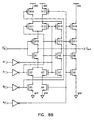
- Figure 6 illustrates a 12-bit carry look ahead adder using carry look ahead circuits according to the present invention.
- Figure 7A illustrates a CMOS implementation of an odd carry look ahead circuit stage.
- Figure 7B illustrates a CMOS implementation of an even carry look ahead circuit stage.
- Figure 8A illustrates a CMOS implementation of an odd 2-level carry look ahead circuit stage according to an embodiment of the present invention.
- Figure 8B illustrates a CMOS implementation of an even 2-level carry look ahead circuit stage according to an embodiment of the present invention.
- Figure 9 illustrates one possible partitioning of a carry look ahead adder using carry look ahead circuits according to the present invention in which the adder is structured so as to be optimized for minimum propagation delay.
- a carry look ahead circuit is implemented such that only one gate delay is incurred in calculating the carry output C out after the carry input C in becomes valid.
- Carry look ahead circuits according to the present invention are referred to as having alternating polarity.
- C k G + P ⁇ C 0
- P P k ...P 1
- G G k + P k ⁇ G k-1 + P k ⁇ P k-1 ⁇ G k-2 + ... + P k ...P 2 ⁇ G 1
- Each carry look ahead circuit 600 & 601 has an output C k and a carry input C 0 .
- the following equations represent the logic definitions for the carry input and the carry output of "odd" look ahead stages according to the present invention.
- the slash represents logical negation, and indicates that the output /C out is defined using negative logic.
- the logic equation for odd stages of carry look ahead is derived.
- /C out G + P ⁇ C in For these odd stages.
- the output /C out is asserted when zero and is deasserted when one, while the input C in is asserted when one and deasserted when zero.
- the input C in is represented using positive logic
- the output /C out is represented using negative logic.
- Figures 7A and 7B depict separate CMOS implementations of the odd and even stages.
- Figures 7A and 7B implement Equations 16 and 19, respectively.
- the generate-propagate blocks 700 perform the computations of the G and P terms defined by Equations 10 through 13 and used in Equations 16 and 19, respectively.
- Both these circuits in Figures 7A and 7B can be used for any level k of look ahead. As k increases, the complexity of the generate-propagate blocks 700 increases, but the remainder of the circuits shown in Figures 7A and 7B are unaffected. Therefore, the implementation depicted in Figures 7A and 7B is applicable for any level k of look ahead.
- the circuit in Figure 7A does not incur an inversion in producing its output /C out . From C in to /C out , therefore only a single gate delay is incurred. This reduces the length of the critical path from C in to /C out by nearly a factor of two over the prior art equivalent path from C in to C out .
- the circuit shown in Figure 7B illustrates a CMOS implementation of an even stage.
- the even stage also has only a single gate delay from input /C in to output C out .
- the structure of the even stage is very similar to the structure of the odd stage; by interchanging V dd and ground, interchanging P-channel and N-channel devices, and inverting the polarities of all inputs and outputs, the odd stage shown in Figure 7A is transformed into the even stage shown in Figure 7B.
- the generate and propagate signal computations are integrated into the complex gate which produces the carry output of each carry look ahead stage.
- Figures 8A and 8B show optimized CMOS circuits implementing 2-level alternating polarity carry look ahead adder stages according to the present invention.
- the generate and propagate signal computations are integrated into one complex gate which performs the C out computation. In this manner, a reduction in the number of transistors used and circuit complexity can be achieved by implementing the propagate and generate logic directly into the carry look ahead circuit.
- Equation 8B has the same structure as equation 8A, with inverted data inputs.
- the corresponding implementation is shown in Figure 8B, and indeed is the same structure as Figure 8A.
- a 16-bit parallel adder using 8 stages of this alternating polarity 2-level carry look ahead circuit implementation had approximately the same propagation delay as 4 stages of 4-level conventional carry look ahead, but with a substantial reduction in circuit complexity. This same strategy can be applied to levels of look ahead greater than 2 using similar derivations, but are omitted from discussion for the sake of brevity.
- the present invention Using the present invention, less hardware is required to implement an adder circuit having a predetermined propagation delay than is required using prior art approaches.
- the present invention eliminates an inverter from each stage; however, the bulk of the savings occurs in the generate and propagate computations.
- the critical path of any properly designed adder is through the carry chain. Normally, the number of levels of look ahead, k, is increased in order to reduce the propagation delay through the critical path.
- the amount of hardware necessary to implement the generate (G) and propagate (P) signals (700 in Figures 7A and 7B) for each carry look ahead circuit increases polynomially as k is increased.
- a k-level carry look ahead circuit according to the present invention will have roughly half the delay as a conventional prior art k-level carry look ahead circuit.
- a conventional carry look ahead adder designed such that two 16-bit binary numbers are added together using 4 levels of 4-stage carry look ahead
- the resulting propagation delay is t, for example.
- 8 levels of alternating polarity 2-level carry look ahead can be used, because the alternating polarity carry look ahead circuits have approximately half the delay as conventional carry look ahead circuits.
- the hardware required to implement 8 levels of alternating polarity 2-level carry look ahead is significantly less than 4 stages of conventional 4-level carry look ahead.
- a second significant advantage of the present invention is that the minimum achievable propagation delay through an alternating polarity carry look ahead adder is less than with prior art carry look ahead adders.
- a carry look ahead adder is designed so that the carry chain is the critical path.
- the number of levels of look ahead can be designed so as to increase with each successive stage. This allows the computations of the generate and propagate signals for each stage to have a longer time in which to be computed before the carry input, which is propagating through the carry look ahead chain, becomes valid.
- the level of look ahead for each stage can be fashioned so as to be dependent upon the propagation delay through the carry chain prior to that particular stage.
- the level of look ahead for each stage is chosen so that the generate and propagate signals for that stage become valid just prior to the carry input for that stage becoming valid. Because the delay from carry input to carry output in each alternating polarity carry look ahead stage is less than with conventional look ahead adder stages, the critical path of the overall adder will be correspondingly lower by as much as a factor of two.
- the critical path through a properly designed carry look ahead circuit is from the carry input to the carry output. Therefore, the transistors having gates connected to the carry input should have drains directly connected to the carry output node so that these critical transistors are at the end of their respective pull-up or pull-down chains. It is not desirable to place these critical transistors in the middle of a pull-up or pull-down chain of series transistors, because these critical transistors are the last to remain active--i.e., the last to switch conduction states.
- These critical transistors are transistors M10 and M1 in Figure 8A, and transistors N10 and N1 in Figure 8B. By connecting these critical transistors at the end of any pull-up or pull-down series of transistors and directly connecting them to the output node.
- the critical transistors are not directly connected to the output node, then they may be required to charge or discharge the sources and drains of other transistors before reaching the output node.
- this charging or discharging is preliminarily performed before the critical carry input arrival.
- these critical transistors are connected directly to the output, then the charges on their sources can be transferred to the output through a lower resistance path (one transistor), rather than through two or more series transistors in the less-preferred alternative.
- the preferred embodiments reduce the time required for the output to become valid as compared to those equivalents which do not connect the critical transistors to the output node.
- CMOS structures shown in Figures 8A, and 8B could easily be transformed into NMOS or domino CMOS circuits.
Landscapes
- Physics & Mathematics (AREA)
- General Physics & Mathematics (AREA)
- Engineering & Computer Science (AREA)
- Computational Mathematics (AREA)
- Mathematical Analysis (AREA)
- Pure & Applied Mathematics (AREA)
- Theoretical Computer Science (AREA)
- Computing Systems (AREA)
- Mathematical Optimization (AREA)
- General Engineering & Computer Science (AREA)
- Logic Circuits (AREA)
- Compression, Expansion, Code Conversion, And Decoders (AREA)
Claims (2)
- Vorrichtung, die Parallelübertragsberechnungen in einem binären Addierer durchführt, wobei die Vorrichtung folgendes umfaßt: einen Übertragseingangsanschluß, der ein Übertragseingangssignal (Cin) mit einer ersten logischen Polarität empfängt; ein erstes Paar von Summanden-Eingangsanschlüssen, die ein erstes Paar von Summanden-Bits (Ai) mit der ersten logischen Polarität empfangen; ein zweites Paar von Summanden-Eingangsanschlüssen, die ein zweites Paar von Summanden-Bits (Bi) mit der ersten logischen Polarität empfangen; einen Ausgangsanschluß, der ein Übertragsausgangssignal (Cout) mit einer zweiten logischen Polarität liefert; und eine Logikgatterschaltung, die das Übertragseingangssignal und das erste und das zweite Paar von Summanden-Bits als Eingangssignale übernimmt und das Übertragsausgangssignal direkt berechnet; so daß das Übertragsausgangssignal aktiviert wird, wenn eine arithmetische Addition des ersten und des zweiten Paars von Summanden-Bits und des Übertragseingangssignals eine resultierende Summe erzeugt, die zum Darstellen der resultierenden Summe ein Bit mehr erfordert als entweder im ersten oder im zweiten Paar von Summanden-Bits vorliegt; wobei das erste Paar von Summanden-Eingangsanschlüssen einen ersten niederwertigen Eingangsanschluß und einen ersten höherwertigen Eingangsanschluß umfaßt; das zweite Paar von Summanden-Eingangsanschlüssen einen zweiten niederwertigen Eingangsanschluß und einen zweiten höherwertigen Eingangsanschluß umfaßt; und die Logikgatterschaltung neun n-Kanal-Feldeffekttransistoren (M1-M9 oder N1-N9) umfaßt, wobei der n-te Transistor einen jeweiligen n-ten Sourcepol, einen jeweiligen n-ten Drainpol und ein jeweiliges n-tes Gate aufweist; dadurch gekennzeichnet, daß:der erste Sourcepol mit dem zweiten Drainpol verbunden ist, der erste Drainpol mit dem Ausgangsanschluß verbunden ist, und das erste Gate mit dem Übertragseingangsanschluß verbunden ist;der zweite Sourcepol mit dem fünften Drainpol verbunden ist, der zweite Drainpol mit dem ersten Sourcepol verbunden ist, und das zweite Gate mit dem ersten niederwertigen Eingangsanschluß verbunden ist;der dritte Sourcepol mit dem vierten Drainpol verbunden ist, der dritte Drainpol mit dem ersten Sourcepol verbunden ist, und das dritte Gate mit dem zweiten niederwertigen Eingangsanschluß verbunden ist;der vierte Sourcepol mit einer niedrigen Versorgungsspannung verbunden ist, der vierte Drainpol mit dem dritten Sourcepol verbunden ist, und das vierte Gate mit dem ersten höherwertigen Eingangsanschluß verbunden ist;der fünfte Sourcepol mit der niedrigen Versorgungsspannung verbunden ist, der fünfte Drainpol mit dem zweiten Sourcepol verbunden ist, und das fünfte Gate mit dem zweiten höherwertigen Eingangsanschluß verbunden ist;der sechste Sourcepol mit dem siebten Drainpol verbunden ist, der sechste Drainpol mit dem Ausgangsanschluß verbunden ist, und das sechste Gate mit dem ersten niederwertigen Eingangsanschluß verbunden ist;der siebte Sourcepol mit dem fünften Drainpol verbunden ist, der siebte Drainpol mit dem sechsten Sourcepol verbunden ist, und das siebte Gate mit dem zweiten niederwertigen Eingangsanschluß verbunden ist;der achte Sourcepol mit dem neunten Drainpol verbunden ist, der achte Drainpol mit dem Ausgangsanschluß verbunden ist, und das achte Gate mit dem zweiten höherwertigen Eingangsanschluß verbunden ist; undder neunte Sourcepol mit der niedrigen Versorgungsspannung verbunden ist, der neunte Drainpol mit dem achten Sourcepol verbunden ist, und das neunte Gate mit dem ersten höherwertigen Eingangsanschluß verbunden ist.
- Vorrichtung nach Anspruch 1, wobei die Logikgatterschaltung ferner folgendes umfaßt:wobei der zehnte Sourcepol mit dem elften Drainpol verbunden ist, der zehnte Drainpol mit dem Ausgangsanschluß verbunden ist, das zehnte Gate mit dem Übertragseingangsanschluß verbunden ist; undneun p-Kanal-Transistoren, wobei diese Transistoren (M10 bis M18 oder N10 - N18) jeweils den zehnten Sourcepol, das zehnte Gate und den zehnten Drainpol bis zum achtzehnten Sourcepol, Gate und Drainpol aufweisen;
das elfte Gate mit dem ersten niederwertigen Eingangsanschluß verbunden ist;der zwölfte Sourcepol mit dem dreizehnten Drainpol verbunden ist, der zwölfte Drainpol mit dem zehnten Sourcepol verbunden ist, und das zwölfte Gate mit dem zweiten niederwertigen Eingangsanschluß verbunden ist;der dreizehnte Sourcepol mit einer hohen Versorgungsspannung verbunden ist, der dreizehnte Drainpol mit dem zwölften Sourcepol verbunden ist, und das dreizehnte Gate mit dem ersten höherwertigen Eingangsanschluß verbunden ist;der vierzehnte Sourcepol mit der hohen Versorgungsspannung verbunden ist, der vierzehnte Drainpol mit dem elften Sourcepol verbunden ist, und das vierzehnte Gate mit dem zweiten höherwertigen Eingangsanschluß verbunden ist;der fünfzehnte Sourcepol mit dem sechzehnten Drainpol verbunden ist, der fünfzehnte Drainpol mit dem Ausgangsanschluß verbunden ist, und das fünfzehnte Gate mit dem ersten niederwertigen Eingangsanschluß verbunden ist;der sechzehnte Sourcepol mit dem dreizehnten Drainpol verbunden ist, der sechzehnte Drainpol mit dem fünfzehnten Sourcepol verbunden ist, und das sechzehnte Gate mit dem zweiten niederwertigen Eingangsanschluß verbunden ist;der siebzehnte Sourcepol mit dem achtzehnten Drainpol verbunden ist, der siebzehnte Drainpol mit dem Ausgangsanschluß verbunden ist, und das siebzehnte Gate mit dem zweiten höherwertigen Eingangsanschluß verbunden ist; undder achtzehnte Sourcepol mit der hohen Versorgungsspannung verbunden ist, der achtzehnte Drainpol mit dem siebzehnten Sourcepol verbunden ist, und das achtzehnte Gate mit dem ersten höherwertigen Eingangsanschluß verbunden ist.
Applications Claiming Priority (3)
| Application Number | Priority Date | Filing Date | Title |
|---|---|---|---|
| US418829 | 1995-04-07 | ||
| US08/418,829 US5619442A (en) | 1995-04-07 | 1995-04-07 | Alternating polarity carry look ahead adder circuit |
| PCT/US1996/004839 WO1996031821A1 (en) | 1995-04-07 | 1996-04-08 | Alternating polarity carry look ahead adder circuit |
Publications (2)
| Publication Number | Publication Date |
|---|---|
| EP0764300A1 EP0764300A1 (de) | 1997-03-26 |
| EP0764300B1 true EP0764300B1 (de) | 2002-07-24 |
Family
ID=23659721
Family Applications (1)
| Application Number | Title | Priority Date | Filing Date |
|---|---|---|---|
| EP96911645A Expired - Lifetime EP0764300B1 (de) | 1995-04-07 | 1996-04-08 | Übertragvorgriffsgerät mit alternierender polarität |
Country Status (5)
| Country | Link |
|---|---|
| US (1) | US5619442A (de) |
| EP (1) | EP0764300B1 (de) |
| KR (1) | KR970703559A (de) |
| DE (1) | DE69622486T2 (de) |
| WO (1) | WO1996031821A1 (de) |
Families Citing this family (5)
| Publication number | Priority date | Publication date | Assignee | Title |
|---|---|---|---|---|
| US6055557A (en) * | 1997-01-08 | 2000-04-25 | International Business Machines Corp. | Adder circuit and method therefor |
| US6523049B1 (en) | 1999-12-21 | 2003-02-18 | International Business Machines Corporation | Circuit and method for determining greater than or equal to three out of sixty-six |
| KR100434364B1 (ko) * | 2000-12-27 | 2004-06-04 | 엘지전자 주식회사 | 직렬 가산기 |
| US7734675B1 (en) | 2002-12-05 | 2010-06-08 | Cisco Technology, Inc. | System and method for generating a binary result in a data processing environment |
| US20160239268A1 (en) * | 2015-02-12 | 2016-08-18 | Korea Advanced Institute Of Science And Technology | Adding apparatus using time information and a method thereof |
Family Cites Families (15)
| Publication number | Priority date | Publication date | Assignee | Title |
|---|---|---|---|---|
| DE2007353C3 (de) * | 1970-02-18 | 1973-11-29 | Licentia Patent-Verwaltungs-Gmbh, 6000 Frankfurt | Vierteiliges Addierwerk |
| NL8401308A (nl) * | 1984-04-24 | 1985-11-18 | Philips Nv | Voloptelschakeling. |
| US4737926A (en) * | 1986-01-21 | 1988-04-12 | Intel Corporation | Optimally partitioned regenerative carry lookahead adder |
| GB2211966A (en) * | 1987-11-02 | 1989-07-12 | Philips Nv | Digital integrated circuit |
| US5047974A (en) * | 1987-11-24 | 1991-09-10 | Harris Corporation | Cell based adder with tree structured carry, inverting logic and balanced loading |
| US5027321A (en) * | 1989-11-21 | 1991-06-25 | Intel Corporation | Apparatus and method for improved reading/programming of virtual ground EPROM arrays |
| US5097436A (en) * | 1990-01-09 | 1992-03-17 | Digital Equipment Corporation | High performance adder using carry predictions |
| US5043934A (en) * | 1990-02-13 | 1991-08-27 | Hewlett-Packard Company | Lookahead adder with universal logic gates |
| US5257218A (en) * | 1992-01-06 | 1993-10-26 | Intel Corporation | Parallel carry and carry propagation generator apparatus for use with carry-look-ahead adders |
| JPH0651950A (ja) * | 1992-07-30 | 1994-02-25 | Mitsubishi Electric Corp | 加算回路 |
| JP3249190B2 (ja) * | 1992-08-04 | 2002-01-21 | 富士通株式会社 | キャリー先見型加算器 |
| JP3214086B2 (ja) * | 1992-09-04 | 2001-10-02 | 株式会社日立製作所 | 桁上げ先見回路 |
| EP0590251A2 (de) * | 1992-09-22 | 1994-04-06 | Motorola, Inc. | Hochgeschwindigkeitsaddierer |
| US5499203A (en) * | 1992-09-27 | 1996-03-12 | Grundland; Nathan | Logic elements for interlaced carry/borrow systems having a uniform layout |
| US5278783A (en) * | 1992-10-30 | 1994-01-11 | Digital Equipment Corporation | Fast area-efficient multi-bit binary adder with low fan-out signals |
-
1995
- 1995-04-07 US US08/418,829 patent/US5619442A/en not_active Expired - Fee Related
-
1996
- 1996-04-08 EP EP96911645A patent/EP0764300B1/de not_active Expired - Lifetime
- 1996-04-08 DE DE69622486T patent/DE69622486T2/de not_active Expired - Fee Related
- 1996-04-08 WO PCT/US1996/004839 patent/WO1996031821A1/en not_active Ceased
- 1996-04-08 KR KR1019960706992A patent/KR970703559A/ko not_active Ceased
Also Published As
| Publication number | Publication date |
|---|---|
| DE69622486D1 (de) | 2002-08-29 |
| WO1996031821A1 (en) | 1996-10-10 |
| KR970703559A (ko) | 1997-07-03 |
| US5619442A (en) | 1997-04-08 |
| EP0764300A1 (de) | 1997-03-26 |
| DE69622486T2 (de) | 2003-03-20 |
Similar Documents
| Publication | Publication Date | Title |
|---|---|---|
| US5151875A (en) | MOS array multiplier cell | |
| EP0077912B1 (de) | FET-Addierschaltung | |
| JPH08123665A (ja) | 差分桁上げ保存加算器と乗算器 | |
| US6125381A (en) | Recursively partitioned carry select adder | |
| JP3676161B2 (ja) | 和・比較演算を実行するための方法および装置 | |
| US5636157A (en) | Modular 64-bit integer adder | |
| IE850283L (en) | Logic adder circuit | |
| EP0764300B1 (de) | Übertragvorgriffsgerät mit alternierender polarität | |
| US7325025B2 (en) | Look-ahead carry adder circuit | |
| CA1282176C (en) | Fast c-mos adder | |
| US5732008A (en) | Low-power high performance adder | |
| US7290027B2 (en) | Circuit suitable for use in a carry lookahead adder | |
| US6003059A (en) | Carry select adder using two level selectors | |
| US5140546A (en) | Adder circuit apparatus | |
| US4802112A (en) | MOS transistor circuit | |
| US6782406B2 (en) | Fast CMOS adder with null-carry look-ahead | |
| US20020087770A1 (en) | Method and apparatus for implementing circular priority encoder | |
| US7085796B1 (en) | Dynamic adder with reduced logic | |
| US6347327B1 (en) | Method and apparatus for N-nary incrementor | |
| US6216147B1 (en) | Method and apparatus for an N-nary magnitude comparator | |
| US6269387B1 (en) | Method and apparatus for 3-stage 32-bit adder/subtractor | |
| US5978826A (en) | Adder with even/odd 1-bit adder cells | |
| US6219686B1 (en) | Method and apparatus for an N-NARY sum/HPG adder/subtractor gate | |
| US5909386A (en) | Digital adder | |
| KR100265619B1 (ko) | 저전력 가산기 |
Legal Events
| Date | Code | Title | Description |
|---|---|---|---|
| PUAI | Public reference made under article 153(3) epc to a published international application that has entered the european phase |
Free format text: ORIGINAL CODE: 0009012 |
|
| 17P | Request for examination filed |
Effective date: 19961211 |
|
| AK | Designated contracting states |
Kind code of ref document: A1 Designated state(s): DE GB |
|
| 17Q | First examination report despatched |
Effective date: 20000110 |
|
| GRAG | Despatch of communication of intention to grant |
Free format text: ORIGINAL CODE: EPIDOS AGRA |
|
| GRAG | Despatch of communication of intention to grant |
Free format text: ORIGINAL CODE: EPIDOS AGRA |
|
| GRAH | Despatch of communication of intention to grant a patent |
Free format text: ORIGINAL CODE: EPIDOS IGRA |
|
| GRAH | Despatch of communication of intention to grant a patent |
Free format text: ORIGINAL CODE: EPIDOS IGRA |
|
| RBV | Designated contracting states (corrected) |
Designated state(s): DE GB |
|
| GRAA | (expected) grant |
Free format text: ORIGINAL CODE: 0009210 |
|
| AK | Designated contracting states |
Kind code of ref document: B1 Designated state(s): DE GB |
|
| REG | Reference to a national code |
Ref country code: GB Ref legal event code: FG4D |
|
| REF | Corresponds to: |
Ref document number: 69622486 Country of ref document: DE Date of ref document: 20020829 |
|
| PG25 | Lapsed in a contracting state [announced via postgrant information from national office to epo] |
Ref country code: GB Free format text: LAPSE BECAUSE OF NON-PAYMENT OF DUE FEES Effective date: 20030408 |
|
| PLBE | No opposition filed within time limit |
Free format text: ORIGINAL CODE: 0009261 |
|
| STAA | Information on the status of an ep patent application or granted ep patent |
Free format text: STATUS: NO OPPOSITION FILED WITHIN TIME LIMIT |
|
| 26N | No opposition filed |
Effective date: 20030425 |
|
| GBPC | Gb: european patent ceased through non-payment of renewal fee |
Effective date: 20030408 |
|
| PGFP | Annual fee paid to national office [announced via postgrant information from national office to epo] |
Ref country code: DE Payment date: 20050531 Year of fee payment: 10 |
|
| PG25 | Lapsed in a contracting state [announced via postgrant information from national office to epo] |
Ref country code: DE Free format text: LAPSE BECAUSE OF NON-PAYMENT OF DUE FEES Effective date: 20061101 |