EP0762378B1 - Eingangssignalschaltvorrichtung mit Priorität für Anzeigevorrichtung - Google Patents
Eingangssignalschaltvorrichtung mit Priorität für Anzeigevorrichtung Download PDFInfo
- Publication number
- EP0762378B1 EP0762378B1 EP96306396A EP96306396A EP0762378B1 EP 0762378 B1 EP0762378 B1 EP 0762378B1 EP 96306396 A EP96306396 A EP 96306396A EP 96306396 A EP96306396 A EP 96306396A EP 0762378 B1 EP0762378 B1 EP 0762378B1
- Authority
- EP
- European Patent Office
- Prior art keywords
- input
- input signal
- signal
- synchronizing
- switching
- Prior art date
- Legal status (The legal status is an assumption and is not a legal conclusion. Google has not performed a legal analysis and makes no representation as to the accuracy of the status listed.)
- Expired - Lifetime
Links
- 238000001514 detection method Methods 0.000 claims description 12
- 238000000034 method Methods 0.000 claims description 7
- 230000004044 response Effects 0.000 claims description 3
- 238000012544 monitoring process Methods 0.000 claims 1
- 238000006243 chemical reaction Methods 0.000 description 3
- 239000002131 composite material Substances 0.000 description 3
- 238000010586 diagram Methods 0.000 description 3
- 230000006870 function Effects 0.000 description 3
- 230000001360 synchronised effect Effects 0.000 description 1
Images


Classifications
-
- G—PHYSICS
- G09—EDUCATION; CRYPTOGRAPHY; DISPLAY; ADVERTISING; SEALS
- G09G—ARRANGEMENTS OR CIRCUITS FOR CONTROL OF INDICATING DEVICES USING STATIC MEANS TO PRESENT VARIABLE INFORMATION
- G09G5/00—Control arrangements or circuits for visual indicators common to cathode-ray tube indicators and other visual indicators
- G09G5/003—Details of a display terminal, the details relating to the control arrangement of the display terminal and to the interfaces thereto
- G09G5/006—Details of the interface to the display terminal
Definitions
- the present invention relates to priority switching apparatuses of an input signal. More particularly, the present invention relates to a priority switching apparatus of an input signal that can automatically switch among input signals applied to respective input terminals in a monitor display device including a plurality of input terminals.
- the spread of personal computers in these days is remarkable.
- the color display monitors connected to these personal computers are provided with various functions.
- One such function is an input switching function.
- BNC connectors and a Dsub connector are provided at the back side of the display. Input signals that are applied to these connectors can be switched by a switch that is provided at the front side of the display.
- a BNC connector is connected individually to a coaxial cable for each video signal of R, G, and B, and to horizontal and vertical synchronizing signals respectively.
- the Dsub connector includes a plurality of pins.
- the coaxial cable of each video signal of R, G, and B and horizontal and vertical synchronizing signals is connected to the pins of the Dsub connector.
- a system is proposed in Japanese Patent Laying-Open No. 6-51729 wherein an input signal path with a synchronizing signal is automatically detected and switched to even when a plurality of input terminals are connected.
- a display employing such a method can be installed in dealing rooms of banks and securities companies.
- the display may be used as a monitor of a word processor, and switched, if necessary, to display stock information, for example.
- the switch of the display must be effected every time to confirm whether stock information is displayed or not. In other words, a change in the signal that is not displayed cannot be identified in real time. Information cannot be obtained instantaneously when used in dealing systems and the like.
- the switching circuit disclosed in the aforementioned Japanese Patent Laying-Open No. 6-51729 detects the frequency of a synchronizing signal of an input signal of another terminal when the currently selected input terminal does not have a synchronizing signal, and the input signal path is automatically switched. However, the path cannot be switched to another input signal path if a synchronizing signal is applied to the selected input terminal.
- US-A-4,954,880 describes a colour display apparatus interfacing a CRT colour display with one of two inputs: a first input with separate signal lines for synchronizing pulses; and a second input for receiving video signals on which the synchronizing pulses are superimposed.
- the composite sync signal video signal input is given priority whenever present.
- a priority level is defined for each of the plurality of input terminals.
- the input of a synchronizing signal is detected, and an input terminal of high priority is selected. Therefore, the information applied to the selected input terminal can be immediately provided on a display.
- a priority level is set for each input terminal by a priority level setting circuit.
- a synchronizing signal is detected by detecting the frequency of the horizontal and vertical synchronizing signals.
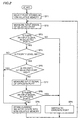
- Fig. 1 is a block diagram of an embodiment of the present invention.
- Fig. 2 is a flow chart for describing a specific operation of the embodiment of the present invention.
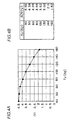
- Figs. 3A and 3B are diagrams indicating the relationship between a frequency of a horizontal synchronizing signal and a converted voltage value.
- Figs. 4A and 4B are diagrams showing the relationship between a frequency of a vertical synchronizing signal and a converted voltage value.
- a Dsub.B signal and a BNC.B signal, a Dsub.R signal and a BNC.R signal, a Dsub.G signal and a BNC.G signal, a Dsub.H signal and a BNC.H signal, and a Dsub.V signal and a BNC.V signal are applied to an analog switch 1.
- the synchronizing signals which can be used in the present invention, include a sync-on green signal having horizontal and vertical synchronizing signals added to a video signal G, a composite sync signal having a vertical synchronizing signal added to a horizontal synchronizing signal, and separate sync signals which are respectively independent horizontal and vertical synchronizing signals.
- Analog switch 1 responds to a switching signal 1 from a microcomputer 8 which will be described afterwards to switch between an input from BNC connectors and an input from a Dsub connector to separate an input signal into video signals R, G, B, and signals C.SYNC (Composite Sync), H.SYNC and V.SYNC. Signals C.SYNC, H.SYNC and V.SYNC are provided to a synchronizing processor 3.
- the Dsub connector includes fifteen, for example, input pins to which signals Dsub.B-Dsub.V are applied.
- Synchronizing processor 3 generates a horizontal drive signal HD and a vertical drive signal VD which are sent to a deflection system, and a horizontal synchronizing signal HS, a vertical synchronizing signal VS, and a synchronization information signal having the polarity arranged. Signals HS and VS and the synchronization information signal are applied to a synchronizing frequency detection circuit 4. Synchronizing frequency detection circuit 4 measures the frequencies of signals HS and VS to provide the frequency detecting signal to microcomputer 8.
- Signals Dsub.G and BNC.G, signals Dsub.H and BNC.H, and signals Dsub.V and BNC.V are also applied to an analog switch 2.
- Analog switch 2 responds to a switching signal 2 from microcomputer 8 to switch between the inputs from the BNC connector and the Dsub connector to generate and provide to a synchronizing processor 5 signals C'SYNC, H'SYNC and V'SYNC.
- Synchronizing processor 5 generates a horizontal synchronizing signal H'S and a vertical synchronizing signal V'S which are applied to F/V converters 6 and 7, respectively.
- F/V converters 6 and 7 set equal the respective pulse widths of signals H'S and V'S to integrate the pulses for conversion into a DC voltage.
- the DC voltage is applied to an A/D port of microcomputer 8.
- Microcomputer 8 determines change in the frequency according to a detection signal from synchronizing frequency detection circuit 4 and the voltage values applied from F/V converters 6 and 7.
- a switch 9 for setting the priority level and a non-volatile memory 10 for storing the current selected state of an input signal are connected to microcomputer 8. Switch 9 can be selectively set using on screen display.
- Microcomputer 8 provides switching signals 1 and 2 to select a port (input terminal) stored in non-volatile memory 10 at step (abbreviated as "SP" in the figure) SP1 of Fig. 2. It is assumed that analog switch 1 selects the Dsub connector end by switching signal 1, and analog switch 2 selects the BNC connector end by switching signal 2. Signal C.SYNC or signals H.SYNC and V.SYNC are generated according to a signal from the Dsub connector selected by analog switch 1 to be provided to synchronizing processor 3. Synchronizing processor 3 provides signals HD, VD, HS, VS, and a synchronization information signal according to an input synchronizing signal.
- Signals HS and VS and the synchronous information signal are applied to synchronizing frequency detection circuit 4.
- Microcomputer 8 causes synchronizing frequency detection circuit 4 to detect the synchronizing signal in response to the current selection of a signal from the Dsub connector at step SP2.
- a priority level is set for the Dsub connector at step SP4. It is determined that a priority level is set if switch 9 is closed.
- microcomputer 8 determines that a priority level is set, it is determined whether the priority level of the selected Dsub connector is high or not at step SP5. If the priority level is high, control proceeds to step SP6 where the currently selected information is stored in non-volatile memory 1. The operation of steps SP1-SP6 is executed repeatedly thereafter.
- step SP7 control proceeds to steps SP7 where the input signal of the BNC connector which is the opposite port is measured. More specifically, analog switch 2 selects a signal of the BNC connector end, which is applied to synchronizing processor 5.
- Signals H'S and V'S provided from synchronizing processor 5 are integrated by F/V converters 6 and 7.
- the relationship between the frequencies of signals H'S and V'S and the voltage value is as shown in Figs. 3A, 3B, 4A and 4B.
- Fig. 3A the frequency of a horizontal synchronizing signal corresponds to 20kHz-100kHz. Conversion of these frequencies into voltage values is shown in Fig. 3B. Referring to Fig.
- step SP8 the frequency of a vertical synchronizing signal corresponds to 40Hz-160Hz. Conversion of these frequencies into voltage values is shown in Fig. 4B.
- determination and switching of a signal can be effected instantaneously since the frequencies of synchronizing signals of two systems are continuously monitored. Unnecessary switching will not be carried out since the frequencies of the horizontal and vertical synchronizing signals can be measured. An intelligent control is possible since switching is not forced by means of hardware.
Landscapes
- Engineering & Computer Science (AREA)
- Physics & Mathematics (AREA)
- Computer Hardware Design (AREA)
- General Physics & Mathematics (AREA)
- Theoretical Computer Science (AREA)
- Controls And Circuits For Display Device (AREA)
- Electronic Switches (AREA)
Claims (10)
- Prioritätsschaltvorrichtungen zum Umschalten zwischen an mehrere Eingangsanschlüsse angelegten Eingangssignalen, mit:dadurch gekennzeichnet, dass die Umschalteinrichtung auf die Erkennung eines hohen Prioritätsniveaus reagiert, das für jeden der mehreren Eingangsanschlüsse auswählbar ist, um denjenigen Eingangsanschluss auszuwählen, für den das hohe Prioritätsniveau ausgewählt ist.einer Synchronisiersignal-Erkennungseinrichtung (4) zum Erkennen eines Synchronisiersignals, wenn ein solches im an die mehreren Eingangsanschlüsse angelegten Eingangssignal enthalten ist; undeiner Umschalteinrichtung (1, 2), die auf die Erkennung eines Synchronisiersignals durch die Synchronisiersignal-Erkennungseinrichtung reagiert, um denjenigen Eingangsanschluss, an den das Synchronisiersignal angelegt wird, auszuwählen und das an diesen Eingangsanschluss angelegte Eingangssignal zu liefern;
- Prioritätsschaltvorrichtungen nach Anspruch 1, ferner mit einer Prioritätsniveau-Einstelleinrichtung (9) zum Einstellen eines Prioritätsniveaus für die Eingangsanschlüsse.
- Prioritätsschaltvorrichtungen nach Anspruch 1 oder 2, ferner mit einem nichtflüchtigen Speicher zum Speichern von Information, die den Eingangsanschluss kennzeichnet, für den das Eingangssignal aktuell geliefert wird.
- Prioritätsschaltvorrichtungen nach Anspruch 1, 2 oder 3, bei der die Synchronisiersignal-Erkennungseinrichtung die Frequenz des Horizontal- und des Vertikal-Synchronisiersignals erkennt.
- Prioritätsschaltvorrichtungen nach einem der vorstehenden Ansprüche, bei der zu den Eingangsanschlüssen ein BNC-Verbinder und ein Dsub-Verbinder gehören.
- Verfahren zum Auswählen eines Eingangssignals eines Bilds, das auf einer Anzeigevorrichtung mit mehreren auswählbaren Signaleingabepfaden anzuzeigen ist, mit den folgenden Schritten:dadurch gekennzeichnet, dass das Verfahren Folgendes umfasst:Überwachen eines Eingangssignals auf einem zweiten Eingangssignalpfad während des Empfangs eines Eingangssignals auf einem aktuell ausgewählten ersten Eingangssignalpfad, um bei Erkennung desselben ein Umschaltsignal zu erzeugen; undAuswählen des zweiten Ausgangssignalpfads auf das Umschaltsignal hin;selektives Zuordnen eines Prioritätsniveaus zum ersten und zweiten Eingangssignalpfad, wobei der eine der Pfade ein hohes Prioritätsniveau aufweist;Erkennen, ob der erste oder der zweite Eingangssignalpfad das genannte hohe Prioritätsniveau aufweist; undAuswählen des zweiten Eingangssignalpfads auf das Umschaltsignal hin, wenn der zweite Eingangssignalpfad das hohe Prioritätsniveau aufweist, oder Beibehalten der aktuellen Auswahl des ersten Eingangssignalpfads, wenn dieser das hohe Prioritätsniveau aufweist.
- Verfahren nach Anspruch 6, ferner mit einem Einspeichern von Information, die den neu ausgewählten Eingangsanschluss kennzeichnet, in einem nichtflüchtigen Speicher.
- Verfahren nach Anspruch 7, bei dem jedes Eingangssignal ein Synchronisiersignal enthält, wobei es zum Erkennen, ob auf dem zweiten Eingangssignalpfad ein Eingangssignal vorhanden ist, das Erkennen gehört, ob auf dem zweiten Eingangssignalpfad ein Synchronisiersignal vorhanden ist.
- Verfahren nach Anspruch 7, bei dem das Synchronisiersignal ein Horizontal- und ein Vertikal-Synchronisiersignal enthält und bei dem zur Erkennung, ob ein Synchronisiersignal vorhanden ist, das Erkennen der Frequenz des Horizontalund des Vertikal-Synchronisiersignals gehört.
- Verfahren nach einem der Ansprüche 6 bis 9, bei dem der erste Eingangssignalpfad über einen BNC-Verbinder verfügt und der zweite Eingangssignalpfad über einen Dsub-Verbinder verfügt.
Applications Claiming Priority (3)
| Application Number | Priority Date | Filing Date | Title |
|---|---|---|---|
| JP22634195 | 1995-09-04 | ||
| JP226341/95 | 1995-09-04 | ||
| JP7226341A JPH0968958A (ja) | 1995-09-04 | 1995-09-04 | 入力信号の優先切換装置 |
Publications (2)
| Publication Number | Publication Date |
|---|---|
| EP0762378A1 EP0762378A1 (de) | 1997-03-12 |
| EP0762378B1 true EP0762378B1 (de) | 2001-11-14 |
Family
ID=16843657
Family Applications (1)
| Application Number | Title | Priority Date | Filing Date |
|---|---|---|---|
| EP96306396A Expired - Lifetime EP0762378B1 (de) | 1995-09-04 | 1996-09-04 | Eingangssignalschaltvorrichtung mit Priorität für Anzeigevorrichtung |
Country Status (4)
| Country | Link |
|---|---|
| US (1) | US5886545A (de) |
| EP (1) | EP0762378B1 (de) |
| JP (1) | JPH0968958A (de) |
| DE (1) | DE69616918T2 (de) |
Families Citing this family (16)
| Publication number | Priority date | Publication date | Assignee | Title |
|---|---|---|---|---|
| KR100214381B1 (ko) * | 1996-04-16 | 1999-08-02 | 구자홍 | 모니터의비엔씨(bnc),디서브(d-sub)신호자동절환회로 |
| KR100206114B1 (ko) * | 1996-10-11 | 1999-07-01 | 윤종용 | 외부 입출력 접속 적응형 비디오라인 접속장치 |
| US6122018A (en) * | 1997-01-17 | 2000-09-19 | Sony Corporation | Video display apparatus and method for controlling the switching of external input terminals thereof |
| KR100238579B1 (ko) * | 1997-04-15 | 2000-01-15 | 윤종용 | Dpms 기능을 갖는 디스플레이 장치의 bnc/d-sub 자동 선택 방법 및 장치 |
| US6559893B1 (en) * | 1998-01-02 | 2003-05-06 | Monster Cable Products, Inc. | Method and apparatus for automatic selection of video interface |
| JP3622481B2 (ja) * | 1998-03-13 | 2005-02-23 | 松下電器産業株式会社 | Av機器 |
| US6437834B1 (en) * | 1998-05-27 | 2002-08-20 | Nec Corporation | Video switching and mix/effecting equipment |
| TW516307B (en) * | 2000-03-17 | 2003-01-01 | Benq Corp | Display device with self-test circuit |
| US20020186329A1 (en) * | 2001-06-07 | 2002-12-12 | Ehometv [Hk] Ltd., | Electronic content modules and display dock |
| JP2003241724A (ja) * | 2002-02-15 | 2003-08-29 | Rohm Co Ltd | ディスプレイモニタ装置 |
| KR100449739B1 (ko) * | 2002-09-19 | 2004-09-22 | 삼성전자주식회사 | 디스플레이장치 및 디스플레이장치에 입력되는 신호의체크방법 |
| JP2007306117A (ja) * | 2006-05-09 | 2007-11-22 | Sharp Corp | 入力切替方法、入力切替装置、表示機器およびavシステム |
| KR20090094997A (ko) * | 2008-03-04 | 2009-09-09 | 삼성전자주식회사 | 모드 전환방법 및 이를 적용한 디스플레이 장치 |
| JP5625266B2 (ja) * | 2009-06-18 | 2014-11-19 | パナソニック株式会社 | 映像処理装置および映像表示装置 |
| JP5996929B2 (ja) * | 2012-05-08 | 2016-09-21 | Dxアンテナ株式会社 | 映像無線伝送装置 |
| CN103150134B (zh) * | 2013-03-26 | 2015-12-09 | 深圳市杰和科技发展有限公司 | 一种多屏幕显示切换系统及方法 |
Family Cites Families (10)
| Publication number | Priority date | Publication date | Assignee | Title |
|---|---|---|---|---|
| US4460918A (en) * | 1982-07-14 | 1984-07-17 | Zenith Electronics Corporation | Automatic switching circuit for a dual mode television receiver |
| US4682234A (en) * | 1985-12-31 | 1987-07-21 | North American Philips Consumer Electronics Corp. | Video noise reduction in picture-in-picture television receiver |
| US4665438A (en) * | 1986-01-03 | 1987-05-12 | North American Philips Corporation | Picture-in-picture color television receiver |
| JPH0715013Y2 (ja) * | 1987-06-25 | 1995-04-10 | 三菱電機株式会社 | カラ−デイスプレイ装置 |
| US5034818A (en) * | 1989-07-10 | 1991-07-23 | Samsung Electronics Co., Ltd. | Priority selector for external signals |
| US5202765A (en) * | 1991-05-06 | 1993-04-13 | Thomson Consumer Electronics, Inc. | Television receiver with picture in picture and non-linear processing |
| JPH0651729A (ja) * | 1992-06-05 | 1994-02-25 | Matsushita Electric Ind Co Ltd | 入力信号経路自動切り替え回路 |
| JPH0651730A (ja) * | 1992-06-05 | 1994-02-25 | Matsushita Electric Ind Co Ltd | 混合同期信号選択回路 |
| JP2921265B2 (ja) * | 1992-06-08 | 1999-07-19 | 松下電器産業株式会社 | テレビジョン受像機 |
| KR950005647B1 (ko) * | 1992-10-29 | 1995-05-27 | 주식회사금성사 | 엔티에스씨(ntsc) 신호와 에치디티브이(hdtv) 신호의 공용 수신시스템 |
-
1995
- 1995-09-04 JP JP7226341A patent/JPH0968958A/ja active Pending
-
1996
- 1996-09-03 US US08/711,394 patent/US5886545A/en not_active Expired - Lifetime
- 1996-09-04 DE DE69616918T patent/DE69616918T2/de not_active Expired - Lifetime
- 1996-09-04 EP EP96306396A patent/EP0762378B1/de not_active Expired - Lifetime
Also Published As
| Publication number | Publication date |
|---|---|
| DE69616918D1 (de) | 2001-12-20 |
| US5886545A (en) | 1999-03-23 |
| JPH0968958A (ja) | 1997-03-11 |
| DE69616918T2 (de) | 2002-04-11 |
| EP0762378A1 (de) | 1997-03-12 |
Similar Documents
| Publication | Publication Date | Title |
|---|---|---|
| EP0762378B1 (de) | Eingangssignalschaltvorrichtung mit Priorität für Anzeigevorrichtung | |
| US4821269A (en) | Diagnostic system for a digital signal processor | |
| KR100236505B1 (ko) | 비디오 시스템 | |
| US7009660B2 (en) | Device and method for automatically discriminating between formats of video signals | |
| EP1403844A2 (de) | Anzeigegerät mit Eingangssignalprüfung | |
| USRE40396E1 (en) | Method for detecting and separating vertical and horizonal synchronous signals from computer system | |
| US5764308A (en) | Method of adjusting hue and device therefor | |
| US20010055029A1 (en) | Display control apparatus and method | |
| US4954880A (en) | Color display apparatus | |
| US5757366A (en) | State indication circuit for a display system | |
| US5220423A (en) | Apparatus for controlling display of an image on a large aspect ratio television screen | |
| US5990971A (en) | Picture-display-region discriminating apparatus | |
| EP0283999B1 (de) | Farbbalkenselbstsucher | |
| US6384837B1 (en) | Symbol color compensating method for color display system | |
| US20050117059A1 (en) | Video-processing apparatus | |
| JP2897810B2 (ja) | 入力映像信号システム判別・切替え方式 | |
| US5343298A (en) | Correlation of a waveform to a video image | |
| EP0804024B1 (de) | Video-Zeilenformatwandler mit Benutzersteuerung | |
| KR20020082563A (ko) | 공용의 영상신호입력단을 구비한 영상재생장치 및 이를통한 영상재생방법 | |
| JP3128937B2 (ja) | 特殊効果装置 | |
| KR920000866Y1 (ko) | 입력신호 자동 선택회로 | |
| JPH06233203A (ja) | 表示装置及びテレビジョン受信機 | |
| US5760841A (en) | Apparatus for converting a video signal output from composite video instrument and method therefor | |
| KR100223206B1 (ko) | 영상신호 처리장치의 출력신호 선택방법 및 그 장치 | |
| KR100487319B1 (ko) | 티브이의 입력신호 처리장치 및 방법 |
Legal Events
| Date | Code | Title | Description |
|---|---|---|---|
| PUAI | Public reference made under article 153(3) epc to a published international application that has entered the european phase |
Free format text: ORIGINAL CODE: 0009012 |
|
| AK | Designated contracting states |
Kind code of ref document: A1 Designated state(s): CH DE FI FR GB IT LI NL SE |
|
| 17P | Request for examination filed |
Effective date: 19970417 |
|
| 17Q | First examination report despatched |
Effective date: 19980504 |
|
| GRAG | Despatch of communication of intention to grant |
Free format text: ORIGINAL CODE: EPIDOS AGRA |
|
| GRAG | Despatch of communication of intention to grant |
Free format text: ORIGINAL CODE: EPIDOS AGRA |
|
| GRAH | Despatch of communication of intention to grant a patent |
Free format text: ORIGINAL CODE: EPIDOS IGRA |
|
| GRAH | Despatch of communication of intention to grant a patent |
Free format text: ORIGINAL CODE: EPIDOS IGRA |
|
| GRAA | (expected) grant |
Free format text: ORIGINAL CODE: 0009210 |
|
| AK | Designated contracting states |
Kind code of ref document: B1 Designated state(s): CH DE FI FR GB IT LI NL SE |
|
| REG | Reference to a national code |
Ref country code: CH Ref legal event code: EP |
|
| REG | Reference to a national code |
Ref country code: CH Ref legal event code: NV Representative=s name: FREI PATENTANWALTSBUERO |
|
| REF | Corresponds to: |
Ref document number: 69616918 Country of ref document: DE Date of ref document: 20011220 |
|
| REG | Reference to a national code |
Ref country code: GB Ref legal event code: IF02 |
|
| ET | Fr: translation filed | ||
| PLBE | No opposition filed within time limit |
Free format text: ORIGINAL CODE: 0009261 |
|
| STAA | Information on the status of an ep patent application or granted ep patent |
Free format text: STATUS: NO OPPOSITION FILED WITHIN TIME LIMIT |
|
| 26N | No opposition filed | ||
| PGFP | Annual fee paid to national office [announced via postgrant information from national office to epo] |
Ref country code: FI Payment date: 20100910 Year of fee payment: 15 |
|
| PG25 | Lapsed in a contracting state [announced via postgrant information from national office to epo] |
Ref country code: FI Free format text: LAPSE BECAUSE OF NON-PAYMENT OF DUE FEES Effective date: 20110904 |
|
| REG | Reference to a national code |
Ref country code: FR Ref legal event code: PLFP Year of fee payment: 20 |
|
| PGFP | Annual fee paid to national office [announced via postgrant information from national office to epo] |
Ref country code: NL Payment date: 20150809 Year of fee payment: 20 |
|
| REG | Reference to a national code |
Ref country code: FR Ref legal event code: CD Owner name: EIZO CORPORATION, JP Effective date: 20150917 Ref country code: FR Ref legal event code: CA Effective date: 20150917 |
|
| PGFP | Annual fee paid to national office [announced via postgrant information from national office to epo] |
Ref country code: GB Payment date: 20150902 Year of fee payment: 20 Ref country code: DE Payment date: 20150902 Year of fee payment: 20 Ref country code: CH Payment date: 20150911 Year of fee payment: 20 |
|
| PGFP | Annual fee paid to national office [announced via postgrant information from national office to epo] |
Ref country code: SE Payment date: 20150911 Year of fee payment: 20 Ref country code: FR Payment date: 20150811 Year of fee payment: 20 |
|
| PGFP | Annual fee paid to national office [announced via postgrant information from national office to epo] |
Ref country code: IT Payment date: 20150925 Year of fee payment: 20 |
|
| REG | Reference to a national code |
Ref country code: DE Ref legal event code: R071 Ref document number: 69616918 Country of ref document: DE |
|
| REG | Reference to a national code |
Ref country code: NL Ref legal event code: MK Effective date: 20160903 |
|
| REG | Reference to a national code |
Ref country code: CH Ref legal event code: PL |
|
| REG | Reference to a national code |
Ref country code: GB Ref legal event code: PE20 Expiry date: 20160903 |
|
| PG25 | Lapsed in a contracting state [announced via postgrant information from national office to epo] |
Ref country code: GB Free format text: LAPSE BECAUSE OF EXPIRATION OF PROTECTION Effective date: 20160903 |
|
| REG | Reference to a national code |
Ref country code: SE Ref legal event code: EUG |