EP0756220B1 - Verbesserte Ladungspumpenschaltung - Google Patents
Verbesserte Ladungspumpenschaltung Download PDFInfo
- Publication number
- EP0756220B1 EP0756220B1 EP95830335A EP95830335A EP0756220B1 EP 0756220 B1 EP0756220 B1 EP 0756220B1 EP 95830335 A EP95830335 A EP 95830335A EP 95830335 A EP95830335 A EP 95830335A EP 0756220 B1 EP0756220 B1 EP 0756220B1
- Authority
- EP
- European Patent Office
- Prior art keywords
- charge
- node
- circuit
- transistor
- stage
- Prior art date
- Legal status (The legal status is an assumption and is not a legal conclusion. Google has not performed a legal analysis and makes no representation as to the accuracy of the status listed.)
- Expired - Lifetime
Links
Images

Classifications
-
- G—PHYSICS
- G05—CONTROLLING; REGULATING
- G05F—SYSTEMS FOR REGULATING ELECTRIC OR MAGNETIC VARIABLES
- G05F3/00—Non-retroactive systems for regulating electric variables by using an uncontrolled element, or an uncontrolled combination of elements, such element or such combination having self-regulating properties
- G05F3/02—Regulating voltage or current
- G05F3/08—Regulating voltage or current wherein the variable is dc
- G05F3/10—Regulating voltage or current wherein the variable is dc using uncontrolled devices with non-linear characteristics
- G05F3/16—Regulating voltage or current wherein the variable is dc using uncontrolled devices with non-linear characteristics being semiconductor devices
- G05F3/20—Regulating voltage or current wherein the variable is dc using uncontrolled devices with non-linear characteristics being semiconductor devices using diode- transistor combinations
- G05F3/24—Regulating voltage or current wherein the variable is dc using uncontrolled devices with non-linear characteristics being semiconductor devices using diode- transistor combinations wherein the transistors are of the field-effect type only
-
- H—ELECTRICITY
- H02—GENERATION; CONVERSION OR DISTRIBUTION OF ELECTRIC POWER
- H02M—APPARATUS FOR CONVERSION BETWEEN AC AND AC, BETWEEN AC AND DC, OR BETWEEN DC AND DC, AND FOR USE WITH MAINS OR SIMILAR POWER SUPPLY SYSTEMS; CONVERSION OF DC OR AC INPUT POWER INTO SURGE OUTPUT POWER; CONTROL OR REGULATION THEREOF
- H02M3/00—Conversion of dc power input into dc power output
- H02M3/02—Conversion of dc power input into dc power output without intermediate conversion into ac
- H02M3/04—Conversion of dc power input into dc power output without intermediate conversion into ac by static converters
- H02M3/06—Conversion of dc power input into dc power output without intermediate conversion into ac by static converters using resistors or capacitors, e.g. potential divider
- H02M3/07—Conversion of dc power input into dc power output without intermediate conversion into ac by static converters using resistors or capacitors, e.g. potential divider using capacitors charged and discharged alternately by semiconductor devices with control electrode, e.g. charge pumps
- H02M3/073—Charge pumps of the Schenkel-type
Definitions
- the present invention relates to a charge pump circuit with improved features.
- Charge pump circuits for generating a voltage of a given level (known as boost voltage) starting from a supply voltage that is at a lower level in order to supply a load arranged downstream of the charge pump circuit and requiring a supply voltage higher than the one directly available from the supply line, are known in the art.
- Charge pump circuits are based on the principle of alternating two separate steps: the first one includes charging a capacitor, and the second one includes raising the level of one terminal of the capacitor and connecting the other terminal to an output to achieve a voltage level that is higher than the power supply.
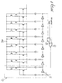
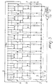
- figure 1 illustrates the complete charge pump circuit, constituted by a plurality of identical stages that are shown in detail in figure 2.
- Figure 1 thus shows the parallel connection of an odd number of voltage boost stages, designated by the reference numeral 2 i , between a power supply line 1 and a voltage boost line 9.
- Each stage shown in figure 2 comprises: a boost capacitor 3, in which the terminals form a first node 4 and a second node 5; an output diode 6, interposed between the second node 5 and the boost line 7; a charge transistor 8, interposed between the supply line 1 and the second node 5; a biasing diode 9, interposed between the supply line 1 and a node 10 formed by the gate terminal of the charge transistor 8; and an inverter 11, interposed between nodes 4 of two adjacent stages 2 i , except for the last stage, which is formed by a branch comprising an AND gate 12 followed by a NOR gate 13.
- the inverters 11 and the NOR circuit 13 constitute a loop oscillator with an odd number of inversion cycles.
- the above described charge pump circuit of the type known as "single-stage", has the purpose of raising the voltage on the boost line 7 to a value that is twice the supply voltage V DD minus a threshold value V T caused by the drop across the diodes 6; in other words, a voltage equal to 2V DD -V T is obtained.
- stage shown in figure 4 The difference between the stage shown in figure 4 and the stage of figure 2 resides in the presence of a first charge transfer diode 14 and of a second charge transfer diode 15.
- EP-A-0666571 for a detailed description of the pump circuit of figure 1 and of the pump circuit of figure 3.
- the voltage produced by the latter circuit is 3V DD -2V T .
- the principal aim of the present invention is therefore to provide a charge pump circuit that overcomes the drawbacks mentioned above, allowing to continuously achieve a high voltage level (boost voltage) in a short time and with maximum efficiency.
- an object of the present invention is to provide a charge pump circuit that allows to deliver maximum power during startup and in the initial step.
- Another object of the present invention is to provide a charge pump circuit that is more efficient from the point of view of overall impedance and therefore has a better current delivery capability.
- Another object of the present invention is to provide a charge pump circuit having a low capacitance with respect to known solutions.
- Another object of the present invention is to provide a charge pump circuit usable to drive large loads that require considerable current absorption.
- Another object of the present invention is to provide a charge pump circuit that is highly reliable and relatively easy to manufacture at competitive costs.
- a charge pump circuit that comprises a plurality of voltage boost stages that are mutually parallel-connected between a supply line and an output line, wherein each one of said stages comprises: first and second charge storage means in which, respectively, a first terminal is connected to a charge and discharge node and a second terminal is connected to a boost node to switch between a first charge step and a second step for transferring said charge to said output line; an inverter, in which an input node is connected to the boost node that is related to said first charge storage means and an output node is connected to the boost node that is related to said second charge storage means; a first charge transfer diode, which is connected between said charge and discharge node related to said first charge storage means and the charge and discharge node (29i) related to the second charge storage means (28i); a second charge transfer diode, which is connected between said charge and discharge node related to said second charge storage means and said output line; characterized in that each one of
- Figures 1-4 are diagrams of two known and previously described solutions of a charge pump circuit.
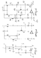
- the charge pump circuit according to the invention comprises a series of stages 20 1 , 20 2 ,... 20 n (where n is an odd number) that are mutually parallel-connected between a supply line 21 at the voltage V DD and an output line 22 (boost line); a loop oscillator, constituted by a plurality of mutually identical inverters 23 and by a flip-flop circuit 24, is connected to said output line.
- a capacitor 200 is connected to the boost line 22 and indicates the capacitive load to be driven by means of the charge pump circuit 100.
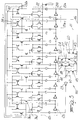
- stage 20 i The configuration of a stage 20 i is shown in detail in figure 6.
- the stage 20 i comprises first change storage means, advantageously constituted by a bootstrap capacitor 25 i , the terminals whereof constitute a first node 31 i and a second node 27 i .
- Each inverter 23 i is connected between an input node, which corresponds to the second node 27 i , and an output node 27 i+1 .
- the output node 27 i+1 coincides with the input node of the inverter 23 i+1 of a successive stage, whereas the input node 27 i coincides with the output node of the inverter 23 i-1 of a preceding stage.
- Second charge storage means which advantageously comprise a second capacitor 28 i , have a first terminal connected between the output node 27 i+1 and a second terminal forming a node 29 i .
- a first charge transfer diode 30 i is connected between the nodes 31 i and 29 i .
- a second charge transfer diode 32 i is connected between the node 40 i and the node 41 i on the boost line 22.
- the first diode 30 i and the second diode 32 i include native N-channel MOS transistors, that is to say, transistors having a low threshold and in which the drain and gate terminals are shorted together.
- a third biasing diode 33 i conveniently constituted by a native N-channel MOS transistor, has its drain terminal connected to the supply line 21 and its source terminal connected to the gate terminal of the first transistor 30 i .
- a fourth biasing diode 34 i advantageously constituted by a native N-channel MOS transistor, has its drain terminal connected to the supply line 21 and its source terminal connected to the circuit branch that includes the node 29 i , the capacitor 28 i , and the node 27 i+1 .
- the gate terminal of the transistor 32 i is connected to the above mentioned circuit branch and therefore to the source terminal of the transistor 34 i .
- the gate terminals of the transistors 33 i and 34 i are connected to each other and to the supply line 21.
- a fifth transistor 35 i is connected, by means of its gate terminal, to the circuit branch that connects the node 27 i to the node 31 i , forming a node 26 i .
- the source terminal of the transistor 35 i is connected to the boost line 22, whereas its drain terminal is connected to the source terminal of the transistor 33 i .
- the transistor 35 i is also advantageously provided as a native N-channel MOS transistor.
- a sixth transistor 36 i is connected to the supply line 21 by means of its drain terminal and to the supply line 21, at the voltage V DD , by means of its source terminal.
- a node 37 i is formed between the source terminal of the transistor 34 i and the node 29 i , and the gate terminal of a transistor 36 i+1 belonging to a successive stage 20 i+1 is connected to said node 37 i .
- the gate terminal of the transistor 36 i is connected to a node 37 i-1 belonging to a preceding stage 20 i-1 .
- Figure 5 shows the parallel connection of an odd number of stages 20 i and the connection of the last stage 20 n , in which the source terminal of the transistor 34 n is connected to the gate terminal of the transistor 36 2 of the second stage 20 2 .
- the source terminal of the transistor 34 n-1 belonging to the penultimate stage 20 n-1 is instead connected to the gate terminal of the transistor 36 1 belonging to the first stage 20 1 .
- the source terminal of the transistor 34 i of a generic stage 20 i is instead connected to the gate terminal of the transistor 36 i+2 of a stage 20 i+2 .
- the mutually connected gate terminals of the transistors 33 i and 34 i are connected, for each stage, to a control line 40 for enabling the pump circuit.
- Said line 40 allows to disconnect the transistors 33 i and 34 i from the power supply V DD if one wishes to leave the level of the boost line 22 unchanged, so as to then set the boost line to the ground level if required.
- the output node 27 i+1 of the penultimate stage 20 n-1 is connected, by means of a line 41, to the gate terminal of a transistor 43 belonging to a first pair of transistors 42 and 43 that are included in the flip-flop 24.
- the output node 27 i+1 of the last stage 20 n is instead connected, by means of a line 46, to the gate terminal of a transistor 45 belonging to a second pair of transistors 44 and 45.
- the gate terminal of the transistor 42 is connected to a line 60 for regulating the pump circuit 100 and the source terminal of said transistor is connected to the drain terminal of the transistor 43.
- the source terminal of the transistor 43 is connected to the ground and the drain terminal of the transistor 42 is connected to a node 47 of a latch circuit 50.
- Said flip-flop circuit 24 has the purpose of interrupting the operation of the charge pump circuit, freezing the last propagation that is occurring in the loop oscillator constituted by the inverters 23 i .
- the gate terminal of the transistor 44 is connected to the regulator line 60 of the pump circuit 100, the drain terminal of said transistor is connected to the source terminal of the transistor 44, and the source terminal is connected to the ground.
- the drain terminal of the transistor 44 is instead connected to a circuit branch connecting a second node 48 of the latch circuit 24 to the input node of an inverter 23, the output whereof is connected to the input node 27 1 of the first stage 20 1 of the charge pump circuit 100.
- the latch circuit comprises two pairs of MOS transistors.
- the first pair is formed by transistors 51 and 52, and the second pair is formed by transistors 53 and 54.
- the gate terminal of the transistor 53 is connected to the gate terminal of the transistor 54, and both gates are connected to the node 47.
- the gate terminal of the transistor 51 is connected to the gate terminal of the transistor 52, and both are connected to the node 48.
- the drain terminals of the transistors 51 and 53 are connected to the supply voltage V DD ; the source terminals of said transistors 51 and 53 are respectively connected to the drain terminals of the transistors 52 and 54; finally, the source terminals of the transistors 52 and 54 are connected to the ground.
- the capacitor 25 i begins to be precharged at the supply voltage V DD by means of the transistor 36 i , which has, from the preceding stage 27 i-1 , a voltage higher than V DD at its gate terminal, thus allowing the node 29 i to be connected to the supply V DD by means of the transistor 36 i . Then, when the node 27 i goes high, a further boosting by a voltage V DD occurs and the node 31 i reaches the level 2V DD .
- the capacitor 25 i could therefore transfer onto the boost line 22 a charge equal to 2V DD -V T , that is to say, a charge reduced by a threshold voltage V T of the transistor 35 i if the level of the line 22 is lower than 2V DD -V T .
- the capacitor 25 i discharges onto said boost line 22. Instead, when the level of the boost line approximates or equals the charge level 2V DD -V T , the charge of the node 31 i discharges onto the node 40 i (whose maximum possible level in this step is V DD ), which thus has the same charge as the node 29 i .
- the step for the discharge of the capacitor 25 i is followed by the step for precharging the capacitor 28 i when the nodes 27 i+1 go low.
- a voltage boost of one V DD is thus supplied to the node 29 i by means of the transistor 34 i .
- the node 29 i is thus charged at 3V DD -V T and discharges onto the boost line 22, minus a threshold V T determined by the transistor 32 i .
- the transfer of a charge equal to 3V DD -2V T onto the boost line has thus been achieved.
- the pump circuit behaves like a single-stage pump, transferring charge to the boost line 22.
- the level reached by said boost line is too high for further charge transfer to occur, that is to say, when a balance is reached, then it is not necessary to wait for discharge to continue transferring charges, but the second section of the stage 20 i of the pump circuit automatically becomes active and behaves, in this step, like a two-stage pump and is able to transfer charges to the boost line 22 by virtue of the higher voltage difference (3V DD -2V T ).
- This "two-stage” behavior thus engages after the “single-stage” behavior of the pump circuit in a gradual and progressive manner, until it becomes exclusively of the two-stage type only if the desired level is greater than, or equal to, 2V DD -V T .
- the output node of the inverter 23 n of the last stage 20 n has a low value (0), this value is transmitted over the line 46, is inverted by the two transistors 44 and 45, and is inverted again by the inverter 23; therefore, a high value (1) is present at the node 27 1 in the subsequent cycle.
- a 0 is present at the gate terminal of the transistor 43 and the transistors 42 and 43 are off. Instead, when a 1 is present on the line 41, the transistors 42 and 43 are on and the transistors 44 and 45 are off.
- the chart of figure 7 plots a comparison between the asymptotic value 2V DD -V T that can be attained with a single-stage pump (curve e) and the oscillating behavior of the nodes 27 i , 31 i , and 40 i , showing the asymptotic value that can be attained in theory by the pump according to the invention (curve d).
- the letter l designates the regular oscillation performed by the node 27 i which, starting from zero, reaches V DD at the most;
- the letter m designates the oscillation of the node 31 i , which starts from the level V DD and reaches at the most the level 2V DD ;
- the letter n designates the oscillation of the node 40 i .
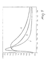
- Figure 8 is instead a chart that compares the voltage levels, as a function of time, obtainable with the pump configurations of the single-stage type, of the two-stage type, and according to the invention.
- the curve designated by (a) relates to the behavior of a single-stage pump, in which the attainable asymptotic voltage value is 2V DD -V T ;
- curve (b) relates to the behavior of a two-stage pump, in which the attainable asymptotic value is 3V DD -2V T ;
- curve (c) plots the voltage level that can be attained by a pump circuit according to the invention.
- curve (a) lies above curve (b) and practically coincides with curve (c); this shows that the single-stage pump is initially more efficient than the two-stage pump. Then, after a certain time, the behavior of curve (b) prevails and tends to reach a higher asymptotic level than curve (a).
- curve (c) is instead always higher than curves (a) and (b), although it then tends asymptotically towards the same value as curve (b).
- the pump circuit according to the invention behaves like a single-stage pump and then becomes a two-stage pump, but with an efficiency that is always higher than that of a conventional two-stage pump.
- Figure 9 is a chart that compares the current levels obtainable, as a function of time, by the two known types of charge pump circuit and by the circuit according to the invention.
- curve (f) relates to the current obtainable from a charge pump circuit of the "single-stage" type and therefore with high startup efficiency (high deliverable current) and with a sudden decrease in efficiency after a short period of time.
- Curve (h) shows the behavior of a "two-stage" charge pump circuit, with low initial efficiency due to the high impedance and with a later improvement (curve h passes above curve f).
- curve (g) plots the behavior of the circuit according to the invention, in which there is a high startup current value (equal to the curve f) and then there is a subsequent value that is in an intermediate position between curve (f) and curve (h).
- a regulator (not shown) is connected to the regulation line 60, so as to pump charges on the boost line, if required, and stop the charge pump circuit 100 when the desired voltage level is reached.
- the charge pump circuit according to the invention fully achieves the intended aim, since it allows to provide a voltage multiplier of the type with dual behavior, initially of the "single-stage” type, with an attainable asymptotic voltage level equal to 2V DD -V T , and then of the "two-stage” type, with an attainable asymptotic voltage level equal to 3V DD -2V T .
- This behavior of the charge pump circuit has the advantage that during the initial part, that is to say at startup, the circuit behaves like a single-stage pump, and therefore has a low impedance, allowing to quickly reach a relatively high voltage level. Then, when in theory the discharge step would end due to the rise in the voltage level of the boost line, the pump gradually becomes a two-stage pump, so as to therefore maintain good efficiency in a step in which the single-stage pump would be ineffective.
- an additional advantage of the pump circuit according to the invention is provided by the fact that the impedance remains constantly lower than in the single-stage solution and in the two-stage solution, allowing to deliver a higher current value than the single-stage case.
- the charge pump circuit according to the invention therefore allows to maintain the desired level, furthermore providing the ability to deliver current.
- the improved performance of the charge pump circuit allows to give smaller sizes and values to the capacitors of the circuit.
Landscapes
- Engineering & Computer Science (AREA)
- Microelectronics & Electronic Packaging (AREA)
- Physics & Mathematics (AREA)
- Power Engineering (AREA)
- Nonlinear Science (AREA)
- Electromagnetism (AREA)
- General Physics & Mathematics (AREA)
- Radar, Positioning & Navigation (AREA)
- Automation & Control Theory (AREA)
- Dc-Dc Converters (AREA)
Claims (14)
- Ladungspumpenschaltung (100), mit einer Vielzahl von Spannungserhöhungsstufen (20i), die gemeinsam parallel zwischen einer Versorgungsleitung (21) und einer Ausgabeleitung (22) verbunden sind, wobei jede der Stufen aufweist:erste (25i) und zweite (28i) Ladungsspeichermittel, in denen jeweils ein erster Anschluss mit einem Lade- und Entladeknoten (31i, 29i) und ein zweiter Anschluss mit einem Erhöhungsknoten (27i, 27i + 1) verbunden ist, um zwischen einem ersten Ladeschritt und einem zweiten Schritt zum Übertragen der Ladung auf die Ausgabeleitung (22) zu schalten, einen Inverter (23i), bei dem ein Eingangsknoten mit dem Erhöhungsknoten (27i), der dem ersten Ladungsspeichermittel (25i) zugeordnet ist, und ein Ausgabeknoten mit dem Erhöhungsknoten (27i + 1) verbunden ist, welcher dem zweiten Ladungsspeichermittel (28i) zugeordnet ist,eine erste Ladungstransferdiode (30i), die zwischen dem Lade- und Entladeknoten (31i), der dem ersten Ladungsspeichermittel (25i) zugeordnet ist, und dem Lade- und Entladeknoten (29i) verbunden ist, der dem zweiten Ladungsspeichermittel (28i) zugeordnet ist, eine zweite Ladungstransferdiode (32i), welche zwischen dem Lade- und Entladeknoten (29i), der dem zweiten Ladungsspeichermittel (28i) zugeordnet ist, und der Ausgabeleitung verbunden ist,dadurch gekennzeichnet, dass jede der Stufen (20i) eine zusätzliche Diode (35i) aufweist, die zwischen dem Lade- und Entladeknoten (31 i), der dem ersten Ladungsspeichermittel (25i) zugeordnet ist, und der Ausgabeleitung (22) verbunden ist,wobei die zusätzliche Diode (35i) das erste Ladungsspeichermittel (25i) entlädt, wenn das Potential der Ausgabeleitung (22) niedriger als das Potential des Lade- und Entladeknotens (31i), welcher dem ersten Ladungsspeichermittel (25i) zugeordnet ist, minus der Schwellenwertspannung der zusätzlichen Diode (35i) ist.
- Schaltung (100) nach Anspruch 1,
dadurch gekennzeichnet, dass sie eine dritte Vorspannungsdiode (33i) aufweist, die zwischen der Versorgungsleitung (21) und der ersten Ladungstransferdiode (30i) zwischengeschaltet ist. - Schaltung (100) nach Anspruch 1,
dadurch gekennzeichnet, dass sie eine vierte Vorspannungsdiode (34i) aufweist, die zwischen der Versorgungsleitung (21) und dem Lade- und Entladeknoten (29i) zwischengeschaltet ist, welcher dem zweiten Ladungsspeichermittel zugeordnet ist. - Schaltung (100) nach Anspruch 1,
dadurch gekennzeichnet, dass sie einen sechsten Transistor (36i) aufweist, welcher zwischen der Versorgungsleitung (21) und dem Lade- und Entladeknoten (31 i) verbunden ist, der dem ersten Ladungsspeichermittel (25i) zugeordnet ist, wobei der sechste Transistor ein N-Kanal MOS-Transistor mit niedrigem Schwellenwert ist. - Schaltung (100) nach Anspruch 1,
dadurch gekennzeichnet, dass die zusätzliche Diode (35i) einen N-Kanal MOS- Transistor mit niedrigem Schwellenwert aufweist, bei dem der Drain-Anschluss mit dem Source-Anschluss der dritten Vorspannungsdiode (33i) verbunden ist. - Schaltung nach Anspruch 1,
dadurch gekennzeichnet, dass die ersten, zweiten, dritten und vierten Dioden N-Kanal MOS-Transistoren mit niedrigem Schwellenwert aufweisen. - Schaltung nach den Ansprüchen 1, 2 und 3,
dadurch gekennzeichnet, dass die Gate-Anschlüsse der dritten und vierten Dioden mit einer Freigabesteuerleitung verbunden sind. - Schaltung nach den Ansprüchen 1, 3 und 4,
dadurch gekennzeichnet, dass der Source-Anschluss der vierten Diode einer gradzahligen Stufe in der Pumpenschaltung mit dem Gate-Anschluss des sechsten Transistors verbunden ist, welcher zu einer gradzahligen Stufe gehört. - Schaltung nach den Ansprüche 1, 3 und 4,
dadurch gekennzeichnet, dass der Source-Anschluss der vierten Diode einer ungradzahligen Stufe in der Pumpenschaltung mit dem Gate-Anschluss des sechsten Transistors verbunden ist, welcher ebenfalls zu einer ungradzahligen Stufe gehört. - Schaltung nach Anspruch 1,
dadurch gekennzeichnet, dass der Ausgabeknoten des Inverters der vorletzten Stufe der Pumpenschaltung mit dem Gate-Anschluss eines Transistors eines ersten Paares von Transistoren verbunden ist, wobei der Source-Anschluss des Transistors mit Masse verbunden ist, wobei der Gate-Anschluss des anderen Transistors des ersten Paares der Transistoren ein Signal zum Regulieren der Pumpenschaltung als Eingangssignal empfängt, wobei sein Drain-Anschluß mit einem ersten Knoten einer Latch-Schaltung verbunden ist. - Schaltung nach Anspruch 1 und 10,
dadurch gekennzeichnet, dass der Ausgabeknoten des Inverters der letzten Stufe der Pumpenschaltung mit dem Gate-Anschluss eines Transistors eines zweiten Paares von Transistoren verbunden ist, wobei der Source-Anschluss des Transistors mit Masse verbunden ist, wobei der Gate-Anschluss des anderen Transistors des zweiten Paares der Transistoren das Signal zur Regulierung der Pumpenschaltung als Eingangssignal empfängt, wobei sein Drain-Anschluss mit einem zweiten Knoten der Latch-Schaltung und einem Inverter verbunden ist, bei welchem der Ausgabeknoten mit dem Eingabeknoten des Inverters der ersten Stufe der Latch-Schaltung verbunden ist. - Schaltung nach Anspruch 10 und 11,
dadurch gekennzeichnet, dass das erste und zweite Paar von Transistoren und die Latch-Schaltung eine Flip-Flop-Schaltung bilden. - Schaltung nach Anspruch 1,
dadurch gekennzeichnet, dass das erste und zweite Ladungsspeichermittel jeweils einen Kondensator aufweist. - Schaltung nach einem oder mehreren der vorherigen Ansprüche,
dadurch gekennzeichnet, dass die Inverter und die Flip-Flop-Schaltung einen rückgekoppelten Oszillator mit einer ungradzahligen Anzahl von invertierenden Zyklen bilden.
Priority Applications (3)
| Application Number | Priority Date | Filing Date | Title |
|---|---|---|---|
| DE69519090T DE69519090T2 (de) | 1995-07-28 | 1995-07-28 | Verbesserte Ladungspumpenschaltung |
| EP95830335A EP0756220B1 (de) | 1995-07-28 | 1995-07-28 | Verbesserte Ladungspumpenschaltung |
| US08/684,192 US5760497A (en) | 1995-07-28 | 1996-07-19 | Charge pump circuit with multiple boost stages |
Applications Claiming Priority (1)
| Application Number | Priority Date | Filing Date | Title |
|---|---|---|---|
| EP95830335A EP0756220B1 (de) | 1995-07-28 | 1995-07-28 | Verbesserte Ladungspumpenschaltung |
Publications (2)
| Publication Number | Publication Date |
|---|---|
| EP0756220A1 EP0756220A1 (de) | 1997-01-29 |
| EP0756220B1 true EP0756220B1 (de) | 2000-10-11 |
Family
ID=8221982
Family Applications (1)
| Application Number | Title | Priority Date | Filing Date |
|---|---|---|---|
| EP95830335A Expired - Lifetime EP0756220B1 (de) | 1995-07-28 | 1995-07-28 | Verbesserte Ladungspumpenschaltung |
Country Status (3)
| Country | Link |
|---|---|
| US (1) | US5760497A (de) |
| EP (1) | EP0756220B1 (de) |
| DE (1) | DE69519090T2 (de) |
Families Citing this family (13)
| Publication number | Priority date | Publication date | Assignee | Title |
|---|---|---|---|---|
| US5801934A (en) * | 1996-12-12 | 1998-09-01 | Cypress Semiconductor Corp. | Charge pump with reduced power consumption |
| EP0856935B1 (de) * | 1997-02-03 | 2003-11-05 | Denso Corporation | Ladungspumpenschaltung |
| US5940876A (en) * | 1997-04-02 | 1999-08-17 | Advanced Micro Devices, Inc. | Stride instruction for fetching data separated by a stride amount |
| JPH11103254A (ja) * | 1997-09-26 | 1999-04-13 | Toshiba Corp | アナログデジタル変換回路装置及びその変換方法 |
| US5999425A (en) * | 1998-01-15 | 1999-12-07 | Cypress Semiconductor Corp. | Charge pump architecture for integrated circuit |
| US6208542B1 (en) | 1998-06-30 | 2001-03-27 | Sandisk Corporation | Techniques for storing digital data in an analog or multilevel memory |
| US6320797B1 (en) * | 1999-02-24 | 2001-11-20 | Micron Technology, Inc. | Method and circuit for regulating the output voltage from a charge pump circuit, and memory device using same |
| WO2000057557A1 (en) * | 1999-03-24 | 2000-09-28 | Arizona Digital, Inc. | Method and apparatus for boosting backplane drive circuits |
| US6430067B1 (en) * | 2001-04-12 | 2002-08-06 | Sun Microsystems, Inc. | Voltage multiplier for low voltage microprocessor |
| US6535446B2 (en) * | 2001-05-24 | 2003-03-18 | Ramtron International Corporation | Two stage low voltage ferroelectric boost circuit |
| KR100714034B1 (ko) * | 2003-10-10 | 2007-05-04 | 에스티마이크로일렉트로닉스 엔.브이. | 반도체 소자의 고전압 스위치 회로 |
| US7969235B2 (en) | 2008-06-09 | 2011-06-28 | Sandisk Corporation | Self-adaptive multi-stage charge pump |
| US9491151B2 (en) * | 2015-01-07 | 2016-11-08 | Ememory Technology Inc. | Memory apparatus, charge pump circuit and voltage pumping method thereof |
Family Cites Families (7)
| Publication number | Priority date | Publication date | Assignee | Title |
|---|---|---|---|---|
| US5036229A (en) * | 1989-07-18 | 1991-07-30 | Gazelle Microcircuits, Inc. | Low ripple bias voltage generator |
| GB2245112A (en) * | 1990-06-13 | 1991-12-18 | Philips Electronic Associated | Dc/dc voltage multiplier. |
| JPH07501679A (ja) * | 1991-10-30 | 1995-02-16 | ザイリンクス,インコーポレイテッド | ポンプ電圧発生器用レギュレータ |
| US5191232A (en) * | 1992-03-17 | 1993-03-02 | Silicon Storage Technology, Inc. | High frequency voltage multiplier for an electrically erasable and programmable memory device |
| US5301097A (en) * | 1992-06-10 | 1994-04-05 | Intel Corporation | Multi-staged charge-pump with staggered clock phases for providing high current capability |
| EP0666571B1 (de) * | 1994-01-28 | 2000-05-31 | STMicroelectronics S.r.l. | Ladungspumpenschaltung |
| US5532653A (en) * | 1995-02-07 | 1996-07-02 | National Semiconductor Corporation | Supply voltage compensated charge pump oscillator |
-
1995
- 1995-07-28 EP EP95830335A patent/EP0756220B1/de not_active Expired - Lifetime
- 1995-07-28 DE DE69519090T patent/DE69519090T2/de not_active Expired - Fee Related
-
1996
- 1996-07-19 US US08/684,192 patent/US5760497A/en not_active Expired - Lifetime
Also Published As
| Publication number | Publication date |
|---|---|
| DE69519090T2 (de) | 2001-06-13 |
| DE69519090D1 (de) | 2000-11-16 |
| EP0756220A1 (de) | 1997-01-29 |
| US5760497A (en) | 1998-06-02 |
Similar Documents
| Publication | Publication Date | Title |
|---|---|---|
| EP0756220B1 (de) | Verbesserte Ladungspumpenschaltung | |
| JP4865317B2 (ja) | 電荷ポンプ回路及び電荷ポンプ方法 | |
| TWI391805B (zh) | 廣大範圍供應電壓之有效率的充電泵 | |
| US6154088A (en) | Clocking scheme and charge transfer switch for increasing the efficiency of a charge pump or other circuit | |
| US6545529B2 (en) | High voltage generating circuit | |
| US7855591B2 (en) | Method and system for providing a charge pump very low voltage applications | |
| US5519360A (en) | Ring oscillator enable circuit with immediate shutdown | |
| US6828849B2 (en) | Voltage generating/transferring circuit | |
| US5650671A (en) | Charge pump circuit | |
| US20050093614A1 (en) | Multi stage voltage pump circuit | |
| US7176746B1 (en) | Low power charge pump method and apparatus | |
| US5493486A (en) | High efficiency compact low power voltage doubler circuit | |
| KR100300077B1 (ko) | 가변 오실레이션 주기를 갖는 차지펌프회로 | |
| US20080143401A1 (en) | Charge pump circuit | |
| US5412257A (en) | High efficiency N-channel charge pump having a primary pump and a non-cascaded secondary pump | |
| US5502415A (en) | Booster power generating circuit | |
| US20070090871A1 (en) | High voltage generation circuit and semiconductor device having the same | |
| KR101295777B1 (ko) | 차지 펌핑 회로 | |
| US7714636B2 (en) | Charge pump circuit and cell thereof | |
| JPH0740437B2 (ja) | 遅延回路 | |
| KR100478866B1 (ko) | 저전력발진기 | |
| US7847617B2 (en) | Charge pump and method for operating the same | |
| US20050077951A1 (en) | High voltage switch circuit of semiconductor device | |
| JPH06343260A (ja) | チャージポンプ回路 | |
| GB2035629A (en) | Regulated high voltage power supply |
Legal Events
| Date | Code | Title | Description |
|---|---|---|---|
| PUAI | Public reference made under article 153(3) epc to a published international application that has entered the european phase |
Free format text: ORIGINAL CODE: 0009012 |
|
| AK | Designated contracting states |
Kind code of ref document: A1 Designated state(s): DE FR GB IT |
|
| 17P | Request for examination filed |
Effective date: 19970626 |
|
| RAP3 | Party data changed (applicant data changed or rights of an application transferred) |
Owner name: STMICROELECTRONICS S.R.L. |
|
| GRAG | Despatch of communication of intention to grant |
Free format text: ORIGINAL CODE: EPIDOS AGRA |
|
| 17Q | First examination report despatched |
Effective date: 19991018 |
|
| GRAG | Despatch of communication of intention to grant |
Free format text: ORIGINAL CODE: EPIDOS AGRA |
|
| GRAG | Despatch of communication of intention to grant |
Free format text: ORIGINAL CODE: EPIDOS AGRA |
|
| GRAH | Despatch of communication of intention to grant a patent |
Free format text: ORIGINAL CODE: EPIDOS IGRA |
|
| GRAH | Despatch of communication of intention to grant a patent |
Free format text: ORIGINAL CODE: EPIDOS IGRA |
|
| GRAA | (expected) grant |
Free format text: ORIGINAL CODE: 0009210 |
|
| AK | Designated contracting states |
Kind code of ref document: B1 Designated state(s): DE FR GB IT |
|
| REF | Corresponds to: |
Ref document number: 69519090 Country of ref document: DE Date of ref document: 20001116 |
|
| ITF | It: translation for a ep patent filed |
Owner name: MODIANO & ASSOCIATI S.R.L. |
|
| ET | Fr: translation filed | ||
| PLBE | No opposition filed within time limit |
Free format text: ORIGINAL CODE: 0009261 |
|
| STAA | Information on the status of an ep patent application or granted ep patent |
Free format text: STATUS: NO OPPOSITION FILED WITHIN TIME LIMIT |
|
| 26N | No opposition filed | ||
| REG | Reference to a national code |
Ref country code: GB Ref legal event code: IF02 |
|
| PGFP | Annual fee paid to national office [announced via postgrant information from national office to epo] |
Ref country code: DE Payment date: 20040806 Year of fee payment: 10 |
|
| PG25 | Lapsed in a contracting state [announced via postgrant information from national office to epo] |
Ref country code: IT Free format text: LAPSE BECAUSE OF NON-PAYMENT OF DUE FEES;WARNING: LAPSES OF ITALIAN PATENTS WITH EFFECTIVE DATE BEFORE 2007 MAY HAVE OCCURRED AT ANY TIME BEFORE 2007. THE CORRECT EFFECTIVE DATE MAY BE DIFFERENT FROM THE ONE RECORDED. Effective date: 20050728 |
|
| PG25 | Lapsed in a contracting state [announced via postgrant information from national office to epo] |
Ref country code: DE Free format text: LAPSE BECAUSE OF NON-PAYMENT OF DUE FEES Effective date: 20060201 |
|
| PGFP | Annual fee paid to national office [announced via postgrant information from national office to epo] |
Ref country code: GB Payment date: 20060627 Year of fee payment: 12 |
|
| PGFP | Annual fee paid to national office [announced via postgrant information from national office to epo] |
Ref country code: FR Payment date: 20060728 Year of fee payment: 12 |
|
| GBPC | Gb: european patent ceased through non-payment of renewal fee |
Effective date: 20070728 |
|
| PG25 | Lapsed in a contracting state [announced via postgrant information from national office to epo] |
Ref country code: GB Free format text: LAPSE BECAUSE OF NON-PAYMENT OF DUE FEES Effective date: 20070728 |
|
| REG | Reference to a national code |
Ref country code: FR Ref legal event code: ST Effective date: 20080331 |
|
| PG25 | Lapsed in a contracting state [announced via postgrant information from national office to epo] |
Ref country code: FR Free format text: LAPSE BECAUSE OF NON-PAYMENT OF DUE FEES Effective date: 20070731 |