EP0755618B1 - Sealed electronic packaging for environmental protection of active electronics - Google Patents
Sealed electronic packaging for environmental protection of active electronics Download PDFInfo
- Publication number
- EP0755618B1 EP0755618B1 EP95916228A EP95916228A EP0755618B1 EP 0755618 B1 EP0755618 B1 EP 0755618B1 EP 95916228 A EP95916228 A EP 95916228A EP 95916228 A EP95916228 A EP 95916228A EP 0755618 B1 EP0755618 B1 EP 0755618B1
- Authority
- EP
- European Patent Office
- Prior art keywords
- sealed
- electronics
- packaging
- active electronics
- connector
- Prior art date
- Legal status (The legal status is an assumption and is not a legal conclusion. Google has not performed a legal analysis and makes no representation as to the accuracy of the status listed.)
- Expired - Lifetime
Links
Images


Classifications
-
- H—ELECTRICITY
- H05—ELECTRIC TECHNIQUES NOT OTHERWISE PROVIDED FOR
- H05K—PRINTED CIRCUITS; CASINGS OR CONSTRUCTIONAL DETAILS OF ELECTRIC APPARATUS; MANUFACTURE OF ASSEMBLAGES OF ELECTRICAL COMPONENTS
- H05K5/00—Casings, cabinets or drawers for electric apparatus
- H05K5/06—Hermetically-sealed casings
- H05K5/068—Hermetically-sealed casings having a pressure compensation device, e.g. membrane
-
- H—ELECTRICITY
- H05—ELECTRIC TECHNIQUES NOT OTHERWISE PROVIDED FOR
- H05K—PRINTED CIRCUITS; CASINGS OR CONSTRUCTIONAL DETAILS OF ELECTRIC APPARATUS; MANUFACTURE OF ASSEMBLAGES OF ELECTRICAL COMPONENTS
- H05K5/00—Casings, cabinets or drawers for electric apparatus
- H05K5/0026—Casings, cabinets or drawers for electric apparatus provided with connectors and printed circuit boards [PCB], e.g. automotive electronic control units
- H05K5/003—Casings, cabinets or drawers for electric apparatus provided with connectors and printed circuit boards [PCB], e.g. automotive electronic control units having an integrally preformed housing
-
- H—ELECTRICITY
- H05—ELECTRIC TECHNIQUES NOT OTHERWISE PROVIDED FOR
- H05K—PRINTED CIRCUITS; CASINGS OR CONSTRUCTIONAL DETAILS OF ELECTRIC APPARATUS; MANUFACTURE OF ASSEMBLAGES OF ELECTRICAL COMPONENTS
- H05K5/00—Casings, cabinets or drawers for electric apparatus
- H05K5/0026—Casings, cabinets or drawers for electric apparatus provided with connectors and printed circuit boards [PCB], e.g. automotive electronic control units
- H05K5/0039—Casings, cabinets or drawers for electric apparatus provided with connectors and printed circuit boards [PCB], e.g. automotive electronic control units having a tubular housing wherein the PCB is inserted longitudinally
-
- H—ELECTRICITY
- H05—ELECTRIC TECHNIQUES NOT OTHERWISE PROVIDED FOR
- H05K—PRINTED CIRCUITS; CASINGS OR CONSTRUCTIONAL DETAILS OF ELECTRIC APPARATUS; MANUFACTURE OF ASSEMBLAGES OF ELECTRICAL COMPONENTS
- H05K3/00—Apparatus or processes for manufacturing printed circuits
- H05K3/22—Secondary treatment of printed circuits
- H05K3/28—Applying non-metallic protective coatings
- H05K3/284—Applying non-metallic protective coatings for encapsulating mounted components
Definitions
- This invention relates to environmental protection for active electronics. More specifically, this invention relates to sealed electronics packaging for the environmental protection of active electronic circuit boards and the like assemblies. In particular, this invention relates to environmental packaging which permits access to the active electronics boards for repair and reconstruction.
- the typical small remote electronics unit deployed in the telephone network will be installed by technicians with few tools and limited supervision.
- the service life of these electronics is expected to be 20 years. Because these units will be relatively expensive, it is also important that they be repairable during production and later when retrieved from the field.
- These systems will also require a full range of component types to deliver the high performance/cost ratio required by the new network architectures.
- the active electronics device such as assemblies of microprocessors, dynamic random access memory (DRAMS) and/or other components such as resistors, capacitors, transformers, circuit protection devices, electro-optical devices and the like
- DRAMS dynamic random access memory
- other components such as resistors, capacitors, transformers, circuit protection devices, electro-optical devices and the like
- This is generally been approached through sealing the components in a conductive plastic tube or transparent or semi-transparent plastic or nickel coated plastic type bag (see e.g. US-A-5 005 106).
- US-A-5 005 106 see e.g. US-A-5 005 106.
- the invention pertains to the environmental sealing of active electronics by means of an environmentally protecting flexible packaging material including a moisture barrier therein combined with a sealed connector system which protects the electronics even during the heat generating active operations made without overheating the electronics.
- the sealing system has no impact on the electronics assembly process and may be removed and replaced many times without damaging the electronics allowing full repair of the electronics.
- the use of plastic materials in the seals and packaging produces a non-hermetic package; the potential harmful effects of moisture and other harmful chemicals which can diffuse through the plastic materials can be absorbed by optionally including a small amount of desiccant/absorbent inside the package.
- the invention provides protection apparatus for an active electronics circuit board, comprising:
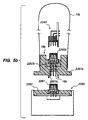
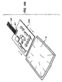
- Figure 1 illustrates the sealed electronics packaging 100 of a shape capable of accepting a complete active electronics board 1000.
- the sealed electronic packaging can have any suitable shape capable of accepting the desired shaped electronics board.
- the packaging can be made of separate sheets bonded together or a single sheet folded over as illustrated.
- the sealed electronics packaging 100 includes a sheet 10 of an environmentally protecting moisture insensitive material formed into a tube that is sized to accept an active electronics board 1000.
- the tube can be made with either a lap or fin seal.
- the sheet material 10 is sealed either with an adhesive or fused along a longitudinal seam 12 and around an adapter module 18 with pin contacts 16 passing through the adapter and protruding on the inside and outside of the adapter module.
- a gas tight seal is constructed around of the pin contacts 16 as they pass through the adapter 18 in a manner described below.
- the pin contacts 16 protruding on the inside of packaging 100 are capable of mating with the connector 19 on the electronics board 23 and the pin contacts 16 protruding on the outside of the packaging 100 are capable of mating with a sealed connector 20 which carries the signals from the active electronics 1000 to the rest of the system.
- Stabilizer blocks 25 are attached to the active electronics 1000 to prevent damage to the electronics. This feature will be described in greater detail below.
- the active electronics 1000 are inserted into the open end of the illustrated packaging 100 until the connector 19 plugs into the connector pins 16 protruding on the inside of packaging 100. In some cases the active electronics 1000 will have sharp points extending a short distance from it's surfaces.
- this seal could be made using a gel type sealant and a metal clip, velcro, or extruded zipper. These types of seals have the advantage that they can easily be opened and reclosed.
- a one way valve can be included into the bag to out-gas excess pressure if the bag were sealed at sea level and then moved to a high altitude application or preferably slack volume can be introduced during final sealing so that with temperature or pressure changes during operations, the volume of the flexible laminate barrier can change without generating internal pressure.
- a suitable temperature operating range is from about -40°C (-40°F) to about 93.3°C (200°F).
- the pressure will vary from a water head of about 6.1 m (20 feet) to an effective altitude of about 6096 m (20,000 feet).
- the layers of material 10 and particularly the preferred embodiments are described in Figure 2, and generally must resist the ingress of moisture resist puncture by any sharp protrusion and maintain its integrity for the life of the product.
- Any laminate or substrate material capable of resisting puncture, withstanding chemical environments, and temperature extremes while maintaining a high level of protection against moisture ingress and other environmental hazards and the like is suitable for use in this invention.
- materials which are known to be stable and consistent over time in these environments are suitable.
- a preferred laminate construction would be of sufficient thickness to be handled without puncture, tear or loss of seal integrity. Ranges for the layer thickness are up to 3.0 x 10 -4 m (12 mils) for the outside layers, 1.0 x 10 -4 m (4 mils) for the inside layers, and 2.5 x 10 -5 m (1 mil) for the middle layer.
- a particular sheet material 10 comprises top and bottom layers of a suitable material such as high density polyethylene about 1.5 x 10 -4 m (6 mils) thick and interior layers of ionomer about 5.0 x 10 -5 m (2 mils) thick and a center layer 2.5 x 10 -5 m (1 mil) of a metal such as aluminum or other suitable material.
- Interlaminar bond strength should remain above 35.7 kg/m (2 lbs./inch) as per ASTM D 1876 -93.
- the interior surface of the material may be made black to absorb heat radiated by the active electronics during operation.
- the exterior and or the interior surfaces may be made with an antistatic coating to reduce electro-static-discharge ESD potential.
- the envelope is an inner and an outer layer of plastic with a central metal layer. Suitable thicknesses are 3.8 x 10 -4 m (15 mls.), 2.5 x 10 -5 m (1 mls.) and 3.8 x 10 -4 m (15 mls.), respectively.
- the puncture resistance of the material when tested using ASTM F 1306 - 90 with a screwdriver type tip should be greater than 11.3 kg (25 lbs.), and with a pin type tip should be greater than 6.8 kg (15 lbs).
- the screwdriver puncture resistance should be greater than 13.6 kg (30 lbs) and pin resistance 9.1 kg (20 lbs).
- the material should have a tear resistance of greater than 3.6 kg (8 lbs), preferably greater than 5.4 kg (12 lbs.) when tested according to ASTM D 2582 -93.
- the heat seal obtained at the seams of the laminate when formed into a pouch should resist separation by a force of greater than 13.6 kg (30 lbs.) most preferably greater than 15.9 kg (35 lbs.) when tested to ASTM D 1876 -93. These performance characteristics should not degrade significantly with time or environmental exposure.
- FIG. 1 A suitable laminate is illustrated in PCT application WO 92/19034, (US Serial No. 08/129,201, filed October 13, 1993) completely incorporated herein by reference for all purposes but any laminate layer capable of resisting puncturing while providing inhibition to moisture ingress and protection from environmental hazards such as pollution and the like is suitable for use in the invention.
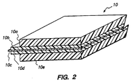
- Figure 2 illustrates a preferred laminate construction.
- Ranges for the layers can be between about 75 and 350 microns for layers 10a and 10e between about 20 to 200 microns for layers 10b and 10d, and between about 5 to 75 microns for layer 10c.
- the particular sheet material 10 comprises top and bottom layers 10a and 10e of a suitable material such as low density polyethylene about 200 microns (8 mls thick) and two interior layers about 80 microns (3 mls thick) of cast polyamide or polyester and a central layer of about 20 microns (1 ml thick) of aluminum or other suitable material.
- the interior of surface of the material may include a black paint or other material to absorb heat radiated by the active electronics during operation. By interior it is meant that portion of the sheet which upon welding into an envelope or an enclosure will have the black sides facing each other on opposite sides of the electronics board.
- the laminate have a three dimensional shape rather than be flat. This can be achieved by forming the sheet before welding. If a large volume enclosure is required, the aluminum layer could be replaced with a highly plastic metal such as commonly found in tin, tin alloys, and the like to sustain large deformations.
- the material used to make window 21 must also, as much as possible, block the transmission of moisture, chemical pollutants, and electronic noise while remaining transparent. This can be accomplished by using transparent plastics coated with thin coatings of inorganic materials such as indium tin oxide (ITO), Si0 2 , doped TiO 2 , doped AL 2 0 3 , and the like..
- ITO indium tin oxide
- Si0 2 Si0 2
- doped TiO 2 doped Al 2 0 3
- a multilayer laminate made of polyester and low density polyethylene can be used with or without the inorganic coating.
- the sheet material 10 can be fused to the adapter 18 if the inner layer of the flexible laminate and the adapter are made out of similar polymer materials. Fusion is the preferred approach. For example, making the adapter out or polyethylene or a suitable thermoplastic material common to both packaging and injection molding, and making the inner layer of the sheet material also of the same material, by applying sufficient heat to the area the materials will fuse together. Additionally, having the outer layer of the material match the adapter material would allow the outer layer to flow and bond with the adapter material, covering the raw edge of the sheet material.
- the edges can be adhesively sealed to form the closure.
- the sheet material 10 is sealed to the adapter 18 by means of a hot melt adhesive or a reactive hot melt adhesive.
- a hot melt adhesive e.g. a styrene-butadiene-styrene, SBS polyamide or polyester based hot melt adhesive or thermosetting epoxy, polyurethane or polyester could be used.
- the foil layer in the sheet material 10 may be effective for this purpose, and a conductive layer can be deposited on the inner surfaces of the adapter 18 by a variety of processes such as vapor deposition, plating, or painting with conductive paint. Care must be taken to avoid shorting out the connector pins 16.
- an electrically conductive hot melt adhesive may be used.
- Electrically conductive hot melts can be formulated by the addition of conductive fillers to standard hot melt adhesives. Descriptions of such materials and also alternatively ferromagnetic fillers could be used so that an alternating magnetic field will provide the heating during assembly. Raychem's US patent application 08/049,900 describes such materials. The application is completely incorporated herein by reference for all purposes.
- a desiccant/scavenger packet 22 addresses this transmission issue where it poses a problem.
- the package absorbs this small quantity of moisture and pollutants over the 20 year life of the system.
- silica gel, alumina, and molecular sieves are used to absorb moisture and polluting gases.
- the packet 22 is anchored inside the packaging 100 such that the clear view through the window 21 is retained.
- the desiccant/scavenger material is sealed in a polyethylene bag with a moisture vapor transmission rate sufficiently high to keep the relative humidity low inside the sealed electronic package but low enough to protect the desiccant from the humidity before the electronic package is sealed.
- the desiccant/scavenger material is sealed in an impermeable package that has a hole punched on one side. This hole is sealed by an adhesive patch attached to a long colored ribbon. Using a pressure sensitive adhesive, the pack is attached in a convenient location inside the packaging 100 with the ribbon passing out of the open end and with its free end attached to the outside of the packaging 100.
- the assembler Before the final sealing of the back edge 14 can be done the assembler must pull out the ribbon thus exposing the desiccant/scavenger at the last moment before the final seal is made. After this final seal is made, the seal integrity can be tested by heating the sealed electronics packaging 100 in an oven for a few minutes or hours. The heat will cause the air in the packaging 100 to expand and leak out or visibly expand the package envelope of a properly sealed unit. When the units are returned to room temperature the leaking ones will collapse and be readily detected.
- a pressure test can be performed by inserting a rubber stopper into the open end of the package with air pressure connected through the stopper and lowering the system into water. By pressurizing the package underwater any leakage will be visible as air bubbles.
- a further alternative test is a vacuum or a squeeze test which can be used for the same purpose.
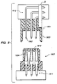
- FIG. 3 illustrates the cross-sectional view of a commonly available sealed connector. It consists of a male pin half 1900; a sealing gasket 1901; connector pins 1902; a female half 1903; and connector receptacles 1904.
- the male half 1900 is mated with the female half 1903 the sealing gasket 1901 is pressed tightly against the connector housing top 1910 making a seal.
- the connector backsides 1911 and 1912 are sealed by potting material or by the packaging 100, then water cannot leak into the cavity around the connector receptacles 1904.
- This type of connector design will prevent the formation of conductive paths within the connector for a short period of time, but because moisture and pollutants can transmit through the molded plastic polymer holding the pins, if continuously exposed to high humidity and pollution, the cavity surrounding the receptacles 1904 will eventually become wet and contaminated. This contamination will provide leakage paths between the pin connector receptacles 1904 and corrosion of the pin receptacles 1904 and the pins 1902 will take place, degrading the quality of the connection.
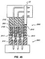
- Figure 4 and 4b a show a partial cross-sectional view of the connector of the preferred embodiment that provides a greatly improved sealed connector.
- the male half 2000 is identical to the conventional male half 1900 but the construction of the female half 2003 differs from the female half 1903.
- the female half 2003 is fabricated by inserting the receptacles 2004 into a polymer base plate 2016. Then a polymer upper cover 2015 is installed over the receptacles 2004.
- the upper cover 2015 is molded with baffles 2013 that surround each receptacle 2004 and extend almost to the base plate 2016.
- a hydrophobic sealant material such as a grease or preferably an elastic gel is added into the female half 2003 to almost completely fill the cavity in the female half 2003.
- Silicone gels as described in patents 5,111,497; 5,246,383; Serial No. 07/006,917, completely incorporated herein by reference for all purposes, are particularly suitable for this purpose because the gels will adhere to the surfaces inside the connector and yet are sufficiently elastic that the gels will not interfere with the deflection of the receptacle during insertion of the pin contact 2012. These gels are extremely effective at keeping water off of metal and plastic contact surfaces. Preferred gels include the property of being hydrophobic.
- the DIN connector series (Per DIN 41612, IEC 603-2) manufactured by T&B and other manufactures contain baffles which prevent the accidental contact of the receptacles 2004 and to support small wedges that hold the elastic arms of the receptacles 2004 in a pre stressed state beneficial to making a good contact. These structures are serendipitously useful for the purpose of sealing.
- An additional surprising benefit of a silicone gel material is that its extremely low surface energy causes it to wet to surfaces aggressively.
- the large surface area produced by the internal baffles 2013 makes it possible to fill the connector cavity by simply pouring the uncured gel through the small holes in the housing top 2010. The low surface energy allows the liquid to creep through the holes, coat the walls of each interior surface and fill the connector completely.
- a viscosity of less than 1.0 Nsm -2 (1000 centipoise), preferably about 0.8 Nsm -2 (600 centipoise), for the uncured gel is sufficiently low to permit filling a connector with a distance between pins of about 25.4 cm (10 inches).
- the presence of gel or grease in the female half 2003, particularly at the bottom where the polymer base plate 2016 meets polymer upper cover 2015 and the baffle 2013 will prevent the formation of a moisture and contaminant track between the receptacles 2004.
- This gel or grease should be sufficiently soft to allow encapsulation of the mating pins in the male half 2000 without excessive force.
- a hardness in the range of 15-50 grams as measured by a texture analyzer using standard MQC procedures will satisfy these conditions.
- Patent 4,852,636 completely incorporated herein by reference for all purposes, teaches a procedure known to the ordinary artisan for determining gram hardness of a material. This is sometimes referred to as Voland hardness.
- the gasket 2001 in the male half 2000 could be made of rubber or gel material with a higher elastic modules and hardness. A hardness in the range of 30-70 grams will satisfy the requirement that the gel or rubber in the male half must withstand multiple reentries without damage to the gel sufficient to cause it to lose its sealing capability.
- a gel with a hardness of 30-50 grams will satisfy the requirements of both the female half 2003 and the male half 2000 and could be used interchangeably in both areas.
- the gel material has the advantage that it will readily break up moisture tracks on the housing top 2010 because of the hydrophobic properties of the gel material. Thus the connector could be mated with moisture present on the surfaces and a high insulation resistance could be achieved.
- the gel type gasket is preferably be cured in place to achieve a high adhesion with the male half 2000.
- this gel type gasket could be fabricated by punching out an open cell foam reinforced gel sheet as described in detail in US Patent 4,865,905 and US Serial No. 07/762,533 filed January 14, 1992, said patent and application are completely incorporated herein by reference for all purposes.
- These gaskets can be retained in place by molding gripping features into the adapter 18 (Fig. 1) or by means of a mechanical frame that snaps or screws into place.
- Figure 4b illustrates another advantage of this design.
- the mechanical stress in the gel is high only on the material near the top of the cavity in the female half 2003 so loss of gel and the production of voids 2100 that can become moist tends to be only in this area.
- These voids are isolated from each other by the gel sealing the lower path 2101 between the receptacles at the bottom of the female half 2003 and by the gel or rubber gasket 2001 pressed on the housing top 2010 that blocks the upper path 2102.
- a coaxial connector will be used to interconnect high frequency signals into the active electronics 1000.
- the same sealing technique can be used with this type of connector where the center female contact is filled with gel to prevent shorting leaks from the center contact to the ground.
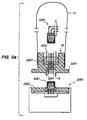
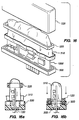
- Figures 5a and 5b illustrates a cross-sectional view of the adapter 18 or 18b installed in an injection molded part 2201 or 2201b (18 in Fig. 1) and sealed using a potting material 2203 or 2203b such as a 2 part curable polyurethane or epoxy compound.
- Figure 5e is the male-female embodiment while Figure 5b is the female-male embodiment.
- the main difference is socket 2250 in Figure 5a and the pin embodiment 2240 in Figure 5b.
- Identical parts are labeled the same while alternative embodiments include "b" next to the number in Figure 5b.
- the flexible sealing bag 10 is bonded to the molded part.
- a close fitting plug can be inserted in place of the gasket 2001 until the potting material cures.
- Figure 6 illustrates a alternative adapter design where the contact pins 16 are inserted or molded directly into the molded adapter part 2211.
- the sealing bag 10 is subsequently attached.
- This embodiment saves the potting step and in essence creates a one part DIN connector interface between the interior of the bag and the outside environment.
- the backplane board 2260 includes sockets 2261 potted 2262 in the board. The sealed electronics plug into the backplane board 2260.
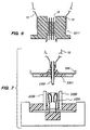
- Figure 7 illustrates the method of sealing a card edge type connector 2300.
- a sealing gasket 2301 is attached to the adapter 500 so that when the connector is plugged into the female half 2320 the gasket 2301 will be pressed tightly against the lip of the female half 2320 and the sealing ring 2330. To further block the leak paths in the female connector 2320 gel can be deposited into it.
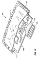
- Figure 8 illustrates a guide and latch mechanism that permits the active electronics 1000 to be plugged into the connector pins 16 protruding on the inside of the adapter 18.
- Guiding ribs 2210 are used to safely guide the active electronics 1000 into engagement with the connector pins 16 protruding on the inside of the adapter 18.
- a latching hook mechanism 2211 will then fall into a hole 2212 in the active electronics board holding it securely to the adapter 18.
- the latching hook 2211 includes a tactile and positive lock to prevent unwarranted unlocking of the board under vibrating conditions as well as providing a positive sense of when the board is locked in place to the connector.
- a compliant latch structure, e.g. spring loaded, and a compliant cushion, e.g. foam rubber, installed at the bottom, i.e. base, of the guiding ribs 2210 along and adjacent the rectangular face of the adapter 18 can be used to reduce forces on the active electronics 1000 when they are accidently dropped during handling.
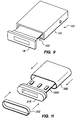
- Figure 9 illustrates a method of preventing this problem in situations where the module may receive rough handling.
- the adapter 18 could be designed to fit closely to the open end of the protective box 101 with provisions for screws or other fasteners to hold the parts together forming a finished electronic module 102. If screws are used, then the module 102 can easily be opened later to make repairs on the active electronics 1000.
- spacer blocks 25 (Fig. 1) are attached to the active electronics 1000 before sealing the sheet 10.
- the protective box 101 is blow molded and holes are provided to drain water and to permit the viewing of the lights on the active electronics 1000.
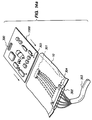
- FIG 10 illustrates the assembly of several modules 102 to a sealed back plane 203.
- Each back plane has several female connectors 204 electrically connected to a back plane circuit board and men potted to exclude moisture from the back side. Wires also connected to the backplane circuit board carry the signals to sealed terminal blocks 205.
- the protective box 101 has the disadvantage of reducing the heat transfer of the system and adding extra cost and bulk. In some cases, where only a moderate amount of mechanical protection is required, a more rigid sheet material 10 can be used, where the metal foil thickness is increased for greater bend resistance.
- Figure 11 illustrates a closure of this type were the heavy sheet material 200 is heat sealed into a tubular shape that will just fit over the adapter 218.
- a hot melt bond between the adapter 218 and the sheet material 200 can be made or preferably a heat shrinkable band 202 with a hot melt adhesive on the inside is shrunk over the joint between the adapter 218 and the sheet 200.
- the back end can be closed by heat sealing and folding in the manner of a milk carton or by inserting a plug with a shape similar to the adapter 218 and sealing in a like manner.
- Figure 12 illustrates a means of thermally coupling a hot component on the active electronics 1000 board through the sheet 10 and into a heat spreader 250 in the free stream air.
- Figure 13 illustrates the assembly of the parts in Figure 12. After sealing the sheet 10 the heat spreader 250 is clamped on to the active electronics 1000 at the point where the stabilizer blocks 25 are attached.
- thermally conductive gel pad 251 that has be preinstalled on the hot component 252 or inside the sheet material 10.
- a suitable thermally conductive gel 251 formulation for this purpose is described more thoroughly in US Patent 4,852,646, incorporated herein by reference.
- An additional pad of thermally conductive gel could also be applied between the outer surface of the sheet 10 and the heat spreader 250 to further improve the transfer of heat through the sheet 10 to the heat spreader.
- Figure 13c shows an alternative approach to remove heat from hot component 252.
- a bolt, 253, penetrates the flexible laminate and connects directly to 252.
- a sealing material seals between the flexible laminate and the hot component.
- Figure 14 illustrates a low cost method of providing packaging for this type of system.
- a connector 301 is attached to a wire harness 303 which is then insert molded into and adapter 302.
- To achieve a reliable seal it may be necessary to remove the insulation from the wire in the harness 303 in the area where it passes through the adapter 302 to block the flow of moisture under the insulation of the wires in harness 303.
- a curing blocking material could be used or a blocked wire that is fabricated with a blocking agent between the wire and the insulation.
- the active electronics 1000 is inserted into the open end of the packaging 100 until the latch features 304 molded onto the adapter 302 engage the holes 305 in the active electronics 1000. Once firmly attached in this manner, the connector 301 can be connected to the mating connector 300 on the active electronics 1000. After the desiccant/scavenger packet has been activated the open end of the sealed electronics packaging can be sealed as usual with a heat sealer.
- Figure 14b illustrates another embodiment and potentially a lower cost method of sealing the electronics.
- a flat cable 306 is connected to connector 307.
- the flexible laminate barrier is installed over the circuit board 1000 and heatsealed with hot melt adhesive to the flat cable 306 and fused to itself on both sides of 306 to form a complete moisture vapor barrier around 1000.
- FIG. 15 illustrates a simple method of accommodating this type of connector.
- a band of hot melt adhesive 420 is install around the card edge connector which as been fabricated to provide space for this application. Care must be take to assure that the contact fingers of the card edge connector 428 are not contaminated with this adhesive.
- the adhesive could be insert molded on the card edge extension.
- the sheet material 10 is welded into a closure 410 with one open side 414.
- the active electronics 1000 are inserted into the closure 410 and the open edge 414 is heat sealed closed over the hot melt adhesive 420.
- a modified bag sealer with appropriate relief for the area near the card edge connector is required for this operation.
- a card edge adapter could be fabricated using a small paddle card and a female card edge connector.
- the adapter would be preassembled into the closure 410 with the side of the closure opposite the adapter left open.
- the active electronics 1000 would be inserted into this open side and plugged into the female connector inside the closure. Then the open side could be heat sealed using conventional heat sealer.
- This alternative approach has the advantage of simplifying the heat sealing operation performed by final assembler.
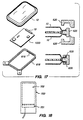
- Figures 16, 16a, and 16b illustrates another configuration of sealed electronics packaging for use with card edge connectors.
- An adapter 500 is sealed to the active electronics using and appropriate potting material 505.
- the closure 510 will seal to the adapter 500 which includes the active electronics board, at a U shaped member illustrated in figure 16a and 16b with a pressure ring 520 which will be ultimately encased between the hard outer box 530 and base member 500 more specifically, 16b illustrates in partial cross section the process of inserting the active electronics board 1000 and sealing to the base member 500.
- FIG. 17 A further alternative is illustrated in Figure 17.
- the adapter 618 is extended to from a complete ring around the active electronics 1000.
- the active electronics are plugged into the interior pins of the adapter connector 616 and then two sheets 10 are heat sealed or welded to the adapter ring 625.
- a forming tool 620 can be used to form a secure lip 630 to hold the sheets 10 in place.
- Figure 18 shows an improved packaging system for use in underground applications when the electronics will be possibly submerged under water for long periods of time.
- a bell jar 700 is placed over the sealed electronic modules 702 and the backplane 701. The belljar keeps liquid water from 701 and 702.
- the invention resides at least in part in the unexpected realization by the inventors that in spite of past thinking, the active electronics could be sealed in an appropriate laminate, protected from the environment, and still operate in harsh environments while permitting re-entry to the package by splitting of the package 100 upon return to the factory.
- the aluminum metallic sheet might be copper silver gold or other suitable material.
- the plastic laminate could be a one sheet fused to the metallic layer and folded over and fused to itself.
- the bag itself might have a sealed entry port in the event that the bag was not to be discarded upon requiring access to the active electronics to make repairs, and the like.
Landscapes
- Engineering & Computer Science (AREA)
- Microelectronics & Electronic Packaging (AREA)
- Casings For Electric Apparatus (AREA)
- Structures Or Materials For Encapsulating Or Coating Semiconductor Devices Or Solid State Devices (AREA)
- Connector Housings Or Holding Contact Members (AREA)
- Packages (AREA)
- Emergency Protection Circuit Devices (AREA)
- Packaging Frangible Articles (AREA)
- Heterocyclic Carbon Compounds Containing A Hetero Ring Having Oxygen Or Sulfur (AREA)
- Coloring Foods And Improving Nutritive Qualities (AREA)
- Sealing Material Composition (AREA)
- Pens And Brushes (AREA)
Applications Claiming Priority (5)
| Application Number | Priority Date | Filing Date | Title |
|---|---|---|---|
| US22614994A | 1994-04-11 | 1994-04-11 | |
| US226149 | 1994-04-11 | ||
| US397600 | 1995-03-02 | ||
| US08/397,600 US5739463A (en) | 1994-04-11 | 1995-03-02 | Sealed electronic packaging for environmental protection of active electronics |
| PCT/US1995/004291 WO1995028072A1 (en) | 1994-04-11 | 1995-04-06 | Sealed electronic packaging for environmental protection of active electronics |
Publications (2)
| Publication Number | Publication Date |
|---|---|
| EP0755618A1 EP0755618A1 (en) | 1997-01-29 |
| EP0755618B1 true EP0755618B1 (en) | 2000-06-21 |
Family
ID=26920250
Family Applications (1)
| Application Number | Title | Priority Date | Filing Date |
|---|---|---|---|
| EP95916228A Expired - Lifetime EP0755618B1 (en) | 1994-04-11 | 1995-04-06 | Sealed electronic packaging for environmental protection of active electronics |
Country Status (16)
| Country | Link |
|---|---|
| EP (1) | EP0755618B1 (pl) |
| JP (1) | JP3626499B2 (pl) |
| CN (1) | CN1149378A (pl) |
| AT (1) | ATE194052T1 (pl) |
| AU (1) | AU690262B2 (pl) |
| BR (1) | BR9507352A (pl) |
| CA (1) | CA2187653C (pl) |
| CZ (1) | CZ296496A3 (pl) |
| DE (1) | DE69517586T2 (pl) |
| ES (1) | ES2147286T3 (pl) |
| FI (1) | FI964054L (pl) |
| HU (1) | HUT76009A (pl) |
| IL (1) | IL113065A (pl) |
| PL (1) | PL175966B1 (pl) |
| SK (1) | SK130296A3 (pl) |
| WO (1) | WO1995028072A1 (pl) |
Cited By (3)
| Publication number | Priority date | Publication date | Assignee | Title |
|---|---|---|---|---|
| AU2012101888B4 (en) * | 2012-09-07 | 2013-07-11 | Apple Inc. | Compliant mount for connector |
| US8721356B2 (en) | 2012-09-11 | 2014-05-13 | Apple Inc. | Dock with compliant connector mount |
| US8986029B2 (en) | 2012-09-11 | 2015-03-24 | Apple Inc. | Dock connector with compliance mechanism |
Families Citing this family (18)
| Publication number | Priority date | Publication date | Assignee | Title |
|---|---|---|---|---|
| JP3538674B2 (ja) * | 1995-03-02 | 2004-06-14 | タイコ・エレクトロニクス・レイケム・ナムローゼ・フェンノートシャップ | 素子を環境から保護するための密封パッケージング |
| DE19634523B4 (de) * | 1996-08-27 | 2005-02-24 | Robert Bosch Gmbh | Verfahren zur Herstellung einer Anordnung von elektrischen und/oder optoelektronischen Bauteilen in einer gasdichten Verpackung und eine entsprechende Anordnung |
| US5968386A (en) * | 1997-12-18 | 1999-10-19 | Ford Motor Company | Method for protecting electronic components |
| JP4096605B2 (ja) * | 2002-04-23 | 2008-06-04 | 日本電気株式会社 | 半導体装置および半導体装置のシールド形成方法 |
| DE10247676A1 (de) * | 2002-10-12 | 2004-07-15 | Hella Kg Hueck & Co. | Elektrisches oder elektronisches Gerät mit einer Leiterplatte |
| US7576991B2 (en) | 2004-01-13 | 2009-08-18 | Taisei Plas Co., Ltd. | Electrical equipment for junction and method of manufacturing the same |
| RU2295207C1 (ru) * | 2005-07-25 | 2007-03-10 | Открытое акционерное общество "Научно-производственный комплекс "ЭЛАРА" | Корпус для электронных приборов |
| TWI340625B (en) | 2007-11-07 | 2011-04-11 | Wistron Corp | Shielding device and method of making the same |
| CN102202452B (zh) * | 2007-11-15 | 2014-07-09 | 纬创资通股份有限公司 | 一种防护装置 |
| JP2010232330A (ja) * | 2009-03-26 | 2010-10-14 | Autech Japan Inc | 強電体のケース構造 |
| DE102011004694A1 (de) | 2011-02-24 | 2012-08-30 | Robert Bosch Gmbh | Schaltungsanordnung, insbesondere ein Getriebesteuergerät, mit mindestens einem Deckel zur Kapselung eines Schaltungsträgers |
| JP5647648B2 (ja) | 2012-06-20 | 2015-01-07 | 富士フイルム株式会社 | 回路装置及びインクジェットヘッドアッセンブリ |
| ES1089931Y (es) * | 2013-08-21 | 2013-12-13 | Mendez Jordi Llanes | Sistema automático de regulación de volumen para fundas y/o contenedores herméticos destinados a la protección de aparatos electrónicos y/o eléctricos |
| WO2015199128A1 (ja) * | 2014-06-27 | 2015-12-30 | 日本電気株式会社 | 電子機器およびその製造方法 |
| DE202015101901U1 (de) * | 2015-04-17 | 2016-07-20 | Tridonic Gmbh & Co Kg | Gehäuse zur Aufnahme einer Elektronik-Baugruppe mit einer elektrischen Anschlussleitung |
| CN107924880B (zh) * | 2015-11-27 | 2020-11-24 | 京瓷株式会社 | 电子部件搭载用封装体以及电子装置 |
| JP7287796B2 (ja) * | 2019-03-08 | 2023-06-06 | 株式会社ミクニ | 電子部品モジュール及びそのコネクタケース |
| CN113727565B (zh) * | 2021-08-31 | 2022-12-09 | 青岛海信移动通信技术股份有限公司 | 密封连接结构以及智能终端设备 |
Family Cites Families (5)
| Publication number | Priority date | Publication date | Assignee | Title |
|---|---|---|---|---|
| US3909504A (en) * | 1973-11-05 | 1975-09-30 | Carrier Tel Corp America Inc | Ruggedized package for electronic components and the like |
| JPH0278372U (pl) * | 1988-12-06 | 1990-06-15 | ||
| JPH0634152Y2 (ja) * | 1988-12-08 | 1994-09-07 | 多機能カード | |
| DE4229727A1 (de) * | 1992-09-05 | 1994-03-10 | Bosch Gmbh Robert | Elektrisches Gerät, insbesondere Schalt- oder Steuergerät für Kraftfahrzeuge |
| US5285619A (en) * | 1992-10-06 | 1994-02-15 | Williams International Corporation | Self tooling, molded electronics packaging |
-
1995
- 1995-03-21 IL IL11306595A patent/IL113065A/xx not_active IP Right Cessation
- 1995-04-06 HU HU9602783A patent/HUT76009A/hu unknown
- 1995-04-06 CZ CZ962964A patent/CZ296496A3/cs unknown
- 1995-04-06 WO PCT/US1995/004291 patent/WO1995028072A1/en not_active Ceased
- 1995-04-06 AU AU22804/95A patent/AU690262B2/en not_active Ceased
- 1995-04-06 AT AT95916228T patent/ATE194052T1/de not_active IP Right Cessation
- 1995-04-06 BR BR9507352A patent/BR9507352A/pt not_active IP Right Cessation
- 1995-04-06 SK SK1302-96A patent/SK130296A3/sk unknown
- 1995-04-06 JP JP52645895A patent/JP3626499B2/ja not_active Expired - Fee Related
- 1995-04-06 PL PL95317048A patent/PL175966B1/pl unknown
- 1995-04-06 CA CA002187653A patent/CA2187653C/en not_active Expired - Fee Related
- 1995-04-06 CN CN95193246.2A patent/CN1149378A/zh active Pending
- 1995-04-06 ES ES95916228T patent/ES2147286T3/es not_active Expired - Lifetime
- 1995-04-06 FI FI964054A patent/FI964054L/fi unknown
- 1995-04-06 DE DE69517586T patent/DE69517586T2/de not_active Expired - Lifetime
- 1995-04-06 EP EP95916228A patent/EP0755618B1/en not_active Expired - Lifetime
Cited By (6)
| Publication number | Priority date | Publication date | Assignee | Title |
|---|---|---|---|---|
| AU2012101888B4 (en) * | 2012-09-07 | 2013-07-11 | Apple Inc. | Compliant mount for connector |
| US8535102B1 (en) | 2012-09-07 | 2013-09-17 | Apple Inc. | Compliant mount for connector |
| US9160124B2 (en) | 2012-09-07 | 2015-10-13 | Apple Inc. | Compliant mount for connector |
| US8721356B2 (en) | 2012-09-11 | 2014-05-13 | Apple Inc. | Dock with compliant connector mount |
| US8986029B2 (en) | 2012-09-11 | 2015-03-24 | Apple Inc. | Dock connector with compliance mechanism |
| US9261919B2 (en) | 2012-09-11 | 2016-02-16 | Apple Inc. | Dock with compliant connector mount |
Also Published As
| Publication number | Publication date |
|---|---|
| CN1149378A (zh) | 1997-05-07 |
| FI964054A7 (fi) | 1996-12-10 |
| FI964054L (fi) | 1996-12-10 |
| PL175966B1 (pl) | 1999-03-31 |
| IL113065A0 (en) | 1995-06-29 |
| BR9507352A (pt) | 1997-09-23 |
| PL317048A1 (en) | 1997-03-03 |
| JP3626499B2 (ja) | 2005-03-09 |
| ATE194052T1 (de) | 2000-07-15 |
| WO1995028072A1 (en) | 1995-10-19 |
| MX9604718A (es) | 1998-05-31 |
| IL113065A (en) | 2000-06-01 |
| CA2187653A1 (en) | 1995-10-19 |
| JPH09512134A (ja) | 1997-12-02 |
| ES2147286T3 (es) | 2000-09-01 |
| CZ296496A3 (en) | 1997-10-15 |
| DE69517586T2 (de) | 2001-03-08 |
| AU690262B2 (en) | 1998-04-23 |
| AU2280495A (en) | 1995-10-30 |
| FI964054A0 (fi) | 1996-10-10 |
| HU9602783D0 (en) | 1996-11-28 |
| HUT76009A (en) | 1997-06-30 |
| SK130296A3 (en) | 1997-10-08 |
| CA2187653C (en) | 2005-01-11 |
| EP0755618A1 (en) | 1997-01-29 |
| DE69517586D1 (de) | 2000-07-27 |
Similar Documents
| Publication | Publication Date | Title |
|---|---|---|
| US5739463A (en) | Sealed electronic packaging for environmental protection of active electronics | |
| EP0755618B1 (en) | Sealed electronic packaging for environmental protection of active electronics | |
| EP0635193B1 (en) | A flexible device for encapsulating electronic components | |
| US5689878A (en) | Method for protecting electronic circuit components | |
| EP0335430B1 (en) | Method for protecting elements enclosed by a housing against the influence of moisture | |
| JP3604383B2 (ja) | ゲル充填電気コネクタ | |
| CN112117583B (zh) | 具有防水结构的连接器与制造方法 | |
| WO2009026431A1 (en) | Fire resistant enclosure for a data storage device having heat sink capabilities and method for making the same | |
| US8861210B2 (en) | Bucket-style fire resistant enclosure and a method for making the same | |
| CN111509441B (zh) | 加固型电插座 | |
| CN1412866A (zh) | 电池组 | |
| US6590158B1 (en) | Pressure container with layered seal assembly | |
| CN1198262A (zh) | 密封互联装置 | |
| EP0812527B2 (en) | Sealed packaging for environmental protection of electronics | |
| MXPA96004718A (en) | Sealed electronics packing for electronic-environmental protection act | |
| EP0286440A2 (en) | Connector assembly | |
| JP2003086925A (ja) | 防湿構造付プリント基板、及びその製造方法 | |
| CA2155706C (en) | Environmental protector | |
| JPS63148807A (ja) | ガス絶縁電器の事故検出装置 |
Legal Events
| Date | Code | Title | Description |
|---|---|---|---|
| PUAI | Public reference made under article 153(3) epc to a published international application that has entered the european phase |
Free format text: ORIGINAL CODE: 0009012 |
|
| 17P | Request for examination filed |
Effective date: 19961015 |
|
| AK | Designated contracting states |
Kind code of ref document: A1 Designated state(s): AT BE CH DE DK ES FR GB GR IE IT LI NL PT SE |
|
| 17Q | First examination report despatched |
Effective date: 19980217 |
|
| GRAG | Despatch of communication of intention to grant |
Free format text: ORIGINAL CODE: EPIDOS AGRA |
|
| GRAG | Despatch of communication of intention to grant |
Free format text: ORIGINAL CODE: EPIDOS AGRA |
|
| GRAH | Despatch of communication of intention to grant a patent |
Free format text: ORIGINAL CODE: EPIDOS IGRA |
|
| GRAH | Despatch of communication of intention to grant a patent |
Free format text: ORIGINAL CODE: EPIDOS IGRA |
|
| GRAA | (expected) grant |
Free format text: ORIGINAL CODE: 0009210 |
|
| AK | Designated contracting states |
Kind code of ref document: B1 Designated state(s): AT BE CH DE DK ES FR GB GR IE IT LI NL PT SE |
|
| PG25 | Lapsed in a contracting state [announced via postgrant information from national office to epo] |
Ref country code: LI Free format text: LAPSE BECAUSE OF FAILURE TO SUBMIT A TRANSLATION OF THE DESCRIPTION OR TO PAY THE FEE WITHIN THE PRESCRIBED TIME-LIMIT Effective date: 20000621 Ref country code: CH Free format text: LAPSE BECAUSE OF FAILURE TO SUBMIT A TRANSLATION OF THE DESCRIPTION OR TO PAY THE FEE WITHIN THE PRESCRIBED TIME-LIMIT Effective date: 20000621 Ref country code: AT Free format text: LAPSE BECAUSE OF FAILURE TO SUBMIT A TRANSLATION OF THE DESCRIPTION OR TO PAY THE FEE WITHIN THE PRESCRIBED TIME-LIMIT Effective date: 20000621 |
|
| REF | Corresponds to: |
Ref document number: 194052 Country of ref document: AT Date of ref document: 20000715 Kind code of ref document: T |
|
| REG | Reference to a national code |
Ref country code: CH Ref legal event code: EP |
|
| REG | Reference to a national code |
Ref country code: IE Ref legal event code: FG4D |
|
| REF | Corresponds to: |
Ref document number: 69517586 Country of ref document: DE Date of ref document: 20000727 |
|
| ET | Fr: translation filed | ||
| REG | Reference to a national code |
Ref country code: ES Ref legal event code: FG2A Ref document number: 2147286 Country of ref document: ES Kind code of ref document: T3 |
|
| ITF | It: translation for a ep patent filed | ||
| PG25 | Lapsed in a contracting state [announced via postgrant information from national office to epo] |
Ref country code: PT Free format text: LAPSE BECAUSE OF FAILURE TO SUBMIT A TRANSLATION OF THE DESCRIPTION OR TO PAY THE FEE WITHIN THE PRESCRIBED TIME-LIMIT Effective date: 20000921 Ref country code: DK Free format text: LAPSE BECAUSE OF FAILURE TO SUBMIT A TRANSLATION OF THE DESCRIPTION OR TO PAY THE FEE WITHIN THE PRESCRIBED TIME-LIMIT Effective date: 20000921 |
|
| PG25 | Lapsed in a contracting state [announced via postgrant information from national office to epo] |
Ref country code: GR Free format text: LAPSE BECAUSE OF FAILURE TO SUBMIT A TRANSLATION OF THE DESCRIPTION OR TO PAY THE FEE WITHIN THE PRESCRIBED TIME-LIMIT Effective date: 20000922 |
|
| REG | Reference to a national code |
Ref country code: CH Ref legal event code: PL |
|
| PG25 | Lapsed in a contracting state [announced via postgrant information from national office to epo] |
Ref country code: IE Free format text: LAPSE BECAUSE OF NON-PAYMENT OF DUE FEES Effective date: 20010406 |
|
| PLBE | No opposition filed within time limit |
Free format text: ORIGINAL CODE: 0009261 |
|
| STAA | Information on the status of an ep patent application or granted ep patent |
Free format text: STATUS: NO OPPOSITION FILED WITHIN TIME LIMIT |
|
| 26N | No opposition filed | ||
| REG | Reference to a national code |
Ref country code: GB Ref legal event code: IF02 |
|
| REG | Reference to a national code |
Ref country code: IE Ref legal event code: MM4A |
|
| PGFP | Annual fee paid to national office [announced via postgrant information from national office to epo] |
Ref country code: ES Payment date: 20110426 Year of fee payment: 17 Ref country code: FR Payment date: 20110504 Year of fee payment: 17 Ref country code: SE Payment date: 20110425 Year of fee payment: 17 Ref country code: DE Payment date: 20110427 Year of fee payment: 17 |
|
| PGFP | Annual fee paid to national office [announced via postgrant information from national office to epo] |
Ref country code: NL Payment date: 20110429 Year of fee payment: 17 Ref country code: BE Payment date: 20110426 Year of fee payment: 17 Ref country code: GB Payment date: 20110426 Year of fee payment: 17 |
|
| PGFP | Annual fee paid to national office [announced via postgrant information from national office to epo] |
Ref country code: IT Payment date: 20110423 Year of fee payment: 17 |
|
| BERE | Be: lapsed |
Owner name: *RAYCHEM CORP. Effective date: 20120430 |
|
| REG | Reference to a national code |
Ref country code: NL Ref legal event code: V1 Effective date: 20121101 |
|
| REG | Reference to a national code |
Ref country code: SE Ref legal event code: EUG |
|
| GBPC | Gb: european patent ceased through non-payment of renewal fee |
Effective date: 20120406 |
|
| REG | Reference to a national code |
Ref country code: FR Ref legal event code: ST Effective date: 20121228 |
|
| PG25 | Lapsed in a contracting state [announced via postgrant information from national office to epo] |
Ref country code: BE Free format text: LAPSE BECAUSE OF NON-PAYMENT OF DUE FEES Effective date: 20120430 Ref country code: GB Free format text: LAPSE BECAUSE OF NON-PAYMENT OF DUE FEES Effective date: 20120406 |
|
| REG | Reference to a national code |
Ref country code: DE Ref legal event code: R119 Ref document number: 69517586 Country of ref document: DE Effective date: 20121101 |
|
| PG25 | Lapsed in a contracting state [announced via postgrant information from national office to epo] |
Ref country code: SE Free format text: LAPSE BECAUSE OF NON-PAYMENT OF DUE FEES Effective date: 20120407 Ref country code: FR Free format text: LAPSE BECAUSE OF NON-PAYMENT OF DUE FEES Effective date: 20120430 Ref country code: IT Free format text: LAPSE BECAUSE OF NON-PAYMENT OF DUE FEES Effective date: 20120406 |
|
| PG25 | Lapsed in a contracting state [announced via postgrant information from national office to epo] |
Ref country code: NL Free format text: LAPSE BECAUSE OF NON-PAYMENT OF DUE FEES Effective date: 20121101 |
|
| REG | Reference to a national code |
Ref country code: ES Ref legal event code: FD2A Effective date: 20130715 |
|
| PG25 | Lapsed in a contracting state [announced via postgrant information from national office to epo] |
Ref country code: ES Free format text: LAPSE BECAUSE OF NON-PAYMENT OF DUE FEES Effective date: 20120407 |
|
| PG25 | Lapsed in a contracting state [announced via postgrant information from national office to epo] |
Ref country code: DE Free format text: LAPSE BECAUSE OF NON-PAYMENT OF DUE FEES Effective date: 20121101 |