EP0755062B1 - Gekapselte Spannungswandleranordnung für Schaltanlagen mit mehreren Anlagenfeldern - Google Patents
Gekapselte Spannungswandleranordnung für Schaltanlagen mit mehreren Anlagenfeldern Download PDFInfo
- Publication number
- EP0755062B1 EP0755062B1 EP95110858A EP95110858A EP0755062B1 EP 0755062 B1 EP0755062 B1 EP 0755062B1 EP 95110858 A EP95110858 A EP 95110858A EP 95110858 A EP95110858 A EP 95110858A EP 0755062 B1 EP0755062 B1 EP 0755062B1
- Authority
- EP
- European Patent Office
- Prior art keywords
- housing
- core
- axes
- transformer
- disposed
- Prior art date
- Legal status (The legal status is an assumption and is not a legal conclusion. Google has not performed a legal analysis and makes no representation as to the accuracy of the status listed.)
- Expired - Lifetime
Links
- 238000009434 installation Methods 0.000 title description 2
- 230000015572 biosynthetic process Effects 0.000 claims description 5
- 229910018503 SF6 Inorganic materials 0.000 description 1
- 230000015556 catabolic process Effects 0.000 description 1
- 239000004020 conductor Substances 0.000 description 1
- 238000010292 electrical insulation Methods 0.000 description 1
- 230000001771 impaired effect Effects 0.000 description 1
- SFZCNBIFKDRMGX-UHFFFAOYSA-N sulfur hexafluoride Chemical compound FS(F)(F)(F)(F)F SFZCNBIFKDRMGX-UHFFFAOYSA-N 0.000 description 1
- 229960000909 sulfur hexafluoride Drugs 0.000 description 1
Images


Classifications
-
- H—ELECTRICITY
- H01—ELECTRIC ELEMENTS
- H01F—MAGNETS; INDUCTANCES; TRANSFORMERS; SELECTION OF MATERIALS FOR THEIR MAGNETIC PROPERTIES
- H01F27/00—Details of transformers or inductances, in general
- H01F27/02—Casings
-
- H—ELECTRICITY
- H01—ELECTRIC ELEMENTS
- H01F—MAGNETS; INDUCTANCES; TRANSFORMERS; SELECTION OF MATERIALS FOR THEIR MAGNETIC PROPERTIES
- H01F38/00—Adaptations of transformers or inductances for specific applications or functions
- H01F38/20—Instruments transformers
- H01F38/22—Instruments transformers for single phase AC
- H01F38/24—Voltage transformers
- H01F38/26—Constructions
-
- H—ELECTRICITY
- H01—ELECTRIC ELEMENTS
- H01F—MAGNETS; INDUCTANCES; TRANSFORMERS; SELECTION OF MATERIALS FOR THEIR MAGNETIC PROPERTIES
- H01F38/00—Adaptations of transformers or inductances for specific applications or functions
- H01F38/20—Instruments transformers
- H01F38/38—Instruments transformers for polyphase AC
Definitions
- the invention relates to an encapsulated Voltage converter arrangement for switchgear with several plant fields that run alongside each other extending system axes are arranged, according to Preamble of claim 1.
- DE-U-9 209 167 is an encapsulated one Voltage converter arrangement known in the three in section round or elongated housing for one Voltage transformers are arranged side by side. If each voltage converter has its own housing while there are no particular problems with each other electrical insulation, but that's the arrangement also not designed multi-phase. On the other hand, that would be Building a multi-phase arrangement is no longer compact, if along the lines of this release a separate housing for each Voltage converter would be designed.
- JP-A-56 114308 is known to have three in a single housing To accommodate voltage transformers.
- the Core axes of the magnetic cores transverse to the longitudinal axis of an im Section rectangular case aligned and in Are arranged one behind the other in the longitudinal direction.
- the coils come very close so that the Dielectric strength can be impaired.
- the core axes again aligned parallel to each other, but the Voltage transformers are in a triangular formation housed in an average circular housing.
- DE-C-0 576 081 is a Voltage transformer arrangement with three in a row arranged voltage transformers known in the also the core axes of the magnetic cores transverse to Longitudinal axis of an elongated housing aligned and are arranged one behind the other in the longitudinal direction.
- the cores are by side, in Core legs extending in the longitudinal direction with one another connected. But here too is the distance between the Coils very low, so that the dielectric strength may be affected.
- the invention has for its object a encapsulated voltage transformer arrangement for switchgear to indicate with several plant fields, which a small Has housing width and still a sufficient Distance between the live components guaranteed, and to specify a switchgear these encapsulated voltage converter arrangements.
- the solution according to the invention is that the Voltage converters are also parallel to each other aligned but offset from each other.
- This arrangement uses both the case length and the case width are optimal without the coils arranged on the cores would be close to the housing walls.
- the The distances between the coils are large enough to To prevent voltage flashovers. This results in the advantage that switchgear with several Plant fields also several converter housings in one shorter distance can be arranged. This makes the switchgear more compact without Cut back on dielectric strength should be.
- this is Transducer housing elliptical in section, four Rectangularly arranged and rounded corners indicated are.
- This form of housing is particularly recommended if the interior of the converter housing with a Insulating gas, for example sulfur hexafluoride, under high pressure to be filled.
- the curved Housing walls only require a small wall thickness.
- the long sides are also flattened. This Housing shape is particularly advantageous if the Case length is not very much larger than that Case width.
- the task is the longitudinal axis of the housing Transducer housing substantially perpendicular to one level determined by the system axes and the voltage transformers are transverse with their core axes aligned to the longitudinal axis of the housing and in the longitudinal direction arranged one above the other, the cores being separated by two lateral, longitudinal core legs are integrally connected.
- the converter housing with its In this embodiment, the longitudinal axis of the housing is vertical, so that it can be recommended for switchgear, their installation space in width, i.e. across to the Plant axes is restricted, however, where vertical enough space is available upwards.
- the invention also relates to a Switchgear designed according to the invention Voltage converter arrangements.
- a Switchgear designed according to the invention Voltage converter arrangements.
- Such an arrangement is already due the inventive design of the Voltage converter arrangements more compact than known ones Switchgear.
- the converter housing 1 is essentially elliptical and has four rectangularly arranged and rounded corners 7. Two side walls 8 are curved and extend essentially in the direction of a Longitudinal axis 9.
- the voltage converters 2, 3, 4 are elongated Formation in the direction of the housing longitudinal axis 9 arranged one behind the other, the core axes 10, 11, 12 of the cores 5 parallel to the longitudinal axis 9 of the housing lie.
- the core axes 10 and 12 of a first and one third core 5 are laterally opposite to the left Longitudinal axis 9 shifted.
- a second middle one Core 5 with core axis 11 is on the right side shifted relative to the longitudinal axis 9 of the housing.
- the free ends 13, 14, 15, 16 of the cores 5 side by side and overlap lengthways.
- the Core axes 10, 11, 12 transverse to the longitudinal axis 9 of the housing aligned and the voltage converters 2, 3, 4 in turn arranged one behind the other in the longitudinal direction.
- the three Cores 5 are through two lateral, parallel to Longitudinal axis 9 of the core legs 17, 18 connected in one piece.
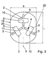
- Fig. 3 shows a converter housing 19, in which the Housing length l is not very much larger than that Housing width b is. Beyond that it is Transducer housing 19 flattened on its long sides, so that two straight, parallel side walls 20th arise.
- the three voltage converters 2, 3, 4 are star-shaped with radial core axes 10, 11, 12 arranged, the core axis 10 of a first Voltage converter 2 parallel to the longitudinal axis 9 of the housing is aligned and coincides with this.
- the two other core axes 11, 12 of the other two Voltage converters 3, 4 each point to the first Core axis 10 at an angle W of more than 120 °.
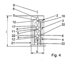
- the converter housing 21 shown in Fig. 4 is in essentially cylindrical, again the Housing length l larger than that of the cylinder diameter corresponding housing width b is. They are here too Voltage converters 2, 3, 4 with their core axes 10, 11, 12 arranged transversely to the longitudinal axis 9 of the housing, the Cores 5 through two lateral, parallel to Longitudinal axis 9 of the core legs 17, 18 are integrally connected.
- Embodiment of the invention are Longitudinal axis 9 of the transducer housing 21 perpendicular to a level determined by the system axes A, B, C aligned. In Fig. 7 this level corresponds to the Paper plane on which the housing longitudinal axes 9 are perpendicular stand.
- the cylindrical converter housing 21 then protrudes vertically upwards.
- the cylinder diameter of the Transducer housing 21 determines the housing width b, which in turn turns out to be advantageously small, since this one arrangement according to the invention within the circular Cross section accommodated only a voltage converter must be, since the three voltage converters 2, 3, 4 one above the other in the direction of the cylinder longitudinal axis are arranged.
- the three voltage transformers within the circular housing cross section side by side arranged in a star shape, resulting in a larger one Housing diameter and thus a larger one Housing width b results.
Landscapes
- Engineering & Computer Science (AREA)
- Power Engineering (AREA)
- Patch Boards (AREA)
- Dc-Dc Converters (AREA)
- Gas-Insulated Switchgears (AREA)
Description
- Fig. 1:
- eine schematische Darstellung einer erfindungsgemäßen Spannungswandleranordnung mit geschnittenem Wandlergehäuse in einer ersten Ausgestaltungsform und einer Draufsicht auf die Spannungswandler in einer bevorzugten Anordnung,
- Fig. 2:
- wie Fig. 1 mit einer zweiten Anordnung der Spannungswandler,
- Fig. 3:
- wie Fig. 1 mit einer zweiten Ausgestaltungsform der Wandlergehäuses und einer dritten Anordnung der Spannungswandler,
- Fig. 4:
- wie Fig. 1 mit einer weiteren Ausgestaltungsform des Wandlergehäuses und einer weiteren Anordnung der Spannungswandler,
- Fig. 5:
- eine schematische Darstellung einer Anordnung von Wandlergehäusen gemäß der Fig. 1 und 2,
- Fig. 6:
- dieselbe Anordnungsform von anderen Wandlergehäusen gem. Fig. 3,
- Fig. 7:
- eine entsprechende Anordnung von Wandlergehäusen gem. Fig. 4.
- 1
- Wandlergehäuse
- 2
- Spannungswandler
- 3
- Spannungswandler
- 4
- Spannungswandler
- 5
- Kern
- 6
- Spule
- 7
- Ecken
- 8
- Seitenwände
- 9
- Gehäuselängsachse
- 10
- Kernachse
- 11
- Kernachse
- 12
- Kernachse
- 13
- freies Ende
- 14
- freies Ende
- 15
- freies Ende
- 16
- freies Ende
- 17
- Kernschenkel
- 18
- Kernschenkel
- 19
- Wandlergehäuse
- 20
- Seitenwände
- 21
- Wandlergehäuse
- 22
- Leiter
- A
- Anlagenachse
- B
- Anlagenachse
- C
- Anlagenachse
- l
- Gehäuselänge
- b
- Gehäusebreite
- t
- Abstand
- W
- Winkel
Claims (6)
- Gekapselte Spannungswandleranordnung für Schaltanlagen mit mehreren Anlagenfeldern, die entlang von nebeneinander verlaufenden Anlagenachsen (A, B, C) angeordnet sind; mit einem Wandlergehäuse (1. 19, 21) mit drei Spannungswandlern (2, 3, 4), die jeweils eine auf einem längs einer Kernachse (10, 11, 12) ausgerichteten Kern (5) angeordnete Spule (6) aufweisen, wobei das Wandlergehäuse (1, 19, 21) im Schnitt länglich mit einer größeren Gehäuselänge (l) und einer kleineren Gehäusebreite (b) ausgestaltet ist, wobei die Gehäusebreite (b) quer zu den Anlagenachsen (A, B, C) und eine Gehäuselängsachse (9) im wesentlichen parallel zu den Anlagenachsen (A, B, C) ausgerichtet ist und wobei die Spannungswandler (2, 3, 4) im Wandlergehäuse (1, 19, 21) in länglicher Formation in bezug auf die Gehäuselänge (l) angeordnet sind, wobei die Spannungswandler (2, 3, 4) mit ihren Kernachsen (10, 11, 12) parallel zur Gehäuselängsachse (9) ausgerichtet und in Längsrichtung hintereinander angeordnet sind, wobei ein erster und ein dritter Kern (5) mit den Kernachsen (10, 12) seitlich neben der Gehäuselängsachse (9) zur einen Seite hin und ein zweiter, mittlerer Kern (5) mit der Kernachse (11) zur anderen Seite hin versetzt ist, so daß sich die nebeneinanderliegenden freien Enden (13, 14, 15, 16) der Kerne (5) in Längsrichtung überlappen.
- Gekapselte Spannungswandleranordnung für Schaltanlagen mit mehreren Anlagenfeldern, die entlang von nebeneinander verlaufenden Anlagenachsen (A, B, C) angeordnet sind; mit einem Wandlergehäuse (1. 19, 21) mit drei Spannungswandlern (2, 3, 4), die jeweils eine auf einem längs einer Kernachse (10, 11, 12) ausgerichteten Kern (5) angeordnete Spule (6) aufweisen, wobei das Wandlergehäuse (1, 19, 21) im Schnitt länglich mit einer größeren Gehäuselänge (l) und einer kleineren Gehäusebreite (b) ausgestaltet ist, wobei die Gehäusebreite (b) quer zu den Anlagenachsen (A, B, C) und eine Gehäuselängsachse (9) im wesentlichen parallel zu den Anlagenachsen (A, B, C) ausgerichtet ist und wobei die Spannungswandler (2, 3, 4) im Wandlergehäuse (1, 19, 21) in länglicher Formation in bezug auf die Gehäuselänge (l) angeordnet sind, wobei die drei Spannungswandler (2, 3, 4) sternförmig mit radialen Kernachsen (10, 11, 12) angeordnet sind, wobei die Kernachse (10) eines ersten Spannungswandlers (2) im wesentlichen parallel zur Gehäuselängsachse (9) ausgerichtet ist und die beiden anderen Kernachsen (11, 12) jeweils einen Winkel (W) von mehr als 120° zur ersten Kernachse (10) aufweisen.
- Gekapselte Spannungswandleranordnung nach Anspruch 1 oder 2, dadurch gekennzeichnet, daß das Wandlergehäuse (1) im Horizontalschnitt im wesentlichen elliptisch ausgestaltet ist, wobei vier rechteckig angeordnete und abgerundete Ecken (7) angedeutet sind.
- Gekapselte Spannungswandleranordnung nach Anspruch 3, dadurch gekennzeichnet, daß das Wandlergehäuse (19) im Horizontalschnitt zusätzlich an den Längsseiten abgeflacht ist.
- Gekapselte Spannungswandleranordnung für Schaltanlagen mit mehreren Anlagenfeldern, die entlang von nebeneinander verlaufenden Anlagenachsen (A, B, C) angeordnet sind; mit einem Wandlergehäuse (1. 19, 21) mit drei Spannungswandlern (2, 3, 4), die jeweils eine auf einem längs einer Kernachse (10, 11, 12) ausgerichteten Kern (5) angeordnete Spule (6) aufweisen, wobei das Wandlergehäuse (1, 19, 21) im Schnitt länglich mit einer größeren Gehäuselänge (l) und einer kleineren, quer zu den Anlagenachsen (A, B, C) ausgerichteten Gehäusebreite (b) ausgestaltet ist, und wobei die Spannungswandler (2, 3, 4) im Wandlergehäuse (1, 19, 21) in länglicher Formation in bezug auf die Gehäuselänge (l) angeordnet sind, wobei die Gehäuselängsachse (9) des Wandlergehäuses (21) im wesentlichen senkrecht zu einer durch die Anlagenachsen (A, B, C) bestimmten Ebene ausgerichtet ist und wobei die Spannungswandler (2, 3, 4) mit ihren Kernachsen (10, 11, 12) quer zur Gehäuselängsachse (9) ausgerichtet und in Längsrichtung übereinander angeordnet sind, wobei die Kerne (5) durch zwei seitliche, in Längsrichtung verlaufende Kernschenkel (17, 18) einstückig miteinander verbunden sind.
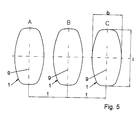
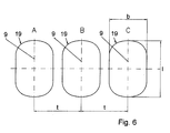
- Schaltanlage mit mehreren Anlagenfeldern, die entlang von nebeneinander verlaufenden Anlagenachsen (A, B, C) angeordnet sind, und mit gekapselten Spannungswandleranordnungen nach einem der vorhergehenden Ansprüche, dadurch gekennzeichnet, daß die Wandlergehäuse (1, 19, 21) in Querrichtung zu den Anlagenachsen (A, B, C) nebeneinander angeordnet sind.
Priority Applications (3)
| Application Number | Priority Date | Filing Date | Title |
|---|---|---|---|
| EP95110858A EP0755062B1 (de) | 1995-07-12 | 1995-07-12 | Gekapselte Spannungswandleranordnung für Schaltanlagen mit mehreren Anlagenfeldern |
| DE59505209T DE59505209D1 (de) | 1995-07-12 | 1995-07-12 | Gekapselte Spannungswandleranordnung für Schaltanlagen mit mehreren Anlagenfeldern |
| AT95110858T ATE177249T1 (de) | 1995-07-12 | 1995-07-12 | Gekapselte spannungswandleranordnung für schaltanlagen mit mehreren anlagenfeldern |
Applications Claiming Priority (1)
| Application Number | Priority Date | Filing Date | Title |
|---|---|---|---|
| EP95110858A EP0755062B1 (de) | 1995-07-12 | 1995-07-12 | Gekapselte Spannungswandleranordnung für Schaltanlagen mit mehreren Anlagenfeldern |
Publications (2)
| Publication Number | Publication Date |
|---|---|
| EP0755062A1 EP0755062A1 (de) | 1997-01-22 |
| EP0755062B1 true EP0755062B1 (de) | 1999-03-03 |
Family
ID=8219428
Family Applications (1)
| Application Number | Title | Priority Date | Filing Date |
|---|---|---|---|
| EP95110858A Expired - Lifetime EP0755062B1 (de) | 1995-07-12 | 1995-07-12 | Gekapselte Spannungswandleranordnung für Schaltanlagen mit mehreren Anlagenfeldern |
Country Status (3)
| Country | Link |
|---|---|
| EP (1) | EP0755062B1 (de) |
| AT (1) | ATE177249T1 (de) |
| DE (1) | DE59505209D1 (de) |
Families Citing this family (1)
| Publication number | Priority date | Publication date | Assignee | Title |
|---|---|---|---|---|
| EP2346128B1 (de) * | 2010-01-18 | 2012-11-21 | ABB Technology AG | Gasisolierter Sensormodul |
Family Cites Families (5)
| Publication number | Priority date | Publication date | Assignee | Title |
|---|---|---|---|---|
| DE576081C (de) * | 1929-05-01 | 1933-05-08 | Koch & Sterzel Akt Ges | Hochspannungstransformator, insbesondere Spannungswandler, dessen Oberspannungswicklung in einem einteiligen Spulenkasten aus Isolierwerkstoff untergebracht ist |
| DE701383C (de) * | 1938-11-23 | 1941-01-15 | Aeg | Durchfuehrungsstromwandler |
| DE904074C (de) * | 1944-06-18 | 1954-02-15 | Koch & Sterzel Ag | Trockenspannungswandler |
| JPS56114308A (en) * | 1980-02-14 | 1981-09-08 | Nissin Electric Co Ltd | Multiphase voltage transformer |
| DE9209167U1 (de) * | 1992-07-08 | 1992-11-26 | Kommanditgesellschaft Ritz Messwandler GmbH & Co, 20251 Hamburg | Spannungswandler für metallgekapselte Schaltanlagen |
-
1995
- 1995-07-12 EP EP95110858A patent/EP0755062B1/de not_active Expired - Lifetime
- 1995-07-12 DE DE59505209T patent/DE59505209D1/de not_active Expired - Lifetime
- 1995-07-12 AT AT95110858T patent/ATE177249T1/de not_active IP Right Cessation
Also Published As
| Publication number | Publication date |
|---|---|
| ATE177249T1 (de) | 1999-03-15 |
| DE59505209D1 (de) | 1999-04-08 |
| EP0755062A1 (de) | 1997-01-22 |
Similar Documents
| Publication | Publication Date | Title |
|---|---|---|
| DE2411246C3 (de) | Drehstromtransformator | |
| DE69402668T2 (de) | Hochspannungsfilter zur Filtrierung der Oberwellensignale in einem elektrischen Netzwerk | |
| EP0793243A1 (de) | Transformator | |
| DE3017561C2 (de) | Schaltgerät | |
| EP1249910A2 (de) | Hochspannungs-Leistungsschalter für eine druckgasisolierte Schaltanlage | |
| DE4210370A1 (de) | Hochspannungsschaltfeld | |
| EP0755062B1 (de) | Gekapselte Spannungswandleranordnung für Schaltanlagen mit mehreren Anlagenfeldern | |
| DE69709866T2 (de) | Filterausrüstung | |
| EP0986822B1 (de) | Elektromagnetisches schaltgerät mit mehrteiligem gehäuse | |
| EP4115435B1 (de) | Elektrisches gerät mit beulenkessel | |
| DE3318229A1 (de) | Gehaeuse fuer hochspannungsschalter | |
| CH688116A5 (de) | Stromkompensierte Mehrfachdrossel in Kompaktbauweise. | |
| DE2931000C2 (de) | Stufenschalter für Stufentransformatoren mit einem Träger für Polungswiderstände | |
| DE102004008961B4 (de) | Spulenkörper für geschlossenen magnetischen Kern und daraus hergestellte Entstördrossel | |
| DE2816356C2 (de) | Primärseitig umschaltbarer Stromwandler | |
| EP0813266A2 (de) | Mikrowellenfilter, bestehend aus mehreren Koaxial-Resonatoren | |
| EP0986123A2 (de) | Übergang zwischen zwei um 45 gegeneinander verdrehten Quadrathohlleitern | |
| DE1590276C3 (de) | Mittel- bzw. Hochspannungsverteilungsanordnung | |
| EP0102941B1 (de) | Drilleiterwicklung | |
| EP0276419B1 (de) | Ringkerntransformator mit mindestens zwei Wicklungen | |
| DE102010004971A1 (de) | Vorrichtung für eine Schaltanlage | |
| DE909224C (de) | Stabwicklung, deren Spulenseiten aus flachen Staeben bestehen und deren Stirnverbindungen durch Aufbiegen der geschlitzten Stabenden entstehen | |
| EP2273525A1 (de) | Elektrischer Leistungsschalter | |
| DE2108152C3 (de) | Hochspannungstransformatoranordnung in Isoliermantelbauweise | |
| EP0710964A2 (de) | Transformator zum Erzeugen zweier Hochspannungen von untereinander hoher Potentialdifferenz |
Legal Events
| Date | Code | Title | Description |
|---|---|---|---|
| PUAI | Public reference made under article 153(3) epc to a published international application that has entered the european phase |
Free format text: ORIGINAL CODE: 0009012 |
|
| AK | Designated contracting states |
Kind code of ref document: A1 Designated state(s): AT BE CH DE FR GB IT LI SE |
|
| 17P | Request for examination filed |
Effective date: 19970628 |
|
| 17Q | First examination report despatched |
Effective date: 19970801 |
|
| GRAG | Despatch of communication of intention to grant |
Free format text: ORIGINAL CODE: EPIDOS AGRA |
|
| GRAG | Despatch of communication of intention to grant |
Free format text: ORIGINAL CODE: EPIDOS AGRA |
|
| GRAH | Despatch of communication of intention to grant a patent |
Free format text: ORIGINAL CODE: EPIDOS IGRA |
|
| GRAH | Despatch of communication of intention to grant a patent |
Free format text: ORIGINAL CODE: EPIDOS IGRA |
|
| GRAA | (expected) grant |
Free format text: ORIGINAL CODE: 0009210 |
|
| AK | Designated contracting states |
Kind code of ref document: B1 Designated state(s): AT BE CH DE FR GB IT LI SE |
|
| REF | Corresponds to: |
Ref document number: 177249 Country of ref document: AT Date of ref document: 19990315 Kind code of ref document: T |
|
| REG | Reference to a national code |
Ref country code: CH Ref legal event code: EP |
|
| REF | Corresponds to: |
Ref document number: 59505209 Country of ref document: DE Date of ref document: 19990408 |
|
| ET | Fr: translation filed | ||
| GBT | Gb: translation of ep patent filed (gb section 77(6)(a)/1977) |
Effective date: 19990505 |
|
| REG | Reference to a national code |
Ref country code: CH Ref legal event code: NV Representative=s name: URSULA RENFER-VONNEMANN |
|
| PLBQ | Unpublished change to opponent data |
Free format text: ORIGINAL CODE: EPIDOS OPPO |
|
| PLBI | Opposition filed |
Free format text: ORIGINAL CODE: 0009260 |
|
| PLBF | Reply of patent proprietor to notice(s) of opposition |
Free format text: ORIGINAL CODE: EPIDOS OBSO |
|
| 26 | Opposition filed |
Opponent name: TRENCH GERMANY GMBH Effective date: 19991203 |
|
| PLBF | Reply of patent proprietor to notice(s) of opposition |
Free format text: ORIGINAL CODE: EPIDOS OBSO |
|
| PGFP | Annual fee paid to national office [announced via postgrant information from national office to epo] |
Ref country code: GB Payment date: 20000727 Year of fee payment: 6 |
|
| PGFP | Annual fee paid to national office [announced via postgrant information from national office to epo] |
Ref country code: AT Payment date: 20000824 Year of fee payment: 6 |
|
| PG25 | Lapsed in a contracting state [announced via postgrant information from national office to epo] |
Ref country code: GB Free format text: LAPSE BECAUSE OF NON-PAYMENT OF DUE FEES Effective date: 20010712 Ref country code: AT Free format text: LAPSE BECAUSE OF NON-PAYMENT OF DUE FEES Effective date: 20010712 |
|
| PLBO | Opposition rejected |
Free format text: ORIGINAL CODE: EPIDOS REJO |
|
| GBPC | Gb: european patent ceased through non-payment of renewal fee |
Effective date: 20010712 |
|
| PLBN | Opposition rejected |
Free format text: ORIGINAL CODE: 0009273 |
|
| STAA | Information on the status of an ep patent application or granted ep patent |
Free format text: STATUS: OPPOSITION REJECTED |
|
| 27O | Opposition rejected |
Effective date: 20020321 |
|
| REG | Reference to a national code |
Ref country code: CH Ref legal event code: PFA Owner name: KG RITZ MESSWANDLER GMBH & CO. Free format text: KOMMANDITGESELLSCHAFT RITZ MESSWANDLER GMBH & CO.#SALOMON-HEINE-WEG 72#D-20251 HAMBURG (DE) -TRANSFER TO- KG RITZ MESSWANDLER GMBH & CO.#HORNER LANDSTRASSE 302-304#22111 HAMBURG (DE) |
|
| REG | Reference to a national code |
Ref country code: FR Ref legal event code: CA |
|
| REG | Reference to a national code |
Ref country code: CH Ref legal event code: PCAR Representative=s name: PATENTANWALTSBUERO URSULA RENFER-VONNEMANN; ROSWIESENSTRASSE 61; 8309 BIRCHWIL-NUERENSDORF (CH) |
|
| REG | Reference to a national code |
Ref country code: CH Ref legal event code: PUE Owner name: AREVA T&D SA Free format text: KG RITZ MESSWANDLER GMBH & CO.#HORNER LANDSTRASSE 302-304#22111 HAMBURG (DE) -TRANSFER TO- AREVA T&D SA#TOUR AREVA 1, PLACE DE LA COUPOLE#92084 PARIS LA DEFENSE CEDEX (FR) Ref country code: CH Ref legal event code: NV Representative=s name: DIPL.-ING. ETH H. R. WERFFELI PATENTANWALT |
|
| REG | Reference to a national code |
Ref country code: FR Ref legal event code: TP |
|
| PGFP | Annual fee paid to national office [announced via postgrant information from national office to epo] |
Ref country code: CH Payment date: 20110725 Year of fee payment: 17 |
|
| PGFP | Annual fee paid to national office [announced via postgrant information from national office to epo] |
Ref country code: SE Payment date: 20120719 Year of fee payment: 18 |
|
| PGFP | Annual fee paid to national office [announced via postgrant information from national office to epo] |
Ref country code: DE Payment date: 20120713 Year of fee payment: 18 Ref country code: IT Payment date: 20120720 Year of fee payment: 18 Ref country code: FR Payment date: 20120816 Year of fee payment: 18 Ref country code: BE Payment date: 20120726 Year of fee payment: 18 |
|
| BERE | Be: lapsed |
Owner name: S.A. AREVA T&D Effective date: 20130731 |
|
| REG | Reference to a national code |
Ref country code: CH Ref legal event code: PL |
|
| REG | Reference to a national code |
Ref country code: SE Ref legal event code: EUG |
|
| REG | Reference to a national code |
Ref country code: FR Ref legal event code: ST Effective date: 20140331 |
|
| PG25 | Lapsed in a contracting state [announced via postgrant information from national office to epo] |
Ref country code: LI Free format text: LAPSE BECAUSE OF NON-PAYMENT OF DUE FEES Effective date: 20130731 Ref country code: BE Free format text: LAPSE BECAUSE OF NON-PAYMENT OF DUE FEES Effective date: 20130731 Ref country code: SE Free format text: LAPSE BECAUSE OF NON-PAYMENT OF DUE FEES Effective date: 20130713 Ref country code: CH Free format text: LAPSE BECAUSE OF NON-PAYMENT OF DUE FEES Effective date: 20130731 Ref country code: DE Free format text: LAPSE BECAUSE OF NON-PAYMENT OF DUE FEES Effective date: 20140201 |
|
| REG | Reference to a national code |
Ref country code: DE Ref legal event code: R119 Ref document number: 59505209 Country of ref document: DE Effective date: 20140201 |
|
| PG25 | Lapsed in a contracting state [announced via postgrant information from national office to epo] |
Ref country code: IT Free format text: LAPSE BECAUSE OF NON-PAYMENT OF DUE FEES Effective date: 20130712 Ref country code: FR Free format text: LAPSE BECAUSE OF NON-PAYMENT OF DUE FEES Effective date: 20130731 |