EP0746835B1 - Plasmaadressierbare flüssigkristallanzeigevorrichtung mit reduzierten spaltenspannungen - Google Patents
Plasmaadressierbare flüssigkristallanzeigevorrichtung mit reduzierten spaltenspannungen Download PDFInfo
- Publication number
- EP0746835B1 EP0746835B1 EP95937993A EP95937993A EP0746835B1 EP 0746835 B1 EP0746835 B1 EP 0746835B1 EP 95937993 A EP95937993 A EP 95937993A EP 95937993 A EP95937993 A EP 95937993A EP 0746835 B1 EP0746835 B1 EP 0746835B1
- Authority
- EP
- European Patent Office
- Prior art keywords
- liquid crystal
- color filter
- plasma
- color
- thickness
- Prior art date
- Legal status (The legal status is an assumption and is not a legal conclusion. Google has not performed a legal analysis and makes no representation as to the accuracy of the status listed.)
- Expired - Lifetime
Links
- 239000004973 liquid crystal related substance Substances 0.000 title claims description 82
- 239000000463 material Substances 0.000 claims description 36
- 239000000758 substrate Substances 0.000 claims description 29
- 239000000049 pigment Substances 0.000 claims description 16
- XAGFODPZIPBFFR-UHFFFAOYSA-N aluminium Chemical compound [Al] XAGFODPZIPBFFR-UHFFFAOYSA-N 0.000 claims description 10
- 229910052782 aluminium Inorganic materials 0.000 claims description 10
- 239000003086 colorant Substances 0.000 claims description 4
- 239000010409 thin film Substances 0.000 claims description 3
- 230000003213 activating effect Effects 0.000 claims description 2
- 239000000975 dye Substances 0.000 claims description 2
- 239000004411 aluminium Substances 0.000 claims 1
- YCLAMANSVUJYPT-UHFFFAOYSA-L aluminum chloride hydroxide hydrate Chemical compound O.[OH-].[Al+3].[Cl-] YCLAMANSVUJYPT-UHFFFAOYSA-L 0.000 description 25
- 238000000034 method Methods 0.000 description 12
- 239000011521 glass Substances 0.000 description 11
- 230000005540 biological transmission Effects 0.000 description 10
- 239000007789 gas Substances 0.000 description 7
- 238000001704 evaporation Methods 0.000 description 6
- 230000008020 evaporation Effects 0.000 description 6
- 229920002120 photoresistant polymer Polymers 0.000 description 6
- 238000010276 construction Methods 0.000 description 5
- LFQSCWFLJHTTHZ-UHFFFAOYSA-N Ethanol Chemical compound CCO LFQSCWFLJHTTHZ-UHFFFAOYSA-N 0.000 description 4
- 239000001055 blue pigment Substances 0.000 description 4
- 239000010408 film Substances 0.000 description 4
- 230000006872 improvement Effects 0.000 description 4
- 238000004519 manufacturing process Methods 0.000 description 4
- 230000000873 masking effect Effects 0.000 description 4
- 230000008569 process Effects 0.000 description 4
- 238000007738 vacuum evaporation Methods 0.000 description 4
- 238000001035 drying Methods 0.000 description 3
- 239000001054 red pigment Substances 0.000 description 3
- 239000001052 yellow pigment Substances 0.000 description 3
- BLRPTPMANUNPDV-UHFFFAOYSA-N Silane Chemical compound [SiH4] BLRPTPMANUNPDV-UHFFFAOYSA-N 0.000 description 2
- 238000007743 anodising Methods 0.000 description 2
- 239000001045 blue dye Substances 0.000 description 2
- 239000004020 conductor Substances 0.000 description 2
- 238000000151 deposition Methods 0.000 description 2
- 230000008021 deposition Effects 0.000 description 2
- 230000000694 effects Effects 0.000 description 2
- 239000001046 green dye Substances 0.000 description 2
- 239000001307 helium Substances 0.000 description 2
- 229910052734 helium Inorganic materials 0.000 description 2
- SWQJXJOGLNCZEY-UHFFFAOYSA-N helium atom Chemical compound [He] SWQJXJOGLNCZEY-UHFFFAOYSA-N 0.000 description 2
- AMGQUBHHOARCQH-UHFFFAOYSA-N indium;oxotin Chemical class [In].[Sn]=O AMGQUBHHOARCQH-UHFFFAOYSA-N 0.000 description 2
- 230000004048 modification Effects 0.000 description 2
- 238000012986 modification Methods 0.000 description 2
- 239000000382 optic material Substances 0.000 description 2
- 229910000077 silane Inorganic materials 0.000 description 2
- 239000001828 Gelatine Substances 0.000 description 1
- CBENFWSGALASAD-UHFFFAOYSA-N Ozone Chemical compound [O-][O+]=O CBENFWSGALASAD-UHFFFAOYSA-N 0.000 description 1
- 239000004642 Polyimide Substances 0.000 description 1
- QAOWNCQODCNURD-UHFFFAOYSA-N Sulfuric acid Chemical compound OS(O)(=O)=O QAOWNCQODCNURD-UHFFFAOYSA-N 0.000 description 1
- NIXOWILDQLNWCW-UHFFFAOYSA-N acrylic acid group Chemical group C(C=C)(=O)O NIXOWILDQLNWCW-UHFFFAOYSA-N 0.000 description 1
- 230000004913 activation Effects 0.000 description 1
- 239000002318 adhesion promoter Substances 0.000 description 1
- 238000002048 anodisation reaction Methods 0.000 description 1
- 230000008859 change Effects 0.000 description 1
- 239000011248 coating agent Substances 0.000 description 1
- 238000000576 coating method Methods 0.000 description 1
- 210000002858 crystal cell Anatomy 0.000 description 1
- 238000013500 data storage Methods 0.000 description 1
- 238000002242 deionisation method Methods 0.000 description 1
- 238000010586 diagram Methods 0.000 description 1
- 239000007772 electrode material Substances 0.000 description 1
- 238000010574 gas phase reaction Methods 0.000 description 1
- 229920000159 gelatin Polymers 0.000 description 1
- 235000019322 gelatine Nutrition 0.000 description 1
- 239000001056 green pigment Substances 0.000 description 1
- 239000011159 matrix material Substances 0.000 description 1
- 239000000203 mixture Substances 0.000 description 1
- TWNQGVIAIRXVLR-UHFFFAOYSA-N oxo(oxoalumanyloxy)alumane Chemical compound O=[Al]O[Al]=O TWNQGVIAIRXVLR-UHFFFAOYSA-N 0.000 description 1
- 125000002080 perylenyl group Chemical group C1(=CC=C2C=CC=C3C4=CC=CC5=CC=CC(C1=C23)=C45)* 0.000 description 1
- CSHWQDPOILHKBI-UHFFFAOYSA-N peryrene Natural products C1=CC(C2=CC=CC=3C2=C2C=CC=3)=C3C2=CC=CC3=C1 CSHWQDPOILHKBI-UHFFFAOYSA-N 0.000 description 1
- 230000010287 polarization Effects 0.000 description 1
- 229920001721 polyimide Polymers 0.000 description 1
- 230000001902 propagating effect Effects 0.000 description 1
- 239000001044 red dye Substances 0.000 description 1
- 230000004044 response Effects 0.000 description 1
- 239000002904 solvent Substances 0.000 description 1
- 238000004528 spin coating Methods 0.000 description 1
- 235000011149 sulphuric acid Nutrition 0.000 description 1
- 239000001117 sulphuric acid Substances 0.000 description 1
- 238000007740 vapor deposition Methods 0.000 description 1
Images




Classifications
-
- G—PHYSICS
- G09—EDUCATION; CRYPTOGRAPHY; DISPLAY; ADVERTISING; SEALS
- G09F—DISPLAYING; ADVERTISING; SIGNS; LABELS OR NAME-PLATES; SEALS
- G09F9/00—Indicating arrangements for variable information in which the information is built-up on a support by selection or combination of individual elements
- G09F9/30—Indicating arrangements for variable information in which the information is built-up on a support by selection or combination of individual elements in which the desired character or characters are formed by combining individual elements
- G09F9/35—Indicating arrangements for variable information in which the information is built-up on a support by selection or combination of individual elements in which the desired character or characters are formed by combining individual elements being liquid crystals
-
- H—ELECTRICITY
- H01—ELECTRIC ELEMENTS
- H01J—ELECTRIC DISCHARGE TUBES OR DISCHARGE LAMPS
- H01J17/00—Gas-filled discharge tubes with solid cathode
- H01J17/38—Cold-cathode tubes
- H01J17/48—Cold-cathode tubes with more than one cathode or anode, e.g. sequence-discharge tube, counting tube, dekatron
- H01J17/485—Plasma addressed liquid crystal displays [PALC]
-
- G—PHYSICS
- G02—OPTICS
- G02F—OPTICAL DEVICES OR ARRANGEMENTS FOR THE CONTROL OF LIGHT BY MODIFICATION OF THE OPTICAL PROPERTIES OF THE MEDIA OF THE ELEMENTS INVOLVED THEREIN; NON-LINEAR OPTICS; FREQUENCY-CHANGING OF LIGHT; OPTICAL LOGIC ELEMENTS; OPTICAL ANALOGUE/DIGITAL CONVERTERS
- G02F1/00—Devices or arrangements for the control of the intensity, colour, phase, polarisation or direction of light arriving from an independent light source, e.g. switching, gating or modulating; Non-linear optics
- G02F1/01—Devices or arrangements for the control of the intensity, colour, phase, polarisation or direction of light arriving from an independent light source, e.g. switching, gating or modulating; Non-linear optics for the control of the intensity, phase, polarisation or colour
- G02F1/13—Devices or arrangements for the control of the intensity, colour, phase, polarisation or direction of light arriving from an independent light source, e.g. switching, gating or modulating; Non-linear optics for the control of the intensity, phase, polarisation or colour based on liquid crystals, e.g. single liquid crystal display cells
- G02F1/133—Constructional arrangements; Operation of liquid crystal cells; Circuit arrangements
- G02F1/1333—Constructional arrangements; Manufacturing methods
- G02F1/13334—Plasma addressed liquid crystal cells [PALC]
Definitions
- This invention relates to plasma-addressed liquid crystal display panels commonly referred to as "PALC” display devices.
- These devices comprise, typically, a sandwich of: a first substrate having deposited on it parallel transparent column electrodes, commonly referred to as "ITO” columns or electrodes since indium-tin oxides are typically used, on which is deposited a color filter layer; a second substrate comprising parallel sealed plasma channels corresponding to rows of the display crossing all of the ITO columns each of which is filled with a low pressure ionizable gas, such as helium, and containing spaced cathode and anode electrodes along the channel for ionizing the gas to create a plasma, which channels are closed off by a thin transparent dielectric sheet; and a liquid crystal (LC) material located between the substrates.
- a low pressure ionizable gas such as helium
- the structure behaves like an active matrix liquid crystal display in which the thin film transistor switches at each pixel are replaced by a plasma channel acting as a row switch and capable of selectively addressing a row of LC pixel elements.
- a plasma channel acting as a row switch and capable of selectively addressing a row of LC pixel elements.
- successive lines of data signals representing an image to be displayed are sampled at column positions and the sample data voltages are respectively applied to the ITO columns. All but one of the row plasma channels are in the de-ionized or non-conducting state.
- the plasma of the one ionized selected channel is conducting and, in effect, establishes a reference potential on the adjacent side of a row of pixels of the LC layer, causing each LC pixel to charge up to the applied column potential of the data signal.
- the ionized channel is turned off, isolating the LC pixel charge and storing the data voltage for a frame period.
- the next row of data appears on the ITO columns, only the succeeding plasma channel row is ionized to store the data voltages in the succeeding row of LC pixels, and so on.
- the attenuation of each LC pixel to backlight or incident light is a function of the stored voltage across the pixel.
- Buzak et al. "A 16-Inch Full Color Plasma Addressed Liquid Crystal Display", Digest of Tech. Papers, 1993 SID Int. Symp., Soc. for Info. Displ. pp. 883-886.
- a similar kind of PALC display device is described in US-A-4896149.
- a problem in the known construction is that too large a column voltage is required for full activation of a LC pixel.
- Typical driving voltages required with the known construction such as described in the SID Digest 93 publication are in the range of 80-100V.
- An object of the invention is an improved PALC display device.
- Another object of the invention is a PALC display device requiring lower column driving voltages than were heretofore required.
- Another object of the invention is a PALC color display device requiring reduced column voltages for reliable operation.
- a PALC display device construction which greatly increases the fraction of the applied column voltage that appears across the LC pixel elements.
- the color filter needed to produce the typical red, green and blue hues from each black and white LC pixel is provided above the column electrodes and thus outside of the region between the column electrodes and the plasma channels.
- the ITO column electrodes are provided between the LC layer and the color filter.
- a novel color filter is provided in such a manner that less column voltage is dissipated across the color filter even when located in the region between the column electrodes and the plasma channels.
- Preferred embodiments in accordance with this aspect of the invention include color filter segments provided by evaporation of color pigments, and color filter segments provided by dying porous anodized aluminum segments.
- the dielectric constant at saturation of the LC layer is selected to be low, preferably below about 4.5, or an LC layer is selected whose transmission vs. voltage characteristic curve falls steeply between 99% and 1% transmission, preferably with a low threshold voltage.
- the thickness of the thin dielectric sheet is selected below about 40 ⁇ m and its dielectric constant is maintained above about 6.
- the thickness of the color filter is selected below about 3 ⁇ m and its dielectric constant maintained above about 5.
- PALC display devices constructed in accordance with the invention will increase the fraction of the column voltage effective across the LC pixel elements by a factor of at least 3.
- Fig. 1 shows a flat panel display system 10, which represents a typical PALC display device and the operating electronic circuitry.
- the flat panel display system comprises a display panel 12 having a display surface 14 that contains a pattern formed by a rectangular planar array of nominally identical data storage or display elements 16 mutually spaced apart by predetermined distances in the vertical and horizontal directions.
- Each display element 16 in the array represents the overlapping portions of thin, narrow electrodes 18 arranged in vertical columns and elongate, narrow channels 20 arranged in horizontal rows.
- the electrodes 18 are hereinafter referred to from time to time as "column electrodes").
- the display elements 16 in each of the rows of channels 20 represent one line of data.
- column electrodes 18 and channels 20 determine the dimensions of display elements 16, which are typically of rectangular shape.
- Column electrodes 18 are deposited on a major surface of a first electrically nonconductive, optically transparent substrate 34, and the channel rows are usually built into a second transparent substrate 36. Skilled persons will appreciate that certain systems, such as reflective display of either the direct view or projection type, would require that only one substrate be optically transparent.
- Column electrodes 18 receive data drive signals of the analog voltage type developed on parallel output conductors 22' by different ones of output amplifiers 23 (Fig. 2) of a data driver or drive circuit 24, and channels 20 receive data strobe signals of the voltage pulse type developed on parallel output conductors 26' by different ones of output amplifiers 21 (Fig. 2) of a data strobe or strobe means or strobe circuit 28.
- Each of the channels 20 includes a reference electrode 30 (Fig. 2) to which a reference potential, such as ground, common to each channel 20 and data strobe 28 is applied.
- display system 10 employs a scan control circuit 32 that coordinates the functions of data driver 24 and data strobe 28 so that all columns of display elements 16 of display panel 12 are addressed row by row in row scan fashion.
- Display panel 12 may employ electro-optic materials of different types. For example, if it uses such material that changes the polarization state of incident light rays, display panel 12 is positioned between a pair of light polarizing filters, which cooperate with display panel 12 to change the luminance of light propagating through them. The use of a scattering liquid crystal cell as the electro-optic material would not require the use of polarizing filters, however.
- LC materials All such materials or layers of materials which attenuate transmitted or reflected light in response to the voltage across it are referred to herein as LC materials.
- a color filter (not shown) may be positioned within display panel 12 to develop multi-colored images of controllable color intensity. For a projection display, color can also be achieved by using three separate monochrome panels 12, each of which controls one primary color.
- Fig. 2 illustrates the PALC version of such a display panel using LC material. Only 3 of the column electrodes 18 are shown.
- the row electrodes 20 are constituted by a plurality of parallel elongated sealed channels underlying (in Fig. 2) a layer 42 of the LC material. Each of the channels 20 is filled with an ionizable gas 44, closed off with a thin dielectric sheet 45 typically of glass, and contains on an interior channel surface first and second spaced elongated electrodes 30, 31 which extend the full length of each channel.
- the first electrode 30 is grounded and is commonly called the cathode.
- the second electrode 31 is called the anode, because to it will be supplied relative to the cathode electrode a positive strobe pulse sufficient to cause electrons to be emitted from the cathode 30 to ionize the gas.
- each channel 20 has its gas ionized with a strobe pulse to form a plasma and a grounded line connection to a row of pixels in the LC layer 42 above.
- the strobe pulse terminates, and after deionization has occurred, the next channel is strobed and turned on. Since the column electrodes 18 each cross a whole column of pixels, only one plasma row connection at a time is allowed on to avoid crosstalk.
- Fig. 3 is a view from the top showing the layout of a pixel when a typical color filter is present.
- the view in Fig. 3 is rotated 90° so that the column electrodes 18 now extend vertically in the drawing, and the channel 20 extends horizontally from left to right.
- Reference numerals 50 designate the substrate ridges flanking each hemicylindrical channel.
- Black masking 52 surrounds each pixel, and black masking 54 divides each pixel into three sections each underlying a striped segment 56 of a color filter corresponding to the typical red, green and blue colors. The masking restricts visibility of a viewer, usually positioned on the column electrode side, to each LC pixel via its color filter section 56 as back-lighted from a light source behind the plasma channel side.
- the transparency of the LC pixel is determined by the stored data voltage in its inherent capacitance.
- the aperture is the ratio of the transparent area of the pixel to its total area, which is typically about 40%.
- a typical pixel size 55 is about 0.5 mm representing the spacing between the channel ridges 50 and the length of the perpendicular block surround side 52.
- Fabrication of an PALC device is typically done by providing first and second substrates 34, 36 with the first substrate 34 comprising a glass panel on which is vapor-deposited the ITO column electrodes 18, followed by color filter processing over the ITO electrodes to produce the RGB stripes 56, followed by the black surround processing and liquid crystal alignment processing.
- the second substrate 36 also a glass panel, is masked and etched to form the channels 20, following which the plasma electrode material is deposited and masked and etched to form the cathode 30 and anode 31 electrodes.
- a thin dielectric glass microsheet 45 is then sealed across the channel ridges 50 to seal off the channels 20, which are then exhausted, back-filled with a low-pressure ionizable gas such as helium, and sealed off.
- the LC alignment layer is then deposited onto the exposed surface of the microsheet 45.
- the two assembled substrates are then assembled into a panel with the two LC alignment surfaces spaced apart and facing, the LC material 42 introduced into the space, and electrical connections made to the column electrodes 18 and plasma electrodes 30, 31.
- Fig. 4 is a schematic, simplified view of a cross-section through a single pixel with a color filter 56 present.
- the current PALC color panels use a 50 ⁇ m thin sheet 45 of glass having a dielectric constant of about 6, color filters 56 typically of gelatine, polyimides, and organic acrylic based materials having a thickness of about 2-3 ⁇ m but usually with a planarizing topcoat resulting in an overall thickness of about 5 ⁇ m and a typical dielectric constant of about 3, and a typical LC material like ZLI4277 from E. Merck of Darmstadt, Frankfurt, Germany, of a thickness of about 4 ⁇ m and a typical mean dielectric constant of about 5.1.
- a feature of our invention is based upon the realization that at the frequencies of the data voltages commonly applied to the ITO data electrodes, the voltage division between the ITO electrode and the plasma channel is of a capacitive nature. Based upon this understanding, we have found that the fraction of the data voltage actually applied directly across the LC pixel and controlling its attenuation can be increased by a factor of at least 3, in accordance with an aspect of our invention, by changing the construction of the PALC display such that:
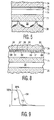
- Fig. 5 illustrates one form of PALC device in accordance with the invention, wherein the thickness of the color filter 70 and/or dielectric sheet 71 are reduced to values within the ranges indicated above, and/or the LC layer thickness 74 is increased to within the range indicated above, and with one or more of the various materials chosen to have the dielectric constants indicated above.
- the fraction of applied voltage Vito actually appearing across each LC pixel can be increased from less than about 1/10 Vito to 0.2 Vito or higher. If we assume that 10V is needed to activate the LC pixel over its full range, it will be appreciated that a column voltage, Vito, of only 20V or less would be required for driving a PALC device according to the invention.
- a LC material with a thickness exceeding 6 ⁇ m can be provided by using a LC material that has a ⁇ n of 0.07 or less, An being the birefringence of the LC material.
- An 0.07
- the product of ⁇ n and the LC layer thickness should equal about 0.48 in order to operate in the first Gooch and Tarry minimum.
- the thickness of the LC layer can be increased to at least about 6.9.
- Examples of such LC materials with a An of 0.07 or less are ZLI 1695 and ZLI 3125 available from the aforesaid E. Merck.
- the LC material chosen should have a dielectric constant at saturation of 4.5 or less. By dielectric constant at saturation is meant the dielectric constant of the material when its transmission is 1%.
- LC materials with this property suitable for use in the invention include MP 88-1068 of E. Merck.
- Fig. 9 shows the typical characteristic curve of transmission vs. voltage for LC materials.
- the significant points, as indicated in Fig. 9, are the voltage at which the transmission falls to 99% and the voltage at which the transmission falls to 1%, referred to herein for convenience as saturation.
- the dielectric constant of the LC material differs at the two points, and the mean dielectric constant usually refers to its average value.
- the dielectric constant at the 1% transmission point is the important value.
- a preferred embodiment of the invention employs a LC material whose dielectric constant at saturation is preferably below 4.5
- another preferred embodiment of the invention employs a LC material whose characteristic curve of transmission vs. voltage falls steeply between the 99% and the 1% transmission points.
- the curve labelled 93 is an example of the steeply-falling characteristic desired for a LC material in accordance with one of the embodiments, which is typical of materials such as ZLI 4801-065 from E. Merck. Such a material has a dielectric constant at saturation of 6.17.
- the dashed curve labelled 94 is typical of an LC material with a low dielectric constant at saturation in accordance with another of the embodiments, such as MP 88-1068 from E.
- Figs. 6A-6M illustrates a preferred method in accordance with the invention for making a color filter 70 having a thickness below about 1 ⁇ m and as low as 0.5 ⁇ m.
- the preferred method involves pigment evaporation onto the substrate previously covered with the ITO electrodes, followed by a liftoff technique.
- Figs. 6A-6M illustrate the process but for simplicity the ITO columns have been omitted.
- a suitable photoresist (PR) adhesion promoter 76 such as silane is applied (Fig. 6A), followed by coating with a thin layer 77 of the PR in the conventional way (Fig. 6B).
- the PR layer is baked and patterned for pigment color 1 (Fig.
- Suitable pigments that when processed as described above will have a thickness below about 1 ⁇ m are: for the blue pigment, Cu-phthalo cyanine, thickness 0.45 ⁇ m; for the red pigment, perylene, thickness 0.38 ⁇ m; for the cyan pigment, Vanadyl-phtalocyanine, and for the yellow pigment, Irgalite yellow, combined thickness of 0.42 ⁇ m.
- the invention is not limited to the particular pigments used in the example given above and any pigments that will provide the basic colors needed to provide a color display, that can be evaporated to produce a layer not exceeding about 1 ⁇ m and/or having a dielectric constant of at least about 5 can be substituted.
- a thin color filter layer with a dielectric constant above about 5 and preferably in the range of 7-9, used alone, will assist in increasing the fraction of Vito applied across the LC layer.
- Another preferred method for achieving a color filter with this property is by using selectively dyed anodized aluminum segments of an evaporated Al film over the ITO-covered substrate.
- Figs. 7A-7F One way of carrying out such a method is illustrated in Figs. 7A-7F.
- a glass substrate 75 (Fig. 7A) is covered with an evaporated ITO film 79 (typical thickness of 150nm) (Fig. 7B), which is then paterned and etched in the usual way to produce the ITO column electrodes 18 (Fig. 7C).
- a thin layer of aluminum is evaporated (typical thickness of about 1000nm) over the ITO electrode columns 18 and patterned and etched in the usual way leaving Al columns 80 in place on top of the ITO columns 18 (Fig.7D).
- every third Al column 80 is selectively anodized to convert same to porous aluminum oxide 81.
- a conventional anodization process can be used, for example, in 15% sulphuric acid, while the intervening two Al columns are masked (not shown) with any suitable masking material (Fig. 7E).
- the subassembly is subjected to a red dye which is absorbed only by the porous anodized regions 81 Fig. 7F).
- the process is then repeated with green and blue dyes, starting from Fig. 7E by selectively anodizing another set of Al columns and dying with a green dye and repeating with a blue dye resulting in the layout shown in Fig. 7G.
- the use of an evaporated film, in this case of aluminum, allows the thickness of the resulting color filter 82 to be kept small, within the range indicated above, and the feature of anodizing it to make selective segments porous allows it to selectively absorb the different dyes needed to reproduce full color and results in a dielectric constant above about 5 and preferably within the range stated above. For this particular example, the dielectric constant will be about 8.5.
- the color filter was provided in the usual way over the ITO column electrodes on the first substrate.
- the color filter layer is provided on the first substrate and then the ITO electrodes deposited on the color filter.
- the anodized aluminum color filter described above is particularly useful in this embodiment because it provides a reasonably firm base for deposition of the ITO electrodes in the normal way by vapor deposition.
- the process described above for the fabrication of the dyed anodyzed aluminum color filter can also be used when the glass substrate is free of the ITO column electrodes. By omitting the color filter from between the ITO electrodes and the plasma channels, none of the applied column voltage is dissipated across the color filter and thus a larger fraction remains effective across the LC pixels.
- This aspect of the invention is not limited to an anodyzed aluminum color filter and other color filter materials which when deposited on the substrate will provide a suitable base for deposition of the ITO electrodes can be substituted.
- Fig. 8 illustrates this embodiment of the invention, and shows the first substrate 34 on which is formed the anodized aluminum segments dyed red 86, green 87, and blue 88, respectively, each covered with an ITO column electrode 89, the spaces between the columns filled with an inert planarizing material 91, and the usual LC layer 74, dielectric sheet 71, and channel substrate 36 provided as previously described.
- the dielectric sheet material to be used in the PALC device of the invention it is preferred to use known glass materials that have a typical dielectric constant of about 6.7 provided in a thickness of at most 40 ⁇ m, preferably about 30 ⁇ m.
- An example of such a glass is a D263 glass from the Schott Company.
- the invention can be used in all kinds of PALC displays that typically have a small channel pitch for use in computer monitors, workstations or TV applications.
- the invention relates to a plasma-addressed liquid crystal color display device comprising a layer of liquid crystal material, data electrodes coupled to the liquid crystal layer and adapted to receive data voltages for activating pixels of the liquid crystal layer, and a plurality of ionizable-gas-filled plasma channels extending generally transverse to the data electrodes for selectively switching on said liquid crystal pixels.
- the plasma channels are sealed off by a thin dielectric sheet, and a color filter layer is provided in the device through which changes in the attenuation of the liquid crystal pixels may be viewed to obtain a color image.
- the device layers are configured and given compositions such that a much higher fraction of the applied data voltages appears across the liquid crystal layer thereby allowing a smaller data voltage to be used to obtain the same effect on the liquid crystal pixels.
- Another feature of the invention includes location of the color filter between the substrate supporting the column electrodes and the column electrodes. Still a further feature is a color filter made up of dyed porous segments of an anodized aluminum film, or of evaporated pigment segments.
Landscapes
- Physics & Mathematics (AREA)
- Engineering & Computer Science (AREA)
- Chemical & Material Sciences (AREA)
- Crystallography & Structural Chemistry (AREA)
- Plasma & Fusion (AREA)
- Nonlinear Science (AREA)
- General Physics & Mathematics (AREA)
- Mathematical Physics (AREA)
- Optics & Photonics (AREA)
- Theoretical Computer Science (AREA)
- Devices For Indicating Variable Information By Combining Individual Elements (AREA)
- Liquid Crystal (AREA)
Claims (8)
- Plasmaadressierte Flüssigkristallwiedergabeanordnung mit einer Schicht aus einem Flüssigkristallmaterial (42), mit Datenelektroden (18) nahe bei einem ersten Substrat (34), wobei diese Elektroden mit der Flüssigkristallschicht gekoppelt sind und Datenspannungen empfangen zur Aktivierung von Teilen der Flüssigkristallschicht, wobei eine Anzahl länglicher Plasmakanäle (20) sich im Allgemeinen quer zu den Datenelektroden (18) erstrecken zur selektiven Einschalten der genannten Flüssigkristallteile, wobei die Flüssigkristallschicht zwischen den Datenelektroden und dem Plasmakanal vorgesehen ist, wobei eine dielektrische Platte (45) die Plasmakanäle an der Seite abschließt, die den Datenelektroden zugewandt ist, und mit einem Farbfilter (56, 70, 82), das der Flüssigkristallschicht zugeordnet ist, wobei die genannten Plasmakanäle (20) je in einem Abstand voneinander liegende längliche Kathoden- und Anoden-Plasma-Elektroden (30, 31) und eine ionisierbare Gasfüllung aufweisen, dadurch gekennzeichnet, dass die Anordnung den Teil der zugeführten Datenspannung an den Flüssigkristallschichtteilen steigert, wenn wenigstens eine der nachfolgenden Bedingungen erfüllt wird:a) die Dicke der Flüssigkristallschicht (42) ist größer als etwa 6 µm,b) das Farbfilter hat eine Dicke unterhalb etwa 3 µm und eine Dielektrizitätskonstante über etwa 5.
- Anordnung nach Anspruch 1, dadurch gekennzeichnet, dass die Dicke der dielektrischen Platte (45) unter etwa 40 µm liegt.
- Anordnung nach Anspruch 1 oder 2, dadurch gekennzeichnet, dass die Dielektrizitätskonstante des Flüssigkristallmaterials (42) unterhalb 4 ist.
- Anordnung nach einem der Ansprüche 1 bis 3, dadurch gekennzeichnet, dass das Farbfilter zwischen dem ersten Substrat (34) und den Datenelektroden (18, 89) vorgesehen ist.
- Anordnung nach einem der Ansprüche 1 bis 3, dadurch gekennzeichnet, dass das Farbfilter (56, 70) zwischen den Datenelektroden (18) und den Plasmakanälen (20) liegt und eine Dielektrizitätskonstante von wenigstens 5 hat und eine Dicke von höchstens etwa 3 µm.
- Anordnung nach einem der Ansprüche 1 bis 5, dadurch gekennzeichnet, dass das Farbfilter poröse Farbsegmente (81) aufweist.
- Anordnung nach Anspruch 6, dadurch gekennzeichnet, dass das Farbfilter einen dünnen Film aus porösem eloxiertem Aluminium aufweist mit nebeneinander liegenden porösen Segmenten (86, 87, 88) gefüllt mit einem von zwei oder mehreren Farbstoffen, die, wenn kombiniert, ein Farbbild erzeugen können.
- Anordnung nach einem der Ansprüche 1 bis 5, dadurch gekennzeichnet, dass das Farbfilter (70) einen dünnen Film aus nebeneinander liegenden aufgedampften Pigmenten aufweist, vorgesehen in einem zyklischen Muster vieler Farben, die, wenn einem Licht ausgesetzt, ein Farbbild erzeugen können.
Applications Claiming Priority (3)
| Application Number | Priority Date | Filing Date | Title |
|---|---|---|---|
| US361087 | 1994-12-21 | ||
| US08/361,087 US5835167A (en) | 1994-12-21 | 1994-12-21 | Plasma addressed liquid crystal display with reduced column voltages |
| PCT/IB1995/001090 WO1996019789A1 (en) | 1994-12-21 | 1995-12-04 | Plasma-addressed liquid crystal display with reduced column voltages |
Publications (2)
| Publication Number | Publication Date |
|---|---|
| EP0746835A1 EP0746835A1 (de) | 1996-12-11 |
| EP0746835B1 true EP0746835B1 (de) | 1999-08-18 |
Family
ID=23420596
Family Applications (1)
| Application Number | Title | Priority Date | Filing Date |
|---|---|---|---|
| EP95937993A Expired - Lifetime EP0746835B1 (de) | 1994-12-21 | 1995-12-04 | Plasmaadressierbare flüssigkristallanzeigevorrichtung mit reduzierten spaltenspannungen |
Country Status (6)
| Country | Link |
|---|---|
| US (1) | US5835167A (de) |
| EP (1) | EP0746835B1 (de) |
| JP (1) | JPH09509761A (de) |
| KR (1) | KR970701406A (de) |
| DE (1) | DE69511527T2 (de) |
| WO (1) | WO1996019789A1 (de) |
Families Citing this family (9)
| Publication number | Priority date | Publication date | Assignee | Title |
|---|---|---|---|---|
| US5994721A (en) * | 1995-06-06 | 1999-11-30 | Ois Optical Imaging Systems, Inc. | High aperture LCD with insulating color filters overlapping bus lines on active substrate |
| EP0830666B1 (de) * | 1996-03-18 | 2000-05-10 | Koninklijke Philips Electronics N.V. | Plasmaadressierte anzeigevorrichtung |
| US5909260A (en) * | 1996-05-24 | 1999-06-01 | Tektronix, Inc. | Plasma addressed liquid crystal display panel with reduced data drive electrode capacitance |
| EP0818703A3 (de) * | 1996-07-12 | 1998-02-11 | Tektronix, Inc. | Plasmaadressierte Flüssigkristallanzeigetafel mit optimiertem Verhältnis zwischen den Flüssigkristallparametern und der Abdeckplattendicke |
| EP0818799A3 (de) * | 1996-07-12 | 1998-09-23 | Tektronix, Inc. | Kathodenstruktur für eine plasmaadressierte Flüssigkristallanzeigetafel |
| US6137550A (en) * | 1996-09-30 | 2000-10-24 | Tektronix, Inc. | Structure for a PALC display panel having a helium filling doped with hydrogen |
| KR19990076932A (ko) * | 1996-10-25 | 1999-10-25 | 요트.게.아. 롤페즈 | 감소된 컬럼 전압을 갖춘 플라즈마 어드레스된액정 디스플레이 장치 |
| US7146441B1 (en) | 1998-03-16 | 2006-12-05 | Actel Corporation | SRAM bus architecture and interconnect to an FPGA |
| JP3479023B2 (ja) | 1999-05-18 | 2003-12-15 | シャープ株式会社 | 電気配線の製造方法および配線基板および表示装置および画像検出器 |
Family Cites Families (16)
| Publication number | Priority date | Publication date | Assignee | Title |
|---|---|---|---|---|
| EP0112695B1 (de) * | 1982-12-22 | 1987-08-12 | Seiko Instruments Inc. | Verfahren zur Herstellung eines mehrfach gefärbten Bauteiles |
| JPS60254001A (ja) * | 1984-05-14 | 1985-12-14 | Nissha Printing Co Ltd | カラ−フイルタ− |
| US5305154A (en) * | 1987-01-28 | 1994-04-19 | Nissha Printing Co., Ltd. | Color filter with a porous activated film layer having dyes fixed in the minute pores to form a color pattern |
| KR960013793B1 (ko) * | 1987-01-28 | 1996-10-10 | 니혼샤신인사츠 가부시키가이샤 | 컬러필터의 제조방법 |
| US5077553A (en) * | 1988-01-19 | 1991-12-31 | Tektronix, Inc. | Apparatus for and methods of addressing data storage elements |
| US5272472A (en) * | 1988-01-19 | 1993-12-21 | Tektronix, Inc. | Apparatus for addressing data storage elements with an ionizable gas excited by an AC energy source |
| US4896149A (en) * | 1988-01-19 | 1990-01-23 | Tektronix, Inc. | Addressing structure using ionizable gaseous medium |
| JP2700945B2 (ja) * | 1990-08-30 | 1998-01-21 | キヤノン株式会社 | カラーフィルター付き基板 |
| JPH04265936A (ja) * | 1991-02-20 | 1992-09-22 | Sony Corp | 画像表示装置の製造方法 |
| JP3173061B2 (ja) * | 1991-09-11 | 2001-06-04 | ソニー株式会社 | プラズマアドレス電気光学装置 |
| US5519520A (en) * | 1992-02-24 | 1996-05-21 | Photonics Systems, Inc. | AC plasma address liquid crystal display |
| JP3185353B2 (ja) * | 1992-04-21 | 2001-07-09 | ソニー株式会社 | プラズマアドレス電気光学装置 |
| US5276384A (en) * | 1992-08-26 | 1994-01-04 | Tektronix, Inc. | Electrode configuration for channel confinement of plasma discharge in an electrode structure using an ionizable gaseous medium |
| JP2847666B2 (ja) * | 1993-03-04 | 1999-01-20 | テクトロニクス・インコーポレイテッド | 電気光学表示方法 |
| US5461395A (en) * | 1993-03-08 | 1995-10-24 | Tektronix, Inc. | Plasma addressing structure having a pliant dielectric layer |
| JPH06317785A (ja) * | 1993-05-07 | 1994-11-15 | Sony Corp | プラズマアドレス液晶表示装置 |
-
1994
- 1994-12-21 US US08/361,087 patent/US5835167A/en not_active Expired - Fee Related
-
1995
- 1995-12-04 WO PCT/IB1995/001090 patent/WO1996019789A1/en not_active Ceased
- 1995-12-04 KR KR1019960704657A patent/KR970701406A/ko not_active Abandoned
- 1995-12-04 JP JP8519635A patent/JPH09509761A/ja not_active Abandoned
- 1995-12-04 DE DE69511527T patent/DE69511527T2/de not_active Expired - Fee Related
- 1995-12-04 EP EP95937993A patent/EP0746835B1/de not_active Expired - Lifetime
Also Published As
| Publication number | Publication date |
|---|---|
| DE69511527D1 (de) | 1999-09-23 |
| KR970701406A (ko) | 1997-03-17 |
| WO1996019789A1 (en) | 1996-06-27 |
| US5835167A (en) | 1998-11-10 |
| JPH09509761A (ja) | 1997-09-30 |
| DE69511527T2 (de) | 2000-02-17 |
| EP0746835A1 (de) | 1996-12-11 |
Similar Documents
| Publication | Publication Date | Title |
|---|---|---|
| US5808413A (en) | Plasma addressed liquid crystal display with organic-walled plasma channels | |
| US5804920A (en) | Plasma addressed liquid crystal display with etched glass spacers | |
| US5835167A (en) | Plasma addressed liquid crystal display with reduced column voltages | |
| US5868811A (en) | Method of making a channel plate for a flat display device | |
| US6130655A (en) | Plasma-addressed display | |
| US5596431A (en) | Plasma addressed liquid crystal display with etched electrodes | |
| US6579462B2 (en) | Plasma addressed liquid crystal display with glass spacers | |
| EP0760992B1 (de) | Plasmagesteuerte flüssigkristallanzeige mit geätztem plasmakanälen | |
| EP0746836B1 (de) | Kanalanordnung für plasmagesteuerte flüssigkristallanzeigevorrichtung | |
| EP0827617B1 (de) | Plasma-adressierte farbanzeigevorrichtung | |
| US6064153A (en) | Channel subassembly for a plasma addressed liquid crystal display panel | |
| US6233028B1 (en) | Plasma-addressed liquid crystal display with reduced column voltages | |
| JPH0752266B2 (ja) | 反射型液晶表示デバイス | |
| US6057895A (en) | Plasmas addressed liquid crystal display with deposited plasma channels with tapered edges | |
| US5903325A (en) | Plasma addressed liquid crystal display panel with optimized relationship between liquid crystal parameters and cover sheet thickness |
Legal Events
| Date | Code | Title | Description |
|---|---|---|---|
| PUAI | Public reference made under article 153(3) epc to a published international application that has entered the european phase |
Free format text: ORIGINAL CODE: 0009012 |
|
| AK | Designated contracting states |
Kind code of ref document: A1 Designated state(s): DE FR GB NL |
|
| 17P | Request for examination filed |
Effective date: 19961227 |
|
| 17Q | First examination report despatched |
Effective date: 19980130 |
|
| GRAG | Despatch of communication of intention to grant |
Free format text: ORIGINAL CODE: EPIDOS AGRA |
|
| GRAG | Despatch of communication of intention to grant |
Free format text: ORIGINAL CODE: EPIDOS AGRA |
|
| GRAH | Despatch of communication of intention to grant a patent |
Free format text: ORIGINAL CODE: EPIDOS IGRA |
|
| GRAG | Despatch of communication of intention to grant |
Free format text: ORIGINAL CODE: EPIDOS AGRA |
|
| GRAH | Despatch of communication of intention to grant a patent |
Free format text: ORIGINAL CODE: EPIDOS IGRA |
|
| GRAA | (expected) grant |
Free format text: ORIGINAL CODE: 0009210 |
|
| AK | Designated contracting states |
Kind code of ref document: B1 Designated state(s): DE FR GB NL |
|
| PG25 | Lapsed in a contracting state [announced via postgrant information from national office to epo] |
Ref country code: NL Free format text: LAPSE BECAUSE OF FAILURE TO SUBMIT A TRANSLATION OF THE DESCRIPTION OR TO PAY THE FEE WITHIN THE PRESCRIBED TIME-LIMIT Effective date: 19990818 |
|
| REF | Corresponds to: |
Ref document number: 69511527 Country of ref document: DE Date of ref document: 19990923 |
|
| ET | Fr: translation filed | ||
| NLV1 | Nl: lapsed or annulled due to failure to fulfill the requirements of art. 29p and 29m of the patents act | ||
| PLBE | No opposition filed within time limit |
Free format text: ORIGINAL CODE: 0009261 |
|
| STAA | Information on the status of an ep patent application or granted ep patent |
Free format text: STATUS: NO OPPOSITION FILED WITHIN TIME LIMIT |
|
| 26N | No opposition filed | ||
| REG | Reference to a national code |
Ref country code: GB Ref legal event code: IF02 |
|
| REG | Reference to a national code |
Ref country code: GB Ref legal event code: 746 Effective date: 20020918 |
|
| REG | Reference to a national code |
Ref country code: FR Ref legal event code: D6 |
|
| PGFP | Annual fee paid to national office [announced via postgrant information from national office to epo] |
Ref country code: DE Payment date: 20030217 Year of fee payment: 8 |
|
| PGFP | Annual fee paid to national office [announced via postgrant information from national office to epo] |
Ref country code: GB Payment date: 20031224 Year of fee payment: 9 |
|
| PGFP | Annual fee paid to national office [announced via postgrant information from national office to epo] |
Ref country code: FR Payment date: 20031229 Year of fee payment: 9 |
|
| PG25 | Lapsed in a contracting state [announced via postgrant information from national office to epo] |
Ref country code: DE Free format text: LAPSE BECAUSE OF NON-PAYMENT OF DUE FEES Effective date: 20040701 |
|
| PG25 | Lapsed in a contracting state [announced via postgrant information from national office to epo] |
Ref country code: GB Free format text: LAPSE BECAUSE OF NON-PAYMENT OF DUE FEES Effective date: 20041204 |
|
| GBPC | Gb: european patent ceased through non-payment of renewal fee |
Effective date: 20041204 |
|
| PG25 | Lapsed in a contracting state [announced via postgrant information from national office to epo] |
Ref country code: FR Free format text: LAPSE BECAUSE OF NON-PAYMENT OF DUE FEES Effective date: 20050831 |
|
| REG | Reference to a national code |
Ref country code: FR Ref legal event code: ST |