EP0744774A2 - Field effect transistor and method for producing same - Google Patents
Field effect transistor and method for producing same Download PDFInfo
- Publication number
- EP0744774A2 EP0744774A2 EP96108283A EP96108283A EP0744774A2 EP 0744774 A2 EP0744774 A2 EP 0744774A2 EP 96108283 A EP96108283 A EP 96108283A EP 96108283 A EP96108283 A EP 96108283A EP 0744774 A2 EP0744774 A2 EP 0744774A2
- Authority
- EP
- European Patent Office
- Prior art keywords
- active layer
- heavily doped
- layer
- field effect
- effect transistor
- Prior art date
- Legal status (The legal status is an assumption and is not a legal conclusion. Google has not performed a legal analysis and makes no representation as to the accuracy of the status listed.)
- Withdrawn
Links
- 230000005669 field effect Effects 0.000 title claims abstract description 90
- 238000004519 manufacturing process Methods 0.000 title claims description 22
- 239000004065 semiconductor Substances 0.000 claims abstract description 65
- 239000012535 impurity Substances 0.000 claims abstract description 55
- 239000000758 substrate Substances 0.000 claims abstract description 54
- 230000015572 biosynthetic process Effects 0.000 claims description 24
- 230000015556 catabolic process Effects 0.000 description 33
- VYPSYNLAJGMNEJ-UHFFFAOYSA-N Silicium dioxide Chemical compound O=[Si]=O VYPSYNLAJGMNEJ-UHFFFAOYSA-N 0.000 description 16
- 230000005684 electric field Effects 0.000 description 16
- 229920002120 photoresistant polymer Polymers 0.000 description 14
- JBRZTFJDHDCESZ-UHFFFAOYSA-N AsGa Chemical compound [As]#[Ga] JBRZTFJDHDCESZ-UHFFFAOYSA-N 0.000 description 12
- 229910001218 Gallium arsenide Inorganic materials 0.000 description 11
- 238000000034 method Methods 0.000 description 10
- 229910052681 coesite Inorganic materials 0.000 description 8
- 229910052906 cristobalite Inorganic materials 0.000 description 8
- 230000003071 parasitic effect Effects 0.000 description 8
- 239000000377 silicon dioxide Substances 0.000 description 8
- 229910052682 stishovite Inorganic materials 0.000 description 8
- 229910052905 tridymite Inorganic materials 0.000 description 8
- 150000002500 ions Chemical class 0.000 description 7
- 230000008569 process Effects 0.000 description 7
- 238000005468 ion implantation Methods 0.000 description 6
- 150000001875 compounds Chemical class 0.000 description 5
- 230000000694 effects Effects 0.000 description 5
- 229910017401 Au—Ge Inorganic materials 0.000 description 2
- NBIIXXVUZAFLBC-UHFFFAOYSA-N Phosphoric acid Chemical compound OP(O)(O)=O NBIIXXVUZAFLBC-UHFFFAOYSA-N 0.000 description 2
- 238000009826 distribution Methods 0.000 description 2
- 238000012986 modification Methods 0.000 description 2
- 230000004048 modification Effects 0.000 description 2
- 230000009467 reduction Effects 0.000 description 2
- 229920005989 resin Polymers 0.000 description 2
- 239000011347 resin Substances 0.000 description 2
- 238000001771 vacuum deposition Methods 0.000 description 2
- 229910052782 aluminium Inorganic materials 0.000 description 1
- XAGFODPZIPBFFR-UHFFFAOYSA-N aluminium Chemical compound [Al] XAGFODPZIPBFFR-UHFFFAOYSA-N 0.000 description 1
- 229910000147 aluminium phosphate Inorganic materials 0.000 description 1
- 239000007864 aqueous solution Substances 0.000 description 1
- 230000000052 comparative effect Effects 0.000 description 1
- 239000013078 crystal Substances 0.000 description 1
- 230000002542 deteriorative effect Effects 0.000 description 1
- 229920001971 elastomer Polymers 0.000 description 1
- 238000005538 encapsulation Methods 0.000 description 1
- 238000010438 heat treatment Methods 0.000 description 1
- 238000002513 implantation Methods 0.000 description 1
- 239000007788 liquid Substances 0.000 description 1
- 239000000463 material Substances 0.000 description 1
- 229920003986 novolac Polymers 0.000 description 1
- 238000012545 processing Methods 0.000 description 1
- 238000012827 research and development Methods 0.000 description 1
- 238000001039 wet etching Methods 0.000 description 1
Images


Classifications
-
- H—ELECTRICITY
- H01—ELECTRIC ELEMENTS
- H01L—SEMICONDUCTOR DEVICES NOT COVERED BY CLASS H10
- H01L29/00—Semiconductor devices adapted for rectifying, amplifying, oscillating or switching, or capacitors or resistors with at least one potential-jump barrier or surface barrier, e.g. PN junction depletion layer or carrier concentration layer; Details of semiconductor bodies or of electrodes thereof ; Multistep manufacturing processes therefor
- H01L29/66—Types of semiconductor device ; Multistep manufacturing processes therefor
- H01L29/66007—Multistep manufacturing processes
- H01L29/66075—Multistep manufacturing processes of devices having semiconductor bodies comprising group 14 or group 13/15 materials
- H01L29/66227—Multistep manufacturing processes of devices having semiconductor bodies comprising group 14 or group 13/15 materials the devices being controllable only by the electric current supplied or the electric potential applied, to an electrode which does not carry the current to be rectified, amplified or switched, e.g. three-terminal devices
- H01L29/66409—Unipolar field-effect transistors
- H01L29/66848—Unipolar field-effect transistors with a Schottky gate, i.e. MESFET
- H01L29/66856—Unipolar field-effect transistors with a Schottky gate, i.e. MESFET with an active layer made of a group 13/15 material
- H01L29/66863—Lateral single gate transistors
-
- H—ELECTRICITY
- H01—ELECTRIC ELEMENTS
- H01L—SEMICONDUCTOR DEVICES NOT COVERED BY CLASS H10
- H01L29/00—Semiconductor devices adapted for rectifying, amplifying, oscillating or switching, or capacitors or resistors with at least one potential-jump barrier or surface barrier, e.g. PN junction depletion layer or carrier concentration layer; Details of semiconductor bodies or of electrodes thereof ; Multistep manufacturing processes therefor
- H01L29/66—Types of semiconductor device ; Multistep manufacturing processes therefor
- H01L29/68—Types of semiconductor device ; Multistep manufacturing processes therefor controllable by only the electric current supplied, or only the electric potential applied, to an electrode which does not carry the current to be rectified, amplified or switched
- H01L29/76—Unipolar devices, e.g. field effect transistors
- H01L29/772—Field effect transistors
-
- H—ELECTRICITY
- H01—ELECTRIC ELEMENTS
- H01L—SEMICONDUCTOR DEVICES NOT COVERED BY CLASS H10
- H01L29/00—Semiconductor devices adapted for rectifying, amplifying, oscillating or switching, or capacitors or resistors with at least one potential-jump barrier or surface barrier, e.g. PN junction depletion layer or carrier concentration layer; Details of semiconductor bodies or of electrodes thereof ; Multistep manufacturing processes therefor
- H01L29/02—Semiconductor bodies ; Multistep manufacturing processes therefor
- H01L29/06—Semiconductor bodies ; Multistep manufacturing processes therefor characterised by their shape; characterised by the shapes, relative sizes, or dispositions of the semiconductor regions ; characterised by the concentration or distribution of impurities within semiconductor regions
- H01L29/08—Semiconductor bodies ; Multistep manufacturing processes therefor characterised by their shape; characterised by the shapes, relative sizes, or dispositions of the semiconductor regions ; characterised by the concentration or distribution of impurities within semiconductor regions with semiconductor regions connected to an electrode carrying current to be rectified, amplified or switched and such electrode being part of a semiconductor device which comprises three or more electrodes
- H01L29/0843—Source or drain regions of field-effect devices
- H01L29/0891—Source or drain regions of field-effect devices of field-effect transistors with Schottky gate
-
- H—ELECTRICITY
- H01—ELECTRIC ELEMENTS
- H01L—SEMICONDUCTOR DEVICES NOT COVERED BY CLASS H10
- H01L29/00—Semiconductor devices adapted for rectifying, amplifying, oscillating or switching, or capacitors or resistors with at least one potential-jump barrier or surface barrier, e.g. PN junction depletion layer or carrier concentration layer; Details of semiconductor bodies or of electrodes thereof ; Multistep manufacturing processes therefor
- H01L29/40—Electrodes ; Multistep manufacturing processes therefor
- H01L29/41—Electrodes ; Multistep manufacturing processes therefor characterised by their shape, relative sizes or dispositions
- H01L29/417—Electrodes ; Multistep manufacturing processes therefor characterised by their shape, relative sizes or dispositions carrying the current to be rectified, amplified or switched
- H01L29/41725—Source or drain electrodes for field effect devices
- H01L29/41775—Source or drain electrodes for field effect devices characterised by the proximity or the relative position of the source or drain electrode and the gate electrode, e.g. the source or drain electrode separated from the gate electrode by side-walls or spreading around or above the gate electrode
-
- H—ELECTRICITY
- H01—ELECTRIC ELEMENTS
- H01L—SEMICONDUCTOR DEVICES NOT COVERED BY CLASS H10
- H01L29/00—Semiconductor devices adapted for rectifying, amplifying, oscillating or switching, or capacitors or resistors with at least one potential-jump barrier or surface barrier, e.g. PN junction depletion layer or carrier concentration layer; Details of semiconductor bodies or of electrodes thereof ; Multistep manufacturing processes therefor
- H01L29/66—Types of semiconductor device ; Multistep manufacturing processes therefor
- H01L29/68—Types of semiconductor device ; Multistep manufacturing processes therefor controllable by only the electric current supplied, or only the electric potential applied, to an electrode which does not carry the current to be rectified, amplified or switched
- H01L29/76—Unipolar devices, e.g. field effect transistors
- H01L29/772—Field effect transistors
- H01L29/80—Field effect transistors with field effect produced by a PN or other rectifying junction gate, i.e. potential-jump barrier
- H01L29/812—Field effect transistors with field effect produced by a PN or other rectifying junction gate, i.e. potential-jump barrier with a Schottky gate
- H01L29/8128—Field effect transistors with field effect produced by a PN or other rectifying junction gate, i.e. potential-jump barrier with a Schottky gate with recessed gate
Landscapes
- Engineering & Computer Science (AREA)
- Microelectronics & Electronic Packaging (AREA)
- Power Engineering (AREA)
- Physics & Mathematics (AREA)
- Ceramic Engineering (AREA)
- Condensed Matter Physics & Semiconductors (AREA)
- General Physics & Mathematics (AREA)
- Computer Hardware Design (AREA)
- Manufacturing & Machinery (AREA)
- Junction Field-Effect Transistors (AREA)
Abstract
Description
- The present invention relates to a field effect transistor and a method of manufacturing the same, and more particularly to a compound semiconductor field effect transistor for use as a high frequency device or a high power device and a method for producing the same.
- In general, the mobility of electrons in a low electrical field is higher in a compound semiconductor than in Si. This means that the speed of electrons moving in a compound semiconductor can be higher than in Si. Therefore, a compound semiconductor is suitable for microwave and millimeter-wave devices and high power devices. Especially, field effect transistors having a Schottky junction gate utilizing gallium arsenide (GaAs), which is a typical material for compound semiconductors (hereinafter referred to as a "GaAs MESFET"), are under active research and development for realizing a low noise, high power device for use as a microwave device.
- A GaAs MESFET is generally configured by forming a gate electrode in Schottky contact with an active layer formed on the upper surface of a semi-insulating GaAs substrate and by forming a source electrode and a drain electrode in ohmic contact with the active layer on both sides of the gate electrode. However, a surface depletion layer is generated by surface charge on the surface of the GaAs substrate, which above-described configuration is unable to provide excellent increases parasitic resistance and reduces both mutual conductance gm in high frequency bands and a current gain cut-off frequency fT. Therefore, a GaAs MESFET having the high frequency characteristics and is limited in applicability to high power use.
- In order to avoid the influence of a surface depletion layer, there has been conceived a recessed gate structure in which a recess is formed in a active layer and a gate electrode is formed on the bottom of the recess. In a recessed gate structure, the recess improves high frequency characteristics, and the breakdown voltage can be increased by preventing an electrical field from concentrating at an edge of the gate electrode. Moreover, a heavily doped layer having a high impurity concentration is formed at the areas where the drain and source electrodes are to be formed in order to reduce the ohmic contact resistance between the drain and source electrodes and the active layer.
- Further, in order to improve the breakdown characteristics such as the gate breakdown voltage, there has been conceived an offset gate structure in which a distance between the gate electrode and the drain electrode is greater than that between the gate electrode and source electrode to prevent an electric field from concentrating at an edge of the gate electrode on the side toward the drain electrode. There has also been conceived a step recess structure in which a recess is formed at the bottom of another recess to formed stepped side faces.
- In addition, an LDD (Lightly Doped Drain) structure as shown in Fig. 13 has recently been proposed. The field effect transistor having the LDD structure shown in Fig. 13 is configured by forming a
source electrode 102, adrain electrode 103, and agate electrode 101 on the upper surface of aGaAs substrate 110 having anactive layer 111, heavily dopedlayers 112 and 113, and a moderately (medium) dopedlayer 114. In the field effect transistor having the LDD structure shown in Fig. 13, the impurity concentration of the moderately dopedlayer 114 is set to a value in the range between the impurity concentrations of theactive layer 111 and the heavily dopedlayers 112 and 113. According to the structure, the gate breakdown voltage is increased by relieving a electrical field at the edge of thegate electrode 101 on the side toward thedrain electrode 103. - However, the above-described offset gate structure has a problem in that the great distance between the gate and drain electrodes increases parasitic resistance between the gate and drain electrodes, thereby deteriorating high frequency characteristics. Further, although the offset gate structure, step recess structure, and LDD structure can improve the gate breakdown voltage by relieving an electrical field at the edge of the gate electrode, drain breakdown voltage cannot be improved. This has resulted in a problem in that an FET having such a structure is difficult to use at high power.
- In order to obtain a sufficient drain breakdown voltage, given these considerations, the distance between the gate and drain electrodes must be large as in an offset gate structure, and this increases parasitic resistance. This has also resulted in a problem, in that the mutual conductance gm in high frequency bands and current gain cut-off frequency fT cannot be increased. Furthermore, the above-described step recess structure and LDD structure have had a problem, in that they involve complicated manufacturing processes which make control over processing conditions difficult and in that a GaAs MESFET having the above-described step recess structure and a GaAs MESFET having the LDD structure are not reliable enough.
- It is therefore an object of the preferred embodiments of present invention to provide a field effect transistor and a method of manufacturing the same in which the above-described problems are solved and in which the mutual inductance gm in high frequency bands and the current gain cut-off frequency fT can be high.
- According to a preferred embodiment of the invention, a field effect transistor includes: a semiconductor substrate; an active layer formed on a part of a principal surface of the semiconductor substrate and having a predetermined impurity concentration; first and second heavily doped layers having an impurity concentration higher than the impurity concentration of the active layer formed in two respective areas of the principal surface of the semiconductor substrate located on both sides of the active layer in contact with the active layer; a gate electrode formed on a surface of the active layer; a drain electrode formed on a surface of the first heavily doped layer; and a source electrode formed on the surface of the second heavily doped layer, wherein at least one of the drain electrode and the source electrode is formed so as to extend onto a surface of the active layer.
- According to another preferred embodiment of the present invention, a field effect transistor includes: a semiconductor substrate; an active layer formed on a part of a principal surface of the semiconductor substrate and having a predetermined impurity concentration; first and second heavily doped layers having an impurity concentration higher than the impurity concentration of the active layer formed in two respective areas of the principal surface of the semiconductor substrate and located on both sides of the active layer at predetermined intervals from the active layer; medium doped layers having an impurity concentration higher than the impurity concentration of the active layer and lower than the impurity concentration of the heavily doped layers formed in a region between the active layer and the first heavily doped layer and a region between the active layer and the second heavily doped layer; a gate electrode formed on a surface of the active layer; a drain electrode formed on the surface of the first heavily doped layer; and a source electrode formed on a surface of the second heavily doped layer, wherein at least one of the drain electrode and said source electrode is formed so as to extend onto a surface of said medium doped layer.
- In a further embodiment, both of said drain electrode and said source electrode are formed so as to extend onto a surface of the medium doped layer or the active layer.
- In another embodiment, a recess is formed by removing said active layer from the surface thereof to a predetermined depth, and the gate electrode is formed on the bottom of the recess.
- In yet another embodiment, a step portion is formed in at least one of said first and second heavily doped layers, and the drain electrode or source electrode is formed on said step portion.
- According to still another aspect of the invention, a method of manufacturing a field effect transistor includes the steps of: forming an active layer having a predetermined impurity density on a part of a principal surface of a semiconductor substrate; forming first and second heavily doped layers having an impurity density higher than the impurity density of the active layer in two respective areas of the principal surface of the semiconductor substrate located on both sides of the active layer and in contact with the active layer; forming a resist film on the principal surface of the semiconductor substrate so as to expose a drain electrode formation region including a surface of the first heavily doped layer and a source electrode formation region including a surface of the second heavily doped layer, at least one of the drain electrode formation region and the source electrode formation region also including a part of the surface of the active layer including either the part in contact with the first heavily doped layer or the second heavily doped layer; forming a drain electrode in the drain electrode formation region and forming a source electrode in the source electrode formation region; removing the resist film; and forming a gate electrode on the surface of the active layer located between the drain electrode and the source electrode at a predetermined interval from each of the drain electrode and the source electrode.
- According to the field effect transistor of the preferred embodiments, the source electrode or the drain electrode provided on the heavily doped layer is in contact with the active layer or the medium doped layer at the end portion thereof. Therefore, a voltage drop of the voltage across the gate electrode and either the source electrode or the drain electrode is greater at the end portion than at the other portion of the electrode. As a result, an electrical field in the active layer in the vicinity of the end portion is relieved, and the drain breakdown voltage or source breakdown voltage can be improved. Further, since the source-gate distance and the drain-gate distance can be reduced, the gate-drain parasitic resistance and the gate-source parasitic resistance can be reduced. As a result, the mutual conductance gm in high frequency bands can be increased and a current gain cut-off frequency fT can be made higher. The maximum output can be also increased.
- For the purpose of illustrating the invention, there are shown in the drawings several forms which are presently preferred, it being understood, however, that the invention is not limited to the precise arrangements and instrumentalities shown. Other features and advantages or the present invention will become apparent from the following description.
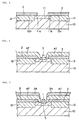
- Fig. 1 is a sectional view of a field effect transistor of a first embodiment of the present invention.
- Fig. 2 is a sectional view of a
semiconductor substrate 10 on the upper surface of which an n-type semiconductor layer 31 is formed in a step of manufacturing the field effect transistor of the embodiment shown in Fig. 1. - Fig. 3 is a sectional view of the
semiconductor substrate 10 on which heavily dopedlayers - Fig. 4 is a sectional view of the
semiconductor substrate 10 on which aresist film 46 is formed in a step of manufacturing the field effect transistor of the embodiment shown in Fig. 1. - Fig. 5 is a sectional view of the
semiconductor substrate 10 on which a source electrode and a drain electrode are formed in a step of manufacturing the field effect transistor of the embodiment shown in Fig. 1. - Fig. 6 is a sectional view of the
semiconductor substrate 10 on which aresist film 47 is formed in a step of manufacturing the field effect transistor of the embodiment shown in Fig. 1. - Fig. 7 is a sectional view of the
semiconductor substrate 10 on which anelectrode 1 is formed in a step of manufacturing the field effect transistor of the embodiment shown in Fig. 1. - Fig. 8 is a sectional view of a
field effect transistor 22 of a second embodiment of the present invention. - Fig. 9 is a sectional view of the
semiconductor substrate 10 on which ion implantation is carried out after forming a SiO2 film 48 in a step of manufacturing thefield effect transistor 22 of the second embodiment. - Fig. 10 is a sectional view of the
semiconductor substrate 10 on which ion implantation is carried out after formingside walls 49a and 49b on the sides of the SiO2 film 48 in a step of manufacturing thefield effect transistor 22 of the second embodiment. - Fig. 11 is a sectional view of a
field effect transistor 23 of a third embodiment of the present invention. - Fig. 12 is a sectional view of a
field effect transistor 24 of a fourth embodiment of the present invention. - Fig. 13 is a sectional view of a conventional field effect transistor.
- Hereinafter, preferred embodiments of the present invention are explained in detail with reference to the drawings.
- Fig. 1 is a sectional view of a
field effect transistor 21 according to a first embodiment of the present invention. Thefield effect transistor 21 is a gallium arsenide MESFET and includes asemiconductor substrate 10. Anactive layer 11 is provided on thesemiconductor substrate 10 and heavily dopedlayers semiconductor substrate 10 on respective sides of theactive layer 11. Arecess 5 is provided in theactive layer 11 and agate electrode 1 is provided on the bottom of therecess 5. - A
source electrode 2 is provided on asurface 12a of the heavily dopedlayer 12 and a surface 11a of theactive layer 11, while adrain electrode 3 is provided on asurface 13a of the heavily dopedlayer 13 and asurface 11b of theactive layer 11. That is, thesource electrode 2 is provided so as to extend from thesurface 12a of the heavily dopedlayer 12 to the surface 11a of theactive layer 11, and thedrain electrode 3 is formed so as to extend from thesurface 13a of the heavily dopedlayer 13 to thesurface 11b of theactive layer 11. As a result, the edges of thesource electrode 2 and thedrain electrode 3 are offset toward the gate electrode with respect to the edge of the heavily dopedlayers - The configuration of the field effect transistor of the first embodiment will now be described in more detail with reference to Fig. 1. In Fig. 1, the
semiconductor substrate 10 is constituted by GaAs single crystal produced using the liquid encapsulation Czochralski method. The active later 11 is an n-type semiconductor layer having a predetermined width L5 and a predetermined length in a gate length direction and having a predetermined impurity concentration, provided on thesemiconductor substrate 10. Further, a groove-shapedrecess 5 having a predetermined width, a predetermined length, and a predetermined depth extending along the gate width direction is provided in the middle of the surface of theactive layer 11. - The heavily doped
layers semiconductor substrate 10 on both sides of theactive layer 11 so as to be in contact with theactive layer 11. The heavily dopedlayers active layer 11. - The
gate electrode 1 is formed on the bottom of therecess 5 along the extending direction of therecess 5 and is in Schottky contact with theactive layer 11. Thesource electrode 2 and thedrain electrode 3 are formed on both sides of thegate electrode 1 at predetermined intervals from thegate electrode 1. - The
source electrode 2 is formed on thesurface 12a of the heavily dopedlayer 12 and the surface 11a of theactive layer 11, and this forms ohmic contact between thesource electrode 2 and the heavily dopedlayer 12 and ohmic contact between thesource electrode 2 and theactive layer 11. The surface 11a of theactive layer 11 is a portion having a predetermined width L2 along the surface of theactive layer 11 which extends along the boundary between theactive layer 11 and the heavily dopedlayer 12. Thedrain electrode 3 is formed on thesurface 13a of the heavily dopedlayer 13 and thesurface 11b of theactive layer 11, and this forms ohmic contact between thedrain electrode 3 and the heavily dopedlayer 13 and ohmic contact between thedrain electrode 3 and theactive layer 11. Thesurface 11b of theactive layer 11 is a portion having a predetermined width L3 along the surface of theactive layer 11 which extends along the boundary between theactive layer 11 and the heavily dopedlayer 13. - Since the heavily doped
layer 12 has an impurity concentration higher than that of theactive layer 11, contact resistance between the heavily dopedlayer 12 and thesource electrode 2 at thesurface 12a of the heavily dopedlayer 12 is lower than contact resistance between theactive layer 11 and thesource electrode 2 at the surface 11a of theactive layer 11. Similarly, since the heavily dopedlayer 13 has an impurity concentration higher than that of theactive layer 11, contact resistance between the heavily dopedlayer 13 and thedrain electrode 3 at thesurface 13a of the heavily dopedlayer 13 is lower than contact resistance between theactive layer 11 and thedrain electrode 3 at thesurface 11b of theactive layer 11. Thefield effect transistor 21 of the first embodiment is configured as described above. - A method of manufacturing the
field effect transistor 21 will now be described. Figs. 2 through 7 are sectional views of thesemiconductor substrate 10 after major steps of the manufacturing method. The method of manufacturing thefield effect transistor 21 will now be described with reference to the drawings. - According to the method of manufacturing the
field effect transistor 21 of the first embodiment, as shown in Fig. 2, an n-type semiconductor layer 31 is first formed on the upper surface of asemiconductor substrate 10 by implanting impurities which are Si+ ions using an ion implantation process under a condition of 80 KeV, 6X 10¹²/cm2. - Next, as shown in Fig. 3, a photo resist 45 mainly composed of novolac type resin, cyclized rubber type resin or the like is formed in the middle of the
semiconductor substrate 10. The photo resist 45 extends along a direction which to be a gate width direction and has a width of L5 and a predetermined length. Impurities ions such as Si+ ions are implanted using the photo resist 45 as a mask by an ion implantation process from above thesemiconductor substrate 10 under conditions of 120 KeV, 2X 10¹³/cm2 . As a result, anactive layer 11 having an impurity concentration equal to the impurity concentration of the n-type semiconductor layer 31 is remained directly under the photo resist 45, and heavily dopedlayers type semiconductor layer 31 are formed on both sides of theactive layer 11. - Next, as shown in Fig. 4, after removing the photo resist 45, a photo resist 46 extending along the gate width direction is formed in the middle of the surface of the
active layer 11. The photo resist 46 has a width of L4 which is smaller than the width of L5. The photo resist 46 is formed on the surface of theactive layer 11 so that a sourceelectrode formation region 32 including asurface 12a of a heavily dopedlayer 12 and a surface 11a of theactive layer 11 and a drainelectrode formation region 33 including asurface 13a of a heavily dopedregion 13 and asurface 11b of theactive layer 11 are exposed. - Then, Au-Ge/Ni type electrodes are formed using a vacuum deposition process from above the
semiconductor substrate 10. After removing the photo resist 46 by a lift-off method, the Au-Ge/Ni type electrodes are alloyed by performing heat treatment at a temperature of 380°C to form asource electrode 2 in ohmic contact with the heavily dopedlayer 12 and theactive layer 11 and adrain electrode 3 in ohmic contact with the heavily dopedlayer 13 and theactive layer 11. Thus, as shown in Fig. 5, thesource electrode 2 is formed on thesurface 12a of the heavily dopedlayer 12 so as to extend onto the surface 11a of theactive layer 11, and thedrain electrode 3 is formed on thesurface 13a of the heavily dopedlayer 13 so as to extend onto thesurface 11b of theactive layer 11. - Further, as shown in Fig. 6, a photo resist 47 covering the surfaces of the
source electrode 2 and thedrain electrode 3 is formed so that it extends onto the surface of theactive layer 11 to a predetermined distance from the end face of thesource electrode 2 and in a predetermined distance from the end face of thedrain electrode 3. As a result, a surface having a width of L1 in the middle of theactive layer 11 is exposed at the predetermined distances from thesource electrode 2 and thedrain electrode 3. Then, a part of theactive layer 11 is removed using a wet etching process to a predetermined depth from the exposed surface of theactive layer 11 to form arecess 5. A phosphoric acid type aqueous solution is used as the etchant for removing theactive layer 11. After therecess 5 is formed, as shown in Fig. 7, an aluminum film is deposited using a vacuum deposition process from above thesemiconductor substrate 10 so as to form afilm 34 on the photo resist 47 and form a film in therecess 5 as agate electrode 1. Next, thefilm 34 and the photo resist 47 are removed by a lift-off method. Thefield effect transistor 21 of the first embodiment is manufactured through the above-described steps. - In the
field effect transistor 21 configured as described above, when a voltage is applied between thedrain electrode 3 and thesource electrode 2, a source-drain current flows from thedrain electrode 3 to thesource electrode 2 through theactive layer 11 under thegate electrode 1. When a signal voltage is applied to thegate electrode 1 in this state, the thickness of a depletion layer formed in theactive layer 11 and located directly under thegate electrode 1 changes in accordance with changes in the amplitude of the voltage of the voltage signal. This results in changes in the source-drain current. Thus, thefield effect transistor 21 performs an amplifying operation. - Hereinafter, referring to Fig. 1, the distribution of electrical fields in the
active layer 11 and the heavily dopedlayer 13 during the operation of thefield effect transistor 21 will be explained. As described above, the contact resistance between thedrain electrode 3 and theactive layer 11 is higher than the contact resistance between thedrain electrode 3 and the heavily dopedlayer 13. Therefore, a voltage drop of a voltage Vgd (i.e., a voltage between thegate electrode 1 and thedrain electrode 3 during the operation of the field effect transistor 21) caused by the contact resistance between thedrain electrode 3 and theactive layer 11 is greater than a voltage drop of the voltage Vgd caused by the contact resistance between thedrain electrode 3 and the heavily dopedlayer 13. As a result, compared to an electrical field in a heavily doped layer 113 (Fig. 13) in the vicinity of anelectrode edge portion 103a according to the prior art, the concentration of an electrical field in theactive layer 11 in the vicinity of an electrode edge portion 3a is relieved in accordance with the amount by which the voltage drop of the voltage Vgd caused by the contact resistance between thedrain electrode 3 and theactive layer 11 is greater than the voltage drop of the voltage Vgd caused by the contact resistance between thedrain electrode 3 and the heavily dopedlayer 13. This makes it possible to increase the drain breakdown voltage compared to the prior art. In thefield effect transistor 21 of the first embodiment, the distribution of the electrical field in theactive layer 11 in the vicinity of the lower side of thedrain electrode 3 is concentrated in two locations, i.e., the electrode edge portion 3a and aboundary portion 3b. In other words, in the first embodiment, the high electrical field in the heavily doped layer 113 in the vicinity of theelectrode edge portion 103 of the prior art is delocalized to be in those two locations, i.e., the electrode edge portion 3a and theboundary portion 3b. - Further, in the
field effect transistor 21 of the first embodiment, thesource electrode 2 is formed on thesurface 12a of the heavily dopedlayer 12 so as to extend to the surface 11a of theactive layer 11. As a result, the source breakdown voltage can be also improved for the same reason the drain breakdown voltage is improved as described above. - In addition, the
recess 5 reduces the influence of a surface depletion layer, prevents parasitic resistance between the gate and source and between the gate and drain from being increased, and relieves a high electrical field in theactive layer 11 in the vicinity of an edge of the gate electrode, thereby improving the gate breakdown voltage. - In order to confirm the above-described effects, the inventors fabricated a
field effect transistor 21 according to the first embodiment and a field effect transistor as an example for comparison based on the structural parameters shown on Table 1 and measured the drain breakdown voltage of each of them. Table 2 shows the result. A selective implantation type planar MESFET was used as the field effect transistor for comparison. The "S-D distance" in Table 1 means the distance between the source electrode and drain electrode.Table 1 First embodiment Conventional art Gate length L1 0.5 µm 0.5 µm Gate width 100 µm 100 µm Distance L5 4.5 µm 4.5 µm S-D distance L4 2.5 µm 6.5 µm Table 2 Drain breakdown voltage Field effect transistor 21 of the first embodiment30 V Field effect transistor of the conventional art 18 V - As apparent from Table 1 and Table 2, the drain breakdown voltage of the
field effect transistor 21 of the first embodiment can be greater than that of the comparative example of the field effect transistor despite the fact that a small S-D distance L4 is set. - As described above in detail, in the
field effect transistor 21 of the first embodiment, the source electrode and thedrain electrode 3 are formed so as to extend from thesurfaces layers surfaces 11a and 11b of theactive layer 11, respectively. In other words, the source-drain electrode distance L4 is less than the distance L5 between the heavily dopedlayers field effect transistor 21 to output a signal of high power. - Further, this structure can achieve reduction of the distance between the
gate electrode 1 and thedrain electrode 3 and the distance between thegate electrode 1 and thesource electrode 2, as well as increasing the source and drain breakdown voltages. Therefore, it is possible to reduce parasitic resistance between the gate and source and between the gate and drain. As a result, compared to the prior art, this transistor can have greater mutual conductance gm in high frequency bands and a higher current gain cut-off frequency fT and can operate at a low voltage. Further, the reduction of parasitic resistance between the gate and source and between the gate and drain allows the maximum current and therefore the maximum output to be increased. - Fig. 8 is a sectional view of a
field effect transistor 22 of a second embodiment of the present invention. In Fig. 8, the same components as those in thefield effect transistor 21 in Fig. 1 are indicated by the same reference numbers. Thefield effect transistor 22 of the second embodiment shown in Fig. 8 is different from thefield effect transistor 21 of the first embodiment shown in Fig. 1 on the following points. - A medium doped
layer 14 is provided between the heavily dopedlayer 12 and theactive layer 11, and a medium dopedlayer 15 is provided between the heavily dopedlayer 13 and theactive layer 11. Thesource electrode 2 is formed on thesurface 12a of the heavily dopedlayer 12 so as to extend onto a surface 14a which is a part of the surface of the medium dopedlayer 14. Thesource electrode 2 is in ohmic contact with the heavily dopedlayer 12 and the medium dopedlayer 14. Thedrain electrode 3 is formed on thesurface 13a of the heavily dopedlayer 13 so as to extend onto asurface 15a which is a part of the surface of the medium dopedlayer 15. Thedrain electrode 2 is in ohmic contact with the heavily dopedlayer 13 and the medium dopedlayer 15. Therecess 5 in thefield effect transistor 21 of the first embodiment is not formed in thefield effect transistor 22 of the second embodiment. - The medium doped layers 14 and 15 are formed as follows. As shown in Fig. 2, an n-
type semiconductor layer 31 is first formed on asemiconductor substrate 10 just as in the method of manufacturing thefield effect transistor 21 of the first embodiment. Next, as shown in Fig. 9, a SiO2 film 48 extending a direction which to be a gate width direction is formed in the middle of thesemiconductor substrate 10. The SiO2 film 48 has a width L6. Impurities ions such as Si+ ions are implanted using an ion implantation process from above thesemiconductor substrate 10. As a result, n-type semiconductor layers 35 and 36 having an impurity concentration higher than the impurity concentration of the n-type semiconductor layer 31 are formed on both sides of the SiO2 film 48. Note that the impurity concentration of the n-type semiconductor layers 35 and 36 should be set to that of the mediumdoped layers side walls 49a and 49b are formed on both sides of the SiO2 film 48 so that a layer including the SiO2 film 48 and theside walls 49a and 49b has a width L5. Further, impurities ions such as Si+ ions are implanted using the layer as a mask by an ion implantation process from above thesemiconductor substrate 10. The SiO2 film 48 and theside walls 49a and 49b are removed. Thus, theactive layer 11, mediumdoped layers layers - The
field effect transistor 22 of the second embodiment configured as described above performs the same operation as that of thefield effect transistor 21 of the first embodiment and provides the same effects. Further, the gate breakdown voltage of the field effect transistor of the second embodiment can be improved just as in the field effect transistor of the first embodiment because it includes the mediumdoped layers recess 5. - Fig. 11 is a sectional view of a
field effect transistor 23 of a third embodiment of the present invention. In Fig. 11, the same components as those in thefield effect transistor 21 in Fig. 1 are indicated by the same reference numbers. Thefield effect transistor 23 of the third embodiment shown in Fig. 11 is different from thefield effect transistor 21 of the first embodiment shown in Fig. 1 in that thefield effect transistor 23 is provided with astep recess 6 instead of therecess 5 shown in Fig. 1. Thestep recess 6 is configured by forming arecess 6b at the bottom of therecess 6a. This configuration allows a high electrical field at an edge of thegate electrode 1 to be relieved to a greater degree compared to the first embodiment. This allows the gate breakdown voltage to be further improved compared to a case wherein therecess 5 is formed. That is, in thefield effect transistor 23 shown in Fig. 9, the drain breakdown voltage can be improved just as in the first embodiment, and the gate breakdown voltage can be further improved compared to the first embodiment. - Fig. 12 is a sectional view of a
field effect transistor 24 of a fourth embodiment of the present invention. In Fig. 12, the same components as those in thefield effect transistor 21 in Fig. 1 are indicated by the same reference numbers. Thefield effect transistor 24 shown in Fig. 12 is different from thefield effect transistor 21 of the first embodiment shown in Fig. 1 in the following points. Astep portion 12d is formed in a surface of the heavily dopedlayer 12 at a predetermined interval from theactive layer 11, and astep portion 13d is formed in a surface of the heavily dopedlayer 13 at a predetermined interval from theactive layer 11. Thesource electrode 2 and thedrain electrode 3 are formed on surfaces of the heavily dopedlayers step portions - In the
field effect transistor 24 configured as described above, when a predetermined voltage is applied to thegate electrode 1,source electrode 2, and drainelectrode 3, each of the electrical fields in theactive layer 11 and the heavily dopedlayers step portion 12d including a step portionupper end 2c and a step portionlower end 2d and thestep portion 13d including a step portionupper end 3c and a step portionlower end 3d. As a result, high electrical fields in the vicinity of the electrode edge portions 2a and 3a (Fig. 1) can be further relieved compared to those in thefield effect transistor 21 of the first embodiment. That is, in thefield effect transistor 24 of the fourth embodiment, the source breakdown voltage and the drain breakdown voltage can be further improved compared to those in thefield effect transistor 21. - Although the configuration of the
field effect transistor 21 of the above-described first embodiment includes arecess 5 formed therein, the present invention is not limited thereto and may be applied to a gallium arsenide MESFET having a planar structure without a recess. Such a configuration results in the same operation and effects as in the first embodiment. - Although each of the
source electrode 2 and drainelectrode 3 is extended onto theactive layer 11 in the above-described first, third and fourth embodiments, the present invention is not limited thereto, and only one of thesource electrode 2 and drainelectrode 3 may be extended onto theactive layer 11. This makes it possible to improve the source breakdown voltage or drain breakdown voltage. - Although the
source electrode 2 and drainelectrode 3 are extended onto the mediumdoped layers source electrode 2 and drainelectrode 3 may be extended onto the medium dopedlayer 14 or medium dopedlayer 15. Such a configuration also results in the same improvements as in the second embodiment and allows the source breakdown voltage or drain breakdown voltage to be improved. - Although no recess is formed in the above-described second embodiment, the present invention is not limited thereto, and a recess may be formed. Such a configuration also results in the same improvements and effects as in the second embodiment and allows the gate breakdown voltage to be improved compared to a case wherein no recess is formed.
- Although no step portion is provided at the heavily doped
layers layers - According to the above-described method of manufacturing the
field effect transistor 21 of the first embodiment, the photo resist 46 is formed so that the sourceelectrode formation region 32 and the drainelectrode formation region 33 include thesurfaces 11a and 11b of theactive layer 11, respectively. However, the present invention is not limited thereto, and the photo resist 46 may be formed so that only one of the sourceelectrode formation region 32 or drainelectrode formation region 33 includes the corresponding surface 11a orsurface 11b. This also allows the source breakdown voltage or drain breakdown voltage to be improved. - Although the present invention has been described in relation to particular embodiments thereof, many other variations and modifications and other uses will become apparent to those skilled in the art. The present invention is not limited by the specific disclosure herein.
Claims (14)
- A field effect transistor including:a semiconductor substrate;an active layer formed on a part of a principal surface of said semiconductor substrate and having a predetermined impurity concentration;first and second heavily doped layers having an impurity concentration higher than the impurity concentration of said active layer, formed in two respective areas of the principal surface of said semiconductor substrate located on both sides of said active layer and in contact with said active layer;a gate electrode formed on a surface of said active layer;a drain electrode formed on a surface of said first heavily doped layer; anda source electrode formed on the surface of said second heavily doped layer, wherein at least one of said drain electrode and said source electrode is formed so as to extend onto a respective surface of said active layer.
- The field effect transistor according to Claim 1, wherein both of said drain electrode and said source electrode are formed so as to extend onto a respective surface of said active layer.
- The field effect transistor according to Claim 1, wherein a recess is formed in said surface of said active layer to a predetermined depth and said gate electrode is formed on the bottom of said recess.
- The field effect transistor according to Claim 3, wherein a portion of said recess is formed to a second predetermined depth which is less than said first-mentioned predetermined depth.
- The field effect transistor according to Claim 1, wherein a step portion is formed in at least one of said first and second heavily doped layers and the corresponding said drain electrode or source electrode is formed on said step portion.
- A field effect transistor including:a semiconductor substrate; an active layer formed on a part of a principal surface of said semiconductor substrate and having a predetermined impurity density;first and second heavily doped layers having an impurity concentration higher than the impurity concentration of said active layer, formed in two respective areas of the principal surface of said semiconductor substrate located on both sides of said active layer and at predetermined intervals from said active layer;first and second medium doped layers having an impurity concentration higher than the impurity density of said active layer and lower than the impurity density of said heavily doped layers, formed respectively in a region between said active layer and said first heavily doped layer and a region between said active layer and said second heavily doped layer;a gate electrode formed on a surface of said active layer;a drain electrode formed on a surface of said first heavily doped layer; anda source electrode formed on a surface of said second heavily doped layer, wherein at least one of said drain electrode and said source electrode is formed so as to extend onto a respective surface of a corresponding said medium doped layer.
- The field effect transistor according to Claim 6, wherein both of said drain electrode and said source electrode are formed so as to extend onto a respective surface of a corresponding said medium doped layer.
- The field effect transistor according to Claim 6, wherein a recess is formed in said surface of said active layer to a predetermined depth and said gate electrode is formed on the bottom of said recess.
- The field effect transistor according to Claim 6, wherein a step portion is formed in a surface of at least one of said first and second heavily doped layers and the corresponding said drain electrode or source electrode is formed on said step portion.
- A field effect transistor including:a semiconductor substrate;a central layer formed on a part of a principal surface of said semiconductor substrate and having a predetermined impurity concentration;first and second heavily doped layers having an impurity concentration higher than the impurity concentration of said central layer, formed in two respective areas of the principal surface of said semiconductor substrate located on both sides of said central layer and in contact with said central layer;a gate electrode formed on a surface of said central layer;a drain electrode formed on a surface of said first heavily doped layer: anda source electrode formed on the surface of said second heavily doped layer, wherein
at least one of said drain electrode and said source electrode is formed so as to extend onto a respective surface of said central layer. - The field effect transistor according to Claim 10, wherein said central layer is an active layer, said gate electrode being formed on said active layer, and said active layer being in contact with said first and second heavily doped layers.
- The field effect transistor according to Claim 10, wherein said central layer includes an active layer, said gate electrode being formed on said active layer, and first and second medium doped layers interposed respectively between said active layer and said first and second heavily doped layers.
- A method of manufacturing a field effect transistor, comprising the steps of:forming an active layer having a predetermined impurity density on a part of a principal surface of a semiconductor substrate;forming first and second heavily doped layers having an impurity density higher than the impurity density of said active layer in two respective areas of the principal surface of said semiconductor substrate located on both sides of said active layer and in contact with said active layer;forming a resist film on the principal surface of said semiconductor substrate so as to expose a drain electrode formation region including a surface of said first heavily doped layer and a source electrode formation region including a surface of said second heavily doped layer, at least one of said drain electrode formation region and said source electrode formation region including a part of the surface of said active layer, including respectively either the part in contact with said first heavily doped layer or the part in contact with said second heavily doped layer;forming a drain electrode in said drain electrode formation region and forming a source electrode in said source electrode formation region;removing said resist film; andforming a gate electrode on the surface of said active layer located between said drain electrode and said source electrode at a predetermined interval from each of said drain electrode and said source electrode.
- A method of manufacturing a field effect transistor field effect transistor, comprising the steps of:forming an active layer having a predetermined impurity density on a part of a principal surface of a semiconductor substrate;forming first and second heavily doped layers having an impurity density higher than the impurity density of said active layer in two respective areas of the principal surface of said semiconductor substrate located on both sides of said active layer and at respective predetermined intervals from said active layer;forming first and second medium doped layers having an impurity density higher than the impurity density of said active layer and lower than the impurity density of said heavily doped layers, in a region between said active layer and said first heavily doped layer and a region between said active layer and said second heavily doped layer, respectively, and being in contact with said first heavily doped layer and said second heavily doped layer, respectively;forming a resist film on the principal surface of said semiconductor substrate so as to expose a drain electrode formation region including a surface of said first heavily doped layer and a source electrode formation region including a surface of said second heavily doped layer, at least one of said drain electrode formation region and said source electrode formation region including a part of the surface of said active layer, including respectively either the part in contact with said first heavily doped layer or the part in contact with said second heavily doped layer;forming a drain electrode in said drain electrode formation region and forming a source electrode in said source electrode formation region;removing said resist film; and forming a gate electrode on the surface of said active layer located between said drain electrode and said source electrode at a predetermined interval from each of said drain electrode and said source electrode.
Applications Claiming Priority (2)
| Application Number | Priority Date | Filing Date | Title |
|---|---|---|---|
| JP126385/95 | 1995-05-25 | ||
| JP7126385A JPH08321512A (en) | 1995-05-25 | 1995-05-25 | Field effect transistor and its manufacture |
Publications (2)
| Publication Number | Publication Date |
|---|---|
| EP0744774A2 true EP0744774A2 (en) | 1996-11-27 |
| EP0744774A3 EP0744774A3 (en) | 1998-01-28 |
Family
ID=14933844
Family Applications (1)
| Application Number | Title | Priority Date | Filing Date |
|---|---|---|---|
| EP96108283A Withdrawn EP0744774A3 (en) | 1995-05-25 | 1996-05-23 | Field effect transistor and method for producing same |
Country Status (3)
| Country | Link |
|---|---|
| EP (1) | EP0744774A3 (en) |
| JP (1) | JPH08321512A (en) |
| KR (1) | KR960043276A (en) |
Citations (5)
| Publication number | Priority date | Publication date | Assignee | Title |
|---|---|---|---|---|
| EP0006002A1 (en) * | 1978-05-31 | 1979-12-12 | The Secretary of State for Defence in Her Britannic Majesty's Government of the United Kingdom of Great Britain and | Method of fabricating a field effect transistor |
| US4336549A (en) * | 1978-02-21 | 1982-06-22 | Hughes Aircraft Company | Schottky-barrier gate gallium arsenide field effect devices |
| EP0066280A2 (en) * | 1981-06-02 | 1982-12-08 | Kabushiki Kaisha Toshiba | Method for manufacturing semiconductor device |
| JPS62188380A (en) * | 1986-02-14 | 1987-08-17 | Nec Corp | Field effect transistor |
| FR2633100A1 (en) * | 1988-06-20 | 1989-12-22 | Mitsubishi Electric Corp | FIELD EFFECT TRANSISTOR AND MANUFACTURING METHOD |
-
1995
- 1995-05-25 JP JP7126385A patent/JPH08321512A/en active Pending
-
1996
- 1996-05-23 KR KR1019960017754A patent/KR960043276A/en not_active IP Right Cessation
- 1996-05-23 EP EP96108283A patent/EP0744774A3/en not_active Withdrawn
Patent Citations (5)
| Publication number | Priority date | Publication date | Assignee | Title |
|---|---|---|---|---|
| US4336549A (en) * | 1978-02-21 | 1982-06-22 | Hughes Aircraft Company | Schottky-barrier gate gallium arsenide field effect devices |
| EP0006002A1 (en) * | 1978-05-31 | 1979-12-12 | The Secretary of State for Defence in Her Britannic Majesty's Government of the United Kingdom of Great Britain and | Method of fabricating a field effect transistor |
| EP0066280A2 (en) * | 1981-06-02 | 1982-12-08 | Kabushiki Kaisha Toshiba | Method for manufacturing semiconductor device |
| JPS62188380A (en) * | 1986-02-14 | 1987-08-17 | Nec Corp | Field effect transistor |
| FR2633100A1 (en) * | 1988-06-20 | 1989-12-22 | Mitsubishi Electric Corp | FIELD EFFECT TRANSISTOR AND MANUFACTURING METHOD |
Non-Patent Citations (1)
| Title |
|---|
| PATENT ABSTRACTS OF JAPAN vol. 012, no. 035 (E-579), 2 February 1988 & JP 62 188380 A (NEC CORP), 17 August 1987, * |
Also Published As
| Publication number | Publication date |
|---|---|
| KR960043276A (en) | 1996-12-23 |
| EP0744774A3 (en) | 1998-01-28 |
| JPH08321512A (en) | 1996-12-03 |
Similar Documents
| Publication | Publication Date | Title |
|---|---|---|
| US5510280A (en) | Method of making an asymmetrical MESFET having a single sidewall spacer | |
| US4698654A (en) | Field effect transistor with a submicron vertical structure and its production process | |
| US5187379A (en) | Field effect transistor and manufacturing method therefor | |
| US3983572A (en) | Semiconductor devices | |
| KR950007361B1 (en) | Field effect transistor | |
| US5824575A (en) | Semiconductor device and method of manufacturing the same | |
| US5837570A (en) | Heterostructure semiconductor device and method of fabricating same | |
| US4951099A (en) | Opposed gate-source transistor | |
| JPS5979577A (en) | Semiconductor integrated circuit device | |
| EP0744774A2 (en) | Field effect transistor and method for producing same | |
| US5389807A (en) | Field effect transistor | |
| JP3653652B2 (en) | Semiconductor device | |
| JP2762919B2 (en) | Semiconductor element | |
| JPS62115781A (en) | Field-effect transistor | |
| JPH05235045A (en) | Field-effect transistor | |
| JPH0715018A (en) | Field-effect transistor | |
| US6051455A (en) | Method of making plurality of FETs having different threshold values | |
| EP0121997B1 (en) | Schottky gate field effect transistor and method for producing it | |
| JP2893776B2 (en) | Method for manufacturing semiconductor device | |
| JPH043102B2 (en) | ||
| JPH06260510A (en) | Field effect transistor and its manufacturing method | |
| KR950000155B1 (en) | Manufacturing method of fet | |
| JPH05235044A (en) | Field effect transistor | |
| KR950003076Y1 (en) | Compound semicondutor device | |
| JPH0648839Y2 (en) | Semiconductor device |
Legal Events
| Date | Code | Title | Description |
|---|---|---|---|
| PUAI | Public reference made under article 153(3) epc to a published international application that has entered the european phase |
Free format text: ORIGINAL CODE: 0009012 |
|
| 17P | Request for examination filed |
Effective date: 19960523 |
|
| AK | Designated contracting states |
Kind code of ref document: A2 Designated state(s): DE FI FR GB |
|
| PUAL | Search report despatched |
Free format text: ORIGINAL CODE: 0009013 |
|
| AK | Designated contracting states |
Kind code of ref document: A3 Designated state(s): DE FI FR GB |
|
| 17Q | First examination report despatched |
Effective date: 19980318 |
|
| STAA | Information on the status of an ep patent application or granted ep patent |
Free format text: STATUS: THE APPLICATION IS DEEMED TO BE WITHDRAWN |
|
| 18D | Application deemed to be withdrawn |
Effective date: 19980729 |