EP0743697B1 - Dielektrische Antenne - Google Patents
Dielektrische Antenne Download PDFInfo
- Publication number
- EP0743697B1 EP0743697B1 EP96107604A EP96107604A EP0743697B1 EP 0743697 B1 EP0743697 B1 EP 0743697B1 EP 96107604 A EP96107604 A EP 96107604A EP 96107604 A EP96107604 A EP 96107604A EP 0743697 B1 EP0743697 B1 EP 0743697B1
- Authority
- EP
- European Patent Office
- Prior art keywords
- dielectric
- slots
- planar conductor
- disposed
- strip
- Prior art date
- Legal status (The legal status is an assumption and is not a legal conclusion. Google has not performed a legal analysis and makes no representation as to the accuracy of the status listed.)
- Expired - Lifetime
Links
- 239000004020 conductor Substances 0.000 claims description 35
- 230000001154 acute effect Effects 0.000 claims 1
- 230000005855 radiation Effects 0.000 description 16
- 230000005540 biological transmission Effects 0.000 description 4
- 230000005684 electric field Effects 0.000 description 4
- 230000008878 coupling Effects 0.000 description 2
- 238000010168 coupling process Methods 0.000 description 2
- 238000005859 coupling reaction Methods 0.000 description 2
- 230000005574 cross-species transmission Effects 0.000 description 2
- 238000010586 diagram Methods 0.000 description 2
- 230000002238 attenuated effect Effects 0.000 description 1
- 239000012141 concentrate Substances 0.000 description 1
- 238000010276 construction Methods 0.000 description 1
- 230000000694 effects Effects 0.000 description 1
- 230000005672 electromagnetic field Effects 0.000 description 1
- 238000001914 filtration Methods 0.000 description 1
- 230000005484 gravity Effects 0.000 description 1
- 238000004519 manufacturing process Methods 0.000 description 1
- 230000000644 propagated effect Effects 0.000 description 1
Images


Classifications
-
- H—ELECTRICITY
- H01—ELECTRIC ELEMENTS
- H01Q—ANTENNAS, i.e. RADIO AERIALS
- H01Q21/00—Antenna arrays or systems
- H01Q21/06—Arrays of individually energised antenna units similarly polarised and spaced apart
- H01Q21/061—Two dimensional planar arrays
- H01Q21/064—Two dimensional planar arrays using horn or slot aerials
-
- H—ELECTRICITY
- H01—ELECTRIC ELEMENTS
- H01Q—ANTENNAS, i.e. RADIO AERIALS
- H01Q13/00—Waveguide horns or mouths; Slot antennas; Leaky-waveguide antennas; Equivalent structures causing radiation along the transmission path of a guided wave
- H01Q13/10—Resonant slot antennas
-
- H—ELECTRICITY
- H01—ELECTRIC ELEMENTS
- H01Q—ANTENNAS, i.e. RADIO AERIALS
- H01Q13/00—Waveguide horns or mouths; Slot antennas; Leaky-waveguide antennas; Equivalent structures causing radiation along the transmission path of a guided wave
- H01Q13/20—Non-resonant leaky-waveguide or transmission-line antennas; Equivalent structures causing radiation along the transmission path of a guided wave
- H01Q13/28—Non-resonant leaky-waveguide or transmission-line antennas; Equivalent structures causing radiation along the transmission path of a guided wave comprising elements constituting electric discontinuities and spaced in direction of wave propagation, e.g. dielectric elements or conductive elements forming artificial dielectric
-
- H—ELECTRICITY
- H01—ELECTRIC ELEMENTS
- H01Q—ANTENNAS, i.e. RADIO AERIALS
- H01Q21/00—Antenna arrays or systems
- H01Q21/0006—Particular feeding systems
- H01Q21/0037—Particular feeding systems linear waveguide fed arrays
- H01Q21/0068—Dielectric waveguide fed arrays
-
- H—ELECTRICITY
- H01—ELECTRIC ELEMENTS
- H01Q—ANTENNAS, i.e. RADIO AERIALS
- H01Q3/00—Arrangements for changing or varying the orientation or the shape of the directional pattern of the waves radiated from an antenna or antenna system
- H01Q3/26—Arrangements for changing or varying the orientation or the shape of the directional pattern of the waves radiated from an antenna or antenna system varying the relative phase or relative amplitude of energisation between two or more active radiating elements; varying the distribution of energy across a radiating aperture
- H01Q3/2658—Phased-array fed focussing structure
Definitions
- the present invention relates to a dielectric antenna using a nonradiative dielectric wave guide (an NRD guide) for use for example in an obstruction detector for preventing car accidents, in a radio transmitter, or in another transmitting or receiving device.
- a nonradiative dielectric wave guide an NRD guide
- a conventional dielectric antenna shown in Figs. 7-9 comprises a first planar conductor 11, and a second planar conductor 12. Disposed between the first planar conductor 11 and the second planar conductor 12 are a dielectric strip 13 and a dielectric resonator 14 spaced from each other along the X axis. One end 13a of the dielectric strip 13 is connected to a waveguide and a transmission circuit (not shown), and the other end 13b is an open end.
- a single slot 12a substantially parallel to the X axis is provided in the second planar conductor 12 above the dielectric resonator 14 . In this way, the dielectric strip 13 is placed between the first planar conductor 11 and the second planar conductor 12, thus forming an NRD guide.
- a dielectric lens 15 is disposed above the slot 12a, and thus a dielectric lens antenna is formed.
- the electromagnetic waves transmitted from the waveguide and the transmission circuit to the dielectric strip 13 are propagated within the dielectric strip 13 in an LSM (Longitudinal Section Magnetic) mode with their electric field having components within the YZ plane and their magnetic field having components within the XZ plane.
- the dielectric strip 13 and the dielectric resonator 14 are electromagnetically coupled, so that an electromagnetic wave of an HE111 mode having electric-field components in the X direction occurs within the dielectric resonator 14.
- the electromagnetic wave generated in the dielectric resonator 14 is radiated through the slot 12a and the dielectric lens 15.
- the radiation within the XZ plane (“H plane”) along the length of the slot 12a is within a range of approximately ⁇ 45° with the Z axis as the center.
- the radiation angle within the YZ plane (“E plane”) becomes ⁇ 90° or more, including electromagnetic field components which are not radiated to the dielectric lens 15 ("spill-over loss").
- a dielectric antenna including a nonradiative dielectric guide having a dielectric strip located between a first planar conductor and a second planar conductor, wherein at least one dielectric resonator is disposed along an extension line of the dielectric strip, and a plurality of substantially parallel slots are disposed within the second planar conductor in point symmetry with respect to the dielectric resonator and substantially above the dielectric resonator.
- a dielectric antenna including a nonradiative dielectric guide having a dielectric strip sandwiched between a first planar conductor and a second planar conductor, wherein at least one dielectric resonator is disposed along the extension line of the dielectric strip, and a plurality of substantially parallel slots are disposed in the second planar conductor in line symmetry with respect to the dielectric strip, above and in the vicinity of the dielectric resonator.
- a dielectric lens is disposed above a slot provided within the second planar conductor.
- the effective opening area along the E plane of the slots becomes wider than in the conventional dielectric antenna, and the radiation angle becomes narrower, and thus the antenna gain is improved. Further, since the coupling between the slots and the dielectric resonator is strong (though the theoretical background for this fact is yet to be clarified), the antenna gain is improved.
- another dielectric resonator having a pass band which is generally narrower than that of the antenna is disposed between the dielectric strip and the dielectric resonator.
- the pass band of the antenna becomes narrower, and its spurious rejection ability is improved.
- the pass band width becomes wider than that of the original antenna, so its signal passing characteristic in the vicinity of an intended frequency is improved.
- a dielectric antenna having a high gain can be realized by providing a dielectric lens above the slot so as to concentrate the electromagnetic wave near the slot.
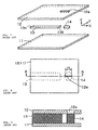
- a dielectric antenna shown in Figs. 1-3 includes a first planar conductor (a reverse conductor plate) 1 and a second planar conductor (an obverse conductor plate) 2. Disposed between the first planar conductor 1 and the second planar conductor 2 are a dielectric strip 3 and a dielectric resonator 4 spaced from each other along the X axis. Two rectangular slots 2a and 2b are provided in parallel and at equal distances from the center line of the dielectric strip 3 within the second planar conductor 2 and above the dielectric resonator 4. The center lines along the length of the slots 2a and 2b are tangent to the outer periphery of the dielectric resonator 4.
- An end portion 3a of the dielectric strip 3 is connected to a waveguide and a transmission circuit (not shown), and the other end portion 3b is an open end.
- the construction in which the dielectric strip 3 is sandwiched between the first planar conductor 1 and the second planar conductor 2 constitutes an NRD guide.
- the electromagnetic waves transmitted from the waveguide, the transmission circuit and the like to the dielectric strip 3 propagate within the dielectric strip 3 3 in an LSM (Longitudinal Section Magnetic) mode which causes an electric field having components within the YZ plane and a magnetic field having components within the XZ plane.
- LSM Longitudinal Section Magnetic
- the dielectric strip 3 and the dielectric resonator 4 are electromagnetically coupled, whereby an electromagnetic wave of an HE111 mode having electric-field components in the same direction as that of the LSM mode of the dielectric strip 3 occurs within the dielectric resonator 4.
- the electromagnetic wave is radiated by the dielectric resonator 4 via the slots 2a and 2b.
- a second dielectric resonator 4a is disposed between the dielectric strip 3 and the dielectric resonator 4. Since the other components of this embodiment are the same as those of the first embodiment, the components are given the same reference numerals, and a description thereof is omitted.
- the filtering effect is improved, making it possible to shut out harmonics or to achieve a greater bandwidth in the vicinity of the passband of the filter.
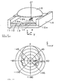
- the dielectric antenna of the first embodiment is housed in a housing 6, and a dielectric lens 5 is disposed above the slots 2a and 2b, whereby the directivity and the gain of the radiation electromagnetic wave are improved.
- the spacing between the slots was adjusted to 0.45 - 0.5 ⁇ to realize the radiation angle ⁇ (45° - 60°) thereby most of the electromagnetic waves radiated from the slots 2a and 2b are applied onto the dielectric lens 5.
- the slots 2a and 2b are disposed parallel to the center line of the dielectric resonator 4
- the slots may not be parallel to the center line of the dielectric strip 3, as illustrated by slots 2c and 2d in Fig. 6A. This is due to the reason that the coupling of the slots and the HE111 mode are achieved to a certain degree even in such an arrangement.
- Such an arrangement of slots may be used if desired for convenience in manufacturing the antennas.
- Fig. 6B shows a case in which other slots 2e and 2f which are substantially parallel to the slots 2a and 2b are disposed to the outside of the slots 2a and 2b.
- the number of slots is four, the effective opening area along the E plane becomes wider and thus the beam width can be made narrower.
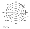
- the radiation directional pattern along the E plane of the primary radiator measured in the above specific example, is shown in Fig. 11 (the present invention) and Fig. 12 (the prior art). It can be understood from these Figs. 11 and 12 that the directivity along the E plane of the present invention having two slots is sharper than that of the prior art having one slot. That is, in Fig. 11 of the present invention, the radiation angle of a 10 dB drop of the main beam in the E plane is ⁇ 45° from the center of the main beam, while in Fig. 12 of the prior art, the radiation angle is ⁇ 110°. Further, while the antenna efficiency of the example of the present invention is 44%, the antenna efficiency of the prior art example is 30%. The antenna efficiency of the present invention is improved by approximately 10% over that of the prior art. The antenna efficiency is expressed by the ratio of the gain obtained experimentally to the directional gain calculated theoretically from the directional pattern.
Landscapes
- Aerials With Secondary Devices (AREA)
- Waveguide Aerials (AREA)
- Control Of Motors That Do Not Use Commutators (AREA)
- Waveguides (AREA)
- Radar Systems Or Details Thereof (AREA)
Claims (11)
- Eine dielektrische Antenne mit folgenden Merkmalen:einer strahlungslosen dielektrischen Führungseinrichtung, die einen dielektrischen Streifen (3) aufweist, der zwischen einem ersten planaren Leiter (1) und einem zweiten planaren Leiter (2) angeordnet ist;einem dielektrischen Resonator (4), der zwischen dem ersten planaren Leiter (1) und dem zweiten planaren Leiter (2) entlang einer Verlängerungslinie des dielektrischen Streifens (3) angeordnet ist; undeiner Mehrzahl von im wesentlichen parallelen Schlitzen (2a - 2f), die symmetrisch hinsichtlich des dielektrischen Resonators (4) in dem zweiten planaren Leiter (2) oberhalb und in der Umgebung des dielektrischen Resonators (4) angeordnet sind.
- Eine dielektrische Antenne gemäß Anspruch 1, bei der die Mehrzahl von im wesentlichen parallelen Schlitzen (2a, 2b) in einer Liniensymmetrie hinsichtlich der Mittellinie des dielektrischen Streifens (3) angeordnet ist.
- Eine dielektrische Antenne gemäß Anspruch 1, bei der die Mehrzahl von im wesentlichen parallelen Schlitzen (2a - 2f) in einer Punktsymmetrie hinsichtlich des dielektrischen Resonators (4) angeordnet ist.
- Eine dielektrische Antenne gemäß Anspruch 3, bei der die parallelen Schlitze (2a, 2b; 2e, 2f) parallel hinsichtlich der Mittellinie des dielektrischen Streifens (3) angeordnet sind.
- Eine dielektrische Antenne gemäß Anspruch 3, bei der die parallelen Schlitze (2d, 2d) mit einem spitzen Winkel hinsichtlich der Mittellinie des dielektrischen Streifens (3) angeordnet sind.
- Eine dielektrische Antenne gemäß Anspruch 1, bei der die Mehrzahl von im wesentlichen parallelen Schlitzen (2a, 2b; 2c, 2d) ein Paar von Schlitzen ist.
- Eine dielektrische Antenne gemäß Anspruch 1, bei der die Mehrzahl von im wesentlichen parallelen Schlitzen (2a, 2b, 2e, 2f) vier Schlitze sind, von denen zwei auf jeder Seite des dielektrischen Resonators (4) angeordnet sind.
- Eine dielektrische Antenne gemäß Anspruch 1, die ferner einen zweiten dielektrischen Resonator aufweist, der zwischen dem zuerst genannten dielektrischen Resonator (4) und dem dielektrischen Streifen (3) entlang der Verlängerungslinie des dielektrischen Streifens (3) angeordnet ist.
- Eine dielektrische Antenne gemäß Anspruch 1, bei der eine dielektrische Linse (5) oberhalb der Schlitze (2a - 2f) in dem zweiten planaren Leiter (2) angeordnet ist.
- Eine dielektrische Antenne gemäß Anspruch 2, bei der eine dielektrische Linse (5) oberhalb der Schlitze in dem zweiten planaren Leiter (2) angeordnet ist.
- Eine dielektrische Antenne gemäß Anspruch 3, bei der eine dielektrische Linse (5) oberhalb der Schlitze in dem zweiten planaren Leiter (2) angeordnet ist.
Applications Claiming Priority (3)
| Application Number | Priority Date | Filing Date | Title |
|---|---|---|---|
| JP7121745A JP3042364B2 (ja) | 1995-05-19 | 1995-05-19 | 誘電体アンテナ |
| JP121745/95 | 1995-05-19 | ||
| JP12174595 | 1995-05-19 |
Publications (2)
| Publication Number | Publication Date |
|---|---|
| EP0743697A1 EP0743697A1 (de) | 1996-11-20 |
| EP0743697B1 true EP0743697B1 (de) | 2003-03-12 |
Family
ID=14818840
Family Applications (1)
| Application Number | Title | Priority Date | Filing Date |
|---|---|---|---|
| EP96107604A Expired - Lifetime EP0743697B1 (de) | 1995-05-19 | 1996-05-13 | Dielektrische Antenne |
Country Status (5)
| Country | Link |
|---|---|
| US (1) | US5883601A (de) |
| EP (1) | EP0743697B1 (de) |
| JP (1) | JP3042364B2 (de) |
| CA (1) | CA2177050C (de) |
| DE (1) | DE69626565T2 (de) |
Families Citing this family (12)
| Publication number | Priority date | Publication date | Assignee | Title |
|---|---|---|---|---|
| JP3134781B2 (ja) * | 1996-07-19 | 2001-02-13 | 株式会社村田製作所 | 多層誘電体線路回路 |
| JP3119176B2 (ja) * | 1996-10-23 | 2000-12-18 | 株式会社村田製作所 | 誘電体線路用アンテナ共用分配器および送受信装置 |
| JP3186622B2 (ja) * | 1997-01-07 | 2001-07-11 | 株式会社村田製作所 | アンテナ装置および送受信装置 |
| SE508296C2 (sv) * | 1997-01-10 | 1998-09-21 | Ericsson Telefon Ab L M | Anordning vid mikrostripfördelningsnät samt gruppantenn |
| JP2000508874A (ja) * | 1997-02-06 | 2000-07-11 | ローベルト ボツシユ ゲゼルシヤフト ミツト ベシユレンクテル ハフツング | 自動車用レーダーシステムのためのマイクロ波アンテナ装置 |
| JPH10341108A (ja) * | 1997-04-10 | 1998-12-22 | Murata Mfg Co Ltd | アンテナ装置およびレーダモジュール |
| JP3120757B2 (ja) * | 1997-06-17 | 2000-12-25 | 株式会社村田製作所 | 誘電体線路装置 |
| JP2000134031A (ja) * | 1998-10-28 | 2000-05-12 | Murata Mfg Co Ltd | アンテナ装置、およびそれを用いたアンテナ、送受信装置 |
| CA2292064C (en) | 1998-12-25 | 2003-08-19 | Murata Manufacturing Co., Ltd. | Line transition device between dielectric waveguide and waveguide, and oscillator and transmitter using the same |
| US6518932B1 (en) | 1999-02-15 | 2003-02-11 | Communications Research Laboratory, Independent Administrative Institute | Radio communication device |
| JP3415817B2 (ja) * | 2000-08-28 | 2003-06-09 | アーベル・システムズ株式会社 | 太陽電池 |
| JP3473576B2 (ja) * | 2000-12-05 | 2003-12-08 | 株式会社村田製作所 | アンテナ装置および送受信装置 |
Family Cites Families (8)
| Publication number | Priority date | Publication date | Assignee | Title |
|---|---|---|---|---|
| GB1605231A (en) * | 1967-02-01 | 1985-05-09 | Emi Ltd | Aerial arrays |
| JPS60113502A (ja) * | 1983-11-24 | 1985-06-20 | Japan Radio Co Ltd | スロツトアンテナ |
| EP0295003A3 (de) * | 1987-06-09 | 1990-08-29 | THORN EMI plc | Antenne |
| KR920002439B1 (ko) * | 1988-08-31 | 1992-03-24 | 삼성전자 주식회사 | 휴대용 무선전화기의 슬로트 안테나 장치 |
| JPH04266204A (ja) * | 1991-02-20 | 1992-09-22 | Fujitsu Ltd | 微小アンテナ |
| FR2680283B1 (fr) * | 1991-08-07 | 1993-10-01 | Alcatel Espace | Antenne radioelectrique elementaire miniaturisee. |
| FR2705167B1 (fr) * | 1993-05-11 | 1995-08-04 | France Telecom | Antenne plaquee large bande a encombrement reduit, et dispositif d'emission/reception correspondant. |
| JP3128677B2 (ja) * | 1993-11-05 | 2001-01-29 | 三井造船株式会社 | 誘電体共振器付スロットアンテナ |
-
1995
- 1995-05-19 JP JP7121745A patent/JP3042364B2/ja not_active Expired - Fee Related
-
1996
- 1996-05-13 EP EP96107604A patent/EP0743697B1/de not_active Expired - Lifetime
- 1996-05-13 DE DE69626565T patent/DE69626565T2/de not_active Expired - Fee Related
- 1996-05-21 CA CA002177050A patent/CA2177050C/en not_active Expired - Fee Related
-
1997
- 1997-09-19 US US08/934,120 patent/US5883601A/en not_active Expired - Fee Related
Also Published As
| Publication number | Publication date |
|---|---|
| CA2177050A1 (en) | 1996-11-20 |
| JPH08316727A (ja) | 1996-11-29 |
| DE69626565T2 (de) | 2003-12-11 |
| DE69626565D1 (de) | 2003-04-17 |
| JP3042364B2 (ja) | 2000-05-15 |
| US5883601A (en) | 1999-03-16 |
| CA2177050C (en) | 1999-08-10 |
| EP0743697A1 (de) | 1996-11-20 |
Similar Documents
| Publication | Publication Date | Title |
|---|---|---|
| US4030048A (en) | Multimode coupling system including a funnel-shaped multimode coupler | |
| US4370659A (en) | Antenna | |
| EP0142555B1 (de) | Doppelbandige phasengesteuerte antennengruppe mit breitbandigem element und diplexer | |
| EP1158605B1 (de) | V-förmige Schlitzantenne für Zirkularpolarisation | |
| JP3725766B2 (ja) | キャビティ付きスロットアレーアンテナ | |
| US4905013A (en) | Fin-line horn antenna | |
| US5883601A (en) | Plural slot antenna fed with dielectric strip and dielectric resonators | |
| EP0577320A1 (de) | Anordnung von Hornstrahlern mit stufenförmigem Septumpolarisator | |
| CA1211208A (en) | Electromagnetic wave radiator and use thereof in an electronic sweep antenna | |
| EP1396903B1 (de) | Dielektrischer Wellenleiter und dessen Abzweigstruktur | |
| EP0468413A2 (de) | Ebene Antenne mit hohem Gewinn und grossem Wirkungsgrad | |
| US3977006A (en) | Compensated traveling wave slotted waveguide feed for cophasal arrays | |
| US6094175A (en) | Omni directional antenna | |
| CA2095052C (en) | Dual-mode communication antenna | |
| CA1135548A (en) | Wide scan quasi-optical frequency diplexer | |
| US11450973B1 (en) | All metal wideband tapered slot phased array antenna | |
| US3380057A (en) | Dual band ridged feed horn | |
| US3857112A (en) | Broadband quarter-wave plate assembly | |
| EP0666609B1 (de) | Komparator | |
| JPH0666577B2 (ja) | マイクロストリツプアンテナ | |
| JPH0722803A (ja) | 偏分波器 | |
| US6130649A (en) | Polarizer for exciting an antenna | |
| JPH06334431A (ja) | マイクロストリップアンテナ | |
| US7009571B2 (en) | Method and apparatus for forming symmetrical energy patterns in beam forming antennas | |
| US6677910B2 (en) | Compact primary radiator |
Legal Events
| Date | Code | Title | Description |
|---|---|---|---|
| PUAI | Public reference made under article 153(3) epc to a published international application that has entered the european phase |
Free format text: ORIGINAL CODE: 0009012 |
|
| 17P | Request for examination filed |
Effective date: 19960513 |
|
| AK | Designated contracting states |
Kind code of ref document: A1 Designated state(s): DE FR GB |
|
| 17Q | First examination report despatched |
Effective date: 20001204 |
|
| GRAH | Despatch of communication of intention to grant a patent |
Free format text: ORIGINAL CODE: EPIDOS IGRA |
|
| GRAH | Despatch of communication of intention to grant a patent |
Free format text: ORIGINAL CODE: EPIDOS IGRA |
|
| GRAA | (expected) grant |
Free format text: ORIGINAL CODE: 0009210 |
|
| AK | Designated contracting states |
Designated state(s): DE FR GB |
|
| REG | Reference to a national code |
Ref country code: GB Ref legal event code: FG4D |
|
| REF | Corresponds to: |
Ref document number: 69626565 Country of ref document: DE Date of ref document: 20030417 Kind code of ref document: P |
|
| ET | Fr: translation filed | ||
| PLBE | No opposition filed within time limit |
Free format text: ORIGINAL CODE: 0009261 |
|
| STAA | Information on the status of an ep patent application or granted ep patent |
Free format text: STATUS: NO OPPOSITION FILED WITHIN TIME LIMIT |
|
| 26N | No opposition filed |
Effective date: 20031215 |
|
| PGFP | Annual fee paid to national office [announced via postgrant information from national office to epo] |
Ref country code: DE Payment date: 20080522 Year of fee payment: 13 |
|
| PGFP | Annual fee paid to national office [announced via postgrant information from national office to epo] |
Ref country code: GB Payment date: 20080514 Year of fee payment: 13 |
|
| GBPC | Gb: european patent ceased through non-payment of renewal fee |
Effective date: 20090513 |
|
| REG | Reference to a national code |
Ref country code: FR Ref legal event code: ST Effective date: 20100129 |
|
| PG25 | Lapsed in a contracting state [announced via postgrant information from national office to epo] |
Ref country code: FR Free format text: LAPSE BECAUSE OF NON-PAYMENT OF DUE FEES Effective date: 20090602 |
|
| PGFP | Annual fee paid to national office [announced via postgrant information from national office to epo] |
Ref country code: FR Payment date: 20080514 Year of fee payment: 13 |
|
| PG25 | Lapsed in a contracting state [announced via postgrant information from national office to epo] |
Ref country code: GB Free format text: LAPSE BECAUSE OF NON-PAYMENT OF DUE FEES Effective date: 20090513 |
|
| PG25 | Lapsed in a contracting state [announced via postgrant information from national office to epo] |
Ref country code: DE Free format text: LAPSE BECAUSE OF NON-PAYMENT OF DUE FEES Effective date: 20091201 |