EP0743685A2 - Nonvolatile semiconductor memory utilizing polarization of ferroelectric material - Google Patents
Nonvolatile semiconductor memory utilizing polarization of ferroelectric material Download PDFInfo
- Publication number
- EP0743685A2 EP0743685A2 EP96108018A EP96108018A EP0743685A2 EP 0743685 A2 EP0743685 A2 EP 0743685A2 EP 96108018 A EP96108018 A EP 96108018A EP 96108018 A EP96108018 A EP 96108018A EP 0743685 A2 EP0743685 A2 EP 0743685A2
- Authority
- EP
- European Patent Office
- Prior art keywords
- film
- semiconductor memory
- nonvolatile semiconductor
- gate electrode
- ferroelectric material
- Prior art date
- Legal status (The legal status is an assumption and is not a legal conclusion. Google has not performed a legal analysis and makes no representation as to the accuracy of the status listed.)
- Granted
Links
- 239000004065 semiconductor Substances 0.000 title claims abstract description 47
- 239000000463 material Substances 0.000 title claims description 43
- 230000010287 polarization Effects 0.000 title description 24
- 239000000758 substrate Substances 0.000 claims abstract description 45
- 239000012212 insulator Substances 0.000 claims abstract description 21
- VYPSYNLAJGMNEJ-UHFFFAOYSA-N Silicium dioxide Chemical compound O=[Si]=O VYPSYNLAJGMNEJ-UHFFFAOYSA-N 0.000 claims abstract description 19
- 229910052814 silicon oxide Inorganic materials 0.000 claims abstract description 19
- XUIMIQQOPSSXEZ-UHFFFAOYSA-N Silicon Chemical compound [Si] XUIMIQQOPSSXEZ-UHFFFAOYSA-N 0.000 claims abstract description 15
- 229910052710 silicon Inorganic materials 0.000 claims abstract description 15
- 239000010703 silicon Substances 0.000 claims abstract description 15
- 229910052581 Si3N4 Inorganic materials 0.000 claims abstract description 11
- HQVNEWCFYHHQES-UHFFFAOYSA-N silicon nitride Chemical compound N12[Si]34N5[Si]62N3[Si]51N64 HQVNEWCFYHHQES-UHFFFAOYSA-N 0.000 claims abstract description 11
- 229910012463 LiTaO3 Inorganic materials 0.000 claims description 10
- 229910009567 YMnO3 Inorganic materials 0.000 claims description 9
- XKENYNILAAWPFQ-UHFFFAOYSA-N dioxido(oxo)germane;lead(2+) Chemical compound [Pb+2].[O-][Ge]([O-])=O XKENYNILAAWPFQ-UHFFFAOYSA-N 0.000 abstract description 16
- 239000010408 film Substances 0.000 description 194
- 238000000034 method Methods 0.000 description 21
- 230000005684 electric field Effects 0.000 description 19
- 229920002120 photoresistant polymer Polymers 0.000 description 18
- 238000004519 manufacturing process Methods 0.000 description 13
- QVGXLLKOCUKJST-UHFFFAOYSA-N atomic oxygen Chemical compound [O] QVGXLLKOCUKJST-UHFFFAOYSA-N 0.000 description 10
- 239000001301 oxygen Substances 0.000 description 10
- 229910052760 oxygen Inorganic materials 0.000 description 10
- 238000002955 isolation Methods 0.000 description 9
- 239000010410 layer Substances 0.000 description 9
- 238000004544 sputter deposition Methods 0.000 description 9
- ATJFFYVFTNAWJD-UHFFFAOYSA-N Tin Chemical compound [Sn] ATJFFYVFTNAWJD-UHFFFAOYSA-N 0.000 description 8
- 230000003647 oxidation Effects 0.000 description 7
- 238000007254 oxidation reaction Methods 0.000 description 7
- 230000002093 peripheral effect Effects 0.000 description 7
- 239000004020 conductor Substances 0.000 description 6
- 239000011229 interlayer Substances 0.000 description 6
- 229910052451 lead zirconate titanate Inorganic materials 0.000 description 6
- 238000002441 X-ray diffraction Methods 0.000 description 5
- 230000015572 biosynthetic process Effects 0.000 description 5
- 239000000203 mixture Substances 0.000 description 5
- 230000001590 oxidative effect Effects 0.000 description 5
- 230000007547 defect Effects 0.000 description 4
- 229910052732 germanium Inorganic materials 0.000 description 4
- 229910052785 arsenic Inorganic materials 0.000 description 3
- RQNWIZPPADIBDY-UHFFFAOYSA-N arsenic atom Chemical compound [As] RQNWIZPPADIBDY-UHFFFAOYSA-N 0.000 description 3
- 239000013078 crystal Substances 0.000 description 3
- 230000006866 deterioration Effects 0.000 description 3
- 238000011161 development Methods 0.000 description 3
- 238000001312 dry etching Methods 0.000 description 3
- 229910052745 lead Inorganic materials 0.000 description 3
- 238000003980 solgel method Methods 0.000 description 3
- QTBSBXVTEAMEQO-UHFFFAOYSA-N Acetic acid Chemical compound CC(O)=O QTBSBXVTEAMEQO-UHFFFAOYSA-N 0.000 description 2
- 229910000838 Al alloy Inorganic materials 0.000 description 2
- IJGRMHOSHXDMSA-UHFFFAOYSA-N Atomic nitrogen Chemical compound N#N IJGRMHOSHXDMSA-UHFFFAOYSA-N 0.000 description 2
- MYMOFIZGZYHOMD-UHFFFAOYSA-N Dioxygen Chemical compound O=O MYMOFIZGZYHOMD-UHFFFAOYSA-N 0.000 description 2
- 239000003990 capacitor Substances 0.000 description 2
- 238000010276 construction Methods 0.000 description 2
- 229910001873 dinitrogen Inorganic materials 0.000 description 2
- 229910001882 dioxygen Inorganic materials 0.000 description 2
- 238000004518 low pressure chemical vapour deposition Methods 0.000 description 2
- 239000000843 powder Substances 0.000 description 2
- LIVNPJMFVYWSIS-UHFFFAOYSA-N silicon monoxide Chemical compound [Si-]#[O+] LIVNPJMFVYWSIS-UHFFFAOYSA-N 0.000 description 2
- ZAMOUSCENKQFHK-UHFFFAOYSA-N Chlorine atom Chemical compound [Cl] ZAMOUSCENKQFHK-UHFFFAOYSA-N 0.000 description 1
- 229910052782 aluminium Inorganic materials 0.000 description 1
- XAGFODPZIPBFFR-UHFFFAOYSA-N aluminium Chemical compound [Al] XAGFODPZIPBFFR-UHFFFAOYSA-N 0.000 description 1
- 238000000137 annealing Methods 0.000 description 1
- 230000004888 barrier function Effects 0.000 description 1
- 238000006243 chemical reaction Methods 0.000 description 1
- 239000000460 chlorine Substances 0.000 description 1
- 229910052801 chlorine Inorganic materials 0.000 description 1
- 238000004891 communication Methods 0.000 description 1
- 238000011109 contamination Methods 0.000 description 1
- 238000000151 deposition Methods 0.000 description 1
- 230000008021 deposition Effects 0.000 description 1
- 238000009792 diffusion process Methods 0.000 description 1
- HHFAWKCIHAUFRX-UHFFFAOYSA-N ethoxide Chemical compound CC[O-] HHFAWKCIHAUFRX-UHFFFAOYSA-N 0.000 description 1
- 239000007789 gas Substances 0.000 description 1
- GNPVGFCGXDBREM-UHFFFAOYSA-N germanium atom Chemical compound [Ge] GNPVGFCGXDBREM-UHFFFAOYSA-N 0.000 description 1
- YBMRDBCBODYGJE-UHFFFAOYSA-N germanium oxide Inorganic materials O=[Ge]=O YBMRDBCBODYGJE-UHFFFAOYSA-N 0.000 description 1
- 238000010438 heat treatment Methods 0.000 description 1
- 229910000464 lead oxide Inorganic materials 0.000 description 1
- HFGPZNIAWCZYJU-UHFFFAOYSA-N lead zirconate titanate Chemical compound [O-2].[O-2].[O-2].[O-2].[O-2].[Ti+4].[Zr+4].[Pb+2] HFGPZNIAWCZYJU-UHFFFAOYSA-N 0.000 description 1
- 230000007774 longterm Effects 0.000 description 1
- 229910052748 manganese Inorganic materials 0.000 description 1
- 238000005259 measurement Methods 0.000 description 1
- 229910052751 metal Inorganic materials 0.000 description 1
- 239000002184 metal Substances 0.000 description 1
- 238000012986 modification Methods 0.000 description 1
- 230000004048 modification Effects 0.000 description 1
- PVADDRMAFCOOPC-UHFFFAOYSA-N oxogermanium Chemical compound [Ge]=O PVADDRMAFCOOPC-UHFFFAOYSA-N 0.000 description 1
- YEXPOXQUZXUXJW-UHFFFAOYSA-N oxolead Chemical compound [Pb]=O YEXPOXQUZXUXJW-UHFFFAOYSA-N 0.000 description 1
- 238000000059 patterning Methods 0.000 description 1
- 241000894007 species Species 0.000 description 1
- 238000003860 storage Methods 0.000 description 1
- 229910052715 tantalum Inorganic materials 0.000 description 1
- 239000010409 thin film Substances 0.000 description 1
Images


Classifications
-
- H—ELECTRICITY
- H01—ELECTRIC ELEMENTS
- H01L—SEMICONDUCTOR DEVICES NOT COVERED BY CLASS H10
- H01L29/00—Semiconductor devices adapted for rectifying, amplifying, oscillating or switching, or capacitors or resistors with at least one potential-jump barrier or surface barrier, e.g. PN junction depletion layer or carrier concentration layer; Details of semiconductor bodies or of electrodes thereof ; Multistep manufacturing processes therefor
- H01L29/66—Types of semiconductor device ; Multistep manufacturing processes therefor
- H01L29/68—Types of semiconductor device ; Multistep manufacturing processes therefor controllable by only the electric current supplied, or only the electric potential applied, to an electrode which does not carry the current to be rectified, amplified or switched
- H01L29/76—Unipolar devices, e.g. field effect transistors
- H01L29/772—Field effect transistors
- H01L29/78—Field effect transistors with field effect produced by an insulated gate
- H01L29/78391—Field effect transistors with field effect produced by an insulated gate the gate comprising a layer which is used for its ferroelectric properties
Definitions
- the present invention relates to a nonvolatile semiconductor memory, and more specifically to a nonvolatile semiconductor memory configured to store information by utilizing polarization of a ferroelectric material.
- a nonvolatile semiconductor memory utilizing a ferroelectric material as a medium for storing information has an advantage that if deterioration of a ferroelectric material film does not occur, information can be stored for a long term of time, and further, is expected that it can make it possible to reduce a memory cell size and therefore to realize a memory having a large storage capacity.
- a device isolation oxide film (field oxide) 102 is formed by a selective oxidation such as a LOCOS (local oxidation of silicon) process, and within an active region confined by the device isolation oxide film, a gate electrode 103 is formed through a gate insulator film on the surface of the substrate.
- a source region 104 and a drain region 105 are formed in a surface region of the substrate at opposite sides of the gate electrode 103, so as to locate the gate electrode between the source region and the drain region.
- a first interlayer insulator film 106 is formed to cover a whole surface of the substrate, and a Pt film 107 is formed on the first interlayer insulator film 106, above a position of the gate electrode 103. Furthermore, a PZT (PbZr 1-x Ti x O 3 ) film 108 is formed to cover the Pt film 107. A second interlayer insulator film 109 is formed to cover a whole surface of the substrate including the PZT film 108. In addition, contact holes are formed to reach the drain region 105 and the PZT film 108, respectively, and an aluminum wiring conductor 110 is formed on the second interlayer insulator film 109 to contact with the drain region 105 and the PZT film 108 through the contact holes.
- PZT PbZr 1-x Ti x O 3
- FIG. 2 there is shown a diagrammatic section view illustrating another example of a conventional nonvolatile semiconductor memory utilizing a ferroelectric material film, in which a gate insulator film of a transistor is formed of a ferroelectric material film.
- a device isolation oxide film 2 is formed on a principal surface of a P-type silicon substrate 1, and a ferroelectric material film 4C is formed on the principal surface of the substrate 1 to constitute a gate insulator film.
- a gate electrode 5A is formed on the ferroelectric material film 4C, and a source region 7 and a drain region 8 are formed in a surface region of the substrate at opposite sides of the gate electrode 5A, so as to locate the gate electrode between the source region and the drain region.
- the ferroelectric material of the gate insulator film which is now under consideration, is BaMgF 4 and PbZr 1-x Ti x O 3 .
- each memory cell consists of a transistor part and a memory part, the structure is complicated. This is inconvenient to microminiaturization.
- a coercive electric field (applied electric field when polarization reversal starts) of the PbZr 1-x Ti x O 3 film is on the order of 80 kV/cm, and a dielectric constant of the PbZr 1-x Ti x O 3 film is on the order of 1000.
- the natural oxide film is not an intentionally formed film, the natural oxide film is not so good in film quality, so that there is high possibility that if a high electric field as mentioned above is applied, the natural oxide film is broken down.
- the PbZr 1-x Ti x O 3 film is formed to have a thickness of 100 nm, it is necessary to apply a voltage of 0.8 V across the PbZr 1-x Ti x O 3 film in order to apply a necessary coercive electric field.
- the gate insulator film is formed of BaMgF 4 , no natural oxide film is formed since BaMgF 4 does not include an oxidizing specie.
- polarizability of this material is relatively low.
- the BaMgF 4 film contains a crystal defect, the polarizability further lowers. Therefore, in order to constitute a satisfactory memory, it is necessary to form a BaMgF 4 film having an excellent film quality, namely, less crystal defect. However, this is not so easy because of difference in lattice constant between BaMgF 4 and a silicon substrate and because of other causes.
- ferroelectric materials other than oxides having a low dielectric constant Since there exist ferroelectric materials other than oxides having a low dielectric constant, it is possible to prevent formation of the natural oxide by using the ferroelectric materials other than oxides. However, these ferroelectric materials are small in polarizability and poor in heat resistive property, and therefore, it is difficult to use these ferroelectric materials as a material used for manufacturing a semiconductor device.
- Another object of the present invention is to provide a nonvolatile semiconductor memory configured to store information by utilizing polarization of a ferroelectric material, the nonvolatile semiconductor memory having a simple construction and a high reliability and being easy to manufacture and to microminiaturize, the nonvolatile semiconductor memory being able to be driven with a low voltage.
- a nonvolatile semiconductor memory comprising a semiconductor substrate, a gate electrode formed through a gate insulator film on a principal surface of the semiconductor substrate, a pair of source/drain regions formed in a principal surface region of the semiconductor substrate to locate the gate electrode between the pair of source/drain regions, the gate insulator film being formed of a first insulating film in contact with the principal surface of the semiconductor substrate, and a second insulating film formed on the first insulating film, the second insulating film being formed of a ferroelectric oxide having a dielectric constant of not larger than 50.
- the second insulating film includes a material selected from a group consisting of Pb 5 Ge 3 O 11 , LiTaO 3 , YMnO 3 , YbMnO 3 , ErMnO 3 and HoMnO 3 .
- the first insulating film is formed of a film selected from the group consisting of a silicon oxide film, a silicon oxynitride film and a laminated layer composed of an underlying silicon oxide film and an overlying silicon nitride film.
- a silicon oxide film or a silicon nitride film is preferably formed between the second insulating film and the gate electrode.
- the ferroelectric material film provided as the gate insulator film is required to have a film thickness on the order of 50 nm to 200 nm. Assuming that the ferroelectric material film has the coercive electric field of 80 kV/cm, it is necessary to apply a voltage of 0.4 V to 1.6 V across the ferroelectric material film. Under this condition, on the other hand, a voltage of 0.2 V is applied across the natural oxide film. Accordingly, it is possible to start polarization by applying a voltage of 0.6 V to 1.8 V to the gate electrode. Thus, even considering that it is necessary to apply a voltage higher than that voltage by several ten percents in order to cause a complete polarization, it is possible to drive the memory with an extremely low voltage.
- oxide ferroelectric materials are not deteriorated even if a semiconductor device manufacturing temperature is applied.
- FIG. 3A to 3D there are shown diagrammatic sectional views illustrating a process for manufacturing a first embodiment of the nonvolatile semiconductor memory in accordance with the present invention utilizing polarization of a ferroelectric material.
- a device isolation oxide film (field oxide) 2 is formed by a selective oxidation such as a LOCOS (local oxidation of silicon) process.
- a thermal oxidation is carried out in a low pressure atmosphere (for example, 1 Torr) at a temperature of 800°C, so as to form a thin oxide film having a thickness of 1.5 nm on the principal surface of the substrate 1.
- the thermal oxide film is lamp-heated within a NH 3 atmosphere so that an oxynitride film 3 is formed on the surface of the substrate.
- an ethylate (or ethoxide) of lead and an ethylate of germanium are prepared, and then, mixed to have a composition ratio of 5 : 3.
- the obtained mixture is deposited on the oxynitride film 3 by a sol gel process.
- an annealing is carried out within a dry oxygen atmosphere at 650°C for one hour. With this treatment, a film 4 of Pb 5 Ge 3 O 11 (lead germanate film) having a thickness of 100 nm is formed on the oxynitride film 3 as shown in Figure 3A.
- a dry etching using a chlorine containing gas is performed to pattern the TiN film 5 so as to form a gate electrode.
- a chlorine containing gas is performed to pattern the TiN film 5 so as to form a gate electrode.
- arsenic (As) is ion-implanted to form a source region 7 and a drain region 8 in a surface region of the substrate 1, as shown in Figure 3C.
- the photoresist film 6 is ashed in an oxygen plasma so that the photoresist film 6 is removed as shown in Figure 3D.
- the gate electrode (TiN film 5) is formed on the Pb 5 Ge 3 O 11 film 4 at the room temperature.
- a heat treatment is performed after formation of an upper electrode, and in the case that the gate electrode itself is formed at a high temperature process, it is preferred to form a silicon oxide film or a silicon nitride film, at a boundary between the Pb 5 Ge 3 O 11 film 4 and the gate electrode, namely, on the Pb 5 Ge 3 O 11 film 4 before deposition of the gate electrode layer, in order to prevent reaction between the Pb 5 Ge 3 O 11 film 4 and the gate electrode metal.
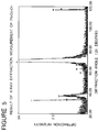
- a lead germanate film was formed on a whole surface of a silicon substrate by a sol gel process. Scanning electron microscope photographs of a surface and a section of the lead germanate film thus formed are shown in Figures 4A and 4B. From these photographs, it would be seen that a film having a smooth surface and a thickness on the order of 900 ⁇ is formed on the silicon substrate. Furthermore, the result of an X-ray diffraction measurement of the lead germanate film thus formed is shown in Figure 5. It would also be seen that the lead germanate film thus formed is polycrystalline.
- a TiN film (used for constituting the gate electrode) was formed on the lead germanate film thus formed, and a dielectric constant and a hysteresis characteristics were measured.
- the result of the measurement is that the dielectric constant is about 18.3 and the residual dielectric polarization is about 1.2 ⁇ C/cm 2 .
- a lead germanate film having a thickness of 3000 ⁇ was formed on a Pt electrode by the above mentioned sol gel process.
- This lead germanate film having the thickness of 3000 ⁇ had the coercive electric field of 14 kV/cm and the residual dielectric polarization of about 1.6 ⁇ C/cm 2 . Therefore, it would be understood that polarization reversal occurs by applying a voltage on the order of 0.4 V to the lead germanate film.
- the oxynitride film having the thickness of 2 nm converted into an oxide film thickness under the ferroelectric material film, there is formed the oxynitride film having the thickness of 2 nm converted into an oxide film thickness. Therefore, in the case of polarizing the lead germanate film having the thickness of 100 nm used in the actual device, a voltage applied across the natural oxide film is on the order of 0.013 V. This means that the natural oxide film is applied with only a voltage of 1/300 of the voltage applied in the case of the PZT film. This is considered to be attributable to the fact that both the dielectric constant and the coercive electric field of the ferroelectric material became small.
- an electric charge required to actually operate the device as a memory is on the order of 0.5 ⁇ C/cm 2 . Therefore, the residual dielectric polarization of about 1.6 ⁇ C/cm 2 , which could have been confirmed at present, is a satisfactory value.
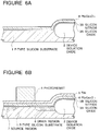
- FIG. 6A to 6D there are shown diagrammatic sectional views illustrating a process for manufacturing a second embodiment of the nonvolatile semiconductor memory in accordance with the present invention utilizing polarization of a ferroelectric material.
- a device isolation oxide film 2 is formed by a selective oxidation process. Then, the substrate 1 is heated to a temperature of 800°C, and then, is exposed to an oxygen gas diluted by a nitrogen gas, so that a silicon oxide film 3A having a thickness of 1.5 nm is formed on the surface of the substrate 1. Furthermore, a silicon nitride film 3B having a thickness of about 2 nm is formed on the silicon oxide film 3A by a low pressure CVD process.
- an oxide of Pb and Ge is deposited to form a film having a thickness of about 200 nm.
- the molar ratio of Pb and Ge in the target is 2.5 : 1. Namely, Pb is richer than Ge.
- the sputtering condition is that the substrate temperature is 450°C, and the plasma is generated in an atmosphere consisting of 90% of Ar and 10% of oxygen under a pressure of 6 mTorr.
- the reason for why the proportion of Pb drops as compared with the molar ratio in the target, is considered to be that lead evaporated at the temperature of 450°C.
- a TiN film 5 having a thickness of 100 nm is deposited on the Pb 5 Ge 3 O 11 film 4 by a sputtering.
- a photoresist film is deposited, and exposure and development are carried out to form a patterned photoresist film 6 having a pattern for the gate electrode.
- arsenic (As) is ion-implanted to form a source region 7 and a drain region 8 in a surface region of the substrate 1, as shown in Figure 6B.
- a dry etching is performed to remove the TiN film 5 and the Pb 5 Ge 3 O 11 film 4 which are not covered with the patterned photoresist film 6, so that a gate electrode is formed as shown in Figure 6C.
- a silicon oxide film having a thickness of 200 nm is deposited by a CVD process with a substrate temperature of 400°C, so as to form an interlayer insulator film 9 which completely covers the whole surface.
- a contact hole is formed to reach the drain region 8, and an aluminum alloy film is deposited and patterned to form a wiring conductor 10 contacting to the drain region 8 through the contact hole, as shown in Figure 6D.
- This wiring conductor 10 constitutes a bit line.
- the source region 7 is connected in common to a source region of other memory cells by means of a diffused layer (not shown) formed in the substrate.
- peripheral circuit can be formed in the same process as that for manufacturing a peripheral circuit in a conventional memory. In the present invention, however, it is preferred to previously form the peripheral circuit, prior to formation of the memory cells. But, if the peripheral circuit can be formed in a process of not higher than 700°C, the peripheral circuit can be formed after the formation of the memory cells.
- the source region is connected in common to the source region of other memory cells by means of the diffused layer formed in the substrate, but can be connected through a wiring conductor.
- the transistor is on-off controlled by direction of the polarization of the Pb 5 Ge 3 O 11 film 4. Therefore, the memory as mentioned above can be operated as a nonvolatile memory.
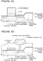
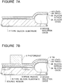
- FIGS. 7A to 7D there are shown diagrammatic sectional views illustrating a process for manufacturing a third embodiment of the nonvolatile semiconductor memory in accordance with the present invention utilizing polarization of a ferroelectric material.
- a device isolation oxide film 2 is formed by a selective oxidation process. Then, the substrate 1 is heated to a temperature of 800°C, and then, is exposed to an oxygen gas diluted by a nitrogen gas, so that a silicon oxide film 3A having a thickness of 1.5 nm is formed on the surface of the substrate 1. Furthermore, a silicon nitride film 3B having a thickness of about 3 nm is formed on the silicon oxide film 3A by a low pressure CVD process.
- an oxide of Li and Ta is deposited to form a film having a thickness of about 200 nm.
- the sputtering condition is that the substrate temperature is 560°C, and the plasma is generated in an atmosphere consisting of 90% of Ar and 10% of oxygen under a pressure of 6 mTorr.
- a molar ratio of Li : Ta is about 1 : 1.
- an oxidizing treatment is performed on this film within an oxygen atmosphere at a temperature of 1100°C for thirty seconds. From the X-ray diffraction analysis of this film, it was confirmed that the film thus formed is a LiTaO 3 film 4A ( Figure 7A).
- a TiN film 5 having a thickness of 100 nm is deposited on the LiTaO 3 film 4A thus formed, by sputtering at a room temperature.
- a photoresist film is deposited, and exposure and development are carried out to form a patterned photoresist film 6 having a pattern for the gate electrode.
- arsenic (As) is ion-implanted to form a source region 7 and a drain region 8 in a surface region of the substrate 1, as shown in Figure 7B.
- a dry etching is performed to remove the TiN film 5 and the LiTaO 3 film 4A which are not covered with the patterned photoresist film 6, so that a gate electrode is formed as shown in Figure 7C.
- a silicon oxide film having a thickness of 200 nm is deposited by a CVD process with a substrate temperature of 400°C, so as to form an interlayer insulator film 9 which completely covers the whole surface.
- a contact hole is formed to reach the drain region 8, and an aluminum alloy film is deposited and patterned to form a wiring conductor 10 contacting to the drain region 8 through the contact hole, as shown in Figure 7D.
- This wiring conductor 10 constitutes a bit line.
- the source region 7 is connected in common to source regions of other memory cells by means of a diffused layer (not shown) formed in the substrate, similarly to the other embodiments.
- the method for manufacturing the third embodiment of the memory cell in the nonvolatile semiconductor memory has been described.
- the reason for this is that since Li is easy to diffuse, contamination of the device must be made as small as possible.
- the silicon nitride film formed under the LiTaO 3 film is a film required as a barrier for preventing diffusion of Li.
- the silicon oxide film is provided as a lowermost layer, for the purpose of reducing energy levels at a boundary so as to elevate performance of the transistor.
- the dielectric constant of the LiTaO 3 film 4A thus formed was about 45. It was confirmed that the transistor can be on-off controlled by direction of the polarization of the LiTaO 3 film 4A, and therefore, this memory as mentioned above can be operated as a nonvolatile memory.
- the fourth embodiment is characterized in that a YMnO 3 film 4B is formed in place of the LiTaO 3 film 4A in the third embodiment. Since the process other than a step of forming the YMnO 3 film 4B is the same as a corresponding process of the third embodiment, only the step of forming the YMnO 3 film 4B will be described in the following.
- an oxide of Y and Mn is deposited on the silicon nitride film 3B to form a film having a thickness of about 150 nm.
- the sputtering condition is that the substrate temperature is 600°C, and the plasma is generated in an atmosphere consisting of 90% of Ar and 10% of oxygen under a pressure of 10 mTorr.
- a molar ratio of Y : Mn is about 1 : 1.
- an oxidizing treatment is performed on this film within an oxygen atmosphere at a temperature of 800°C for sixty seconds. From the X-ray diffraction analysis of this film, it was confirmed that the film thus formed is a YMnO 3 film ( Figure 7A).
- the nonvolatile semiconductor memory in accordance with the present invention is characterized in that a gate insulator film of a MOS transistor is formed of a ferroelectric material having a dielectric constant of not larger than 50.
- a gate insulator film of a MOS transistor is formed of a ferroelectric material having a dielectric constant of not larger than 50.
Landscapes
- Engineering & Computer Science (AREA)
- Microelectronics & Electronic Packaging (AREA)
- Power Engineering (AREA)
- Physics & Mathematics (AREA)
- Ceramic Engineering (AREA)
- Condensed Matter Physics & Semiconductors (AREA)
- General Physics & Mathematics (AREA)
- Computer Hardware Design (AREA)
- Semiconductor Memories (AREA)
- Non-Volatile Memory (AREA)
Abstract
Description
- The present invention relates to a nonvolatile semiconductor memory, and more specifically to a nonvolatile semiconductor memory configured to store information by utilizing polarization of a ferroelectric material.
- A nonvolatile semiconductor memory utilizing a ferroelectric material as a medium for storing information, has an advantage that if deterioration of a ferroelectric material film does not occur, information can be stored for a long term of time, and further, is expected that it can make it possible to reduce a memory cell size and therefore to realize a memory having a large storage capacity.
- Reza Moazzami et al, "A Ferroelectric DRAM Cell for High-Density NVRAM's", IEEE ELECTRON DEVICE LETTERS, Vol.11, No.10, October 1990, Pages 454-456, (the disclosure of which is incorporated by reference in its entirety into this application) proposed one example of the above mentioned conventional nonvolatile semiconductor memory, in which a capacitor dielectric of a DRAM memory cell capacitor is formed of lead zirconate titanate (PbZr1-xTixO3)
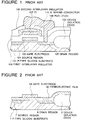
- Referring to Figure 1, there is shown a diagrammatic sectional view of the nonvolatile semiconductor memory proposed by Reza Moazzami et al. On a principal surface of a P-type silicon substrate 101, a device isolation oxide film (field oxide) 102 is formed by a selective oxidation such as a LOCOS (local oxidation of silicon) process, and within an active region confined by the device isolation oxide film, a
gate electrode 103 is formed through a gate insulator film on the surface of the substrate. A source region 104 and adrain region 105 are formed in a surface region of the substrate at opposite sides of thegate electrode 103, so as to locate the gate electrode between the source region and the drain region. A first interlayer insulator film 106 is formed to cover a whole surface of the substrate, and aPt film 107 is formed on the first interlayer insulator film 106, above a position of thegate electrode 103. Furthermore, a PZT (PbZr1-xTixO3) film 108 is formed to cover thePt film 107. A secondinterlayer insulator film 109 is formed to cover a whole surface of the substrate including the PZT film 108. In addition, contact holes are formed to reach thedrain region 105 and the PZT film 108, respectively, and analuminum wiring conductor 110 is formed on the secondinterlayer insulator film 109 to contact with thedrain region 105 and the PZT film 108 through the contact holes. - Referring to Figure 2, there is shown a diagrammatic section view illustrating another example of a conventional nonvolatile semiconductor memory utilizing a ferroelectric material film, in which a gate insulator film of a transistor is formed of a ferroelectric material film.
- As shown in Figure 2, a device
isolation oxide film 2 is formed on a principal surface of a P-type silicon substrate 1, and aferroelectric material film 4C is formed on the principal surface of thesubstrate 1 to constitute a gate insulator film. Agate electrode 5A is formed on theferroelectric material film 4C, and asource region 7 and adrain region 8 are formed in a surface region of the substrate at opposite sides of thegate electrode 5A, so as to locate the gate electrode between the source region and the drain region. - This structure is very effective in reducing the cell size, since the transistor itself has a memory part. The ferroelectric material of the gate insulator film, which is now under consideration, is BaMgF4 and PbZr1-xTixO3.
- A construction and an operation principle of this type memory cell is discussed in, for example, "Nonvolatile Memory FET Utilizing A Ferroelectric Material Thin Film", Report of (Japanese) Society of Electronic Communication, CPM-78-46 : 1, 1978, the disclosure of which is incorporated by reference in its entirety into this application.
- In the conventional memory cell shown in Figure 1, since the electrode underlying the ferroelectric material film has to be formed of a material such as Pt, which is hard to etch or pattern, a fine patterning is difficult. In addition, since each memory cell consists of a transistor part and a memory part, the structure is complicated. This is inconvenient to microminiaturization.
- On the other hand, in the second conventional example shown in Figure 2, since a material, such as PbZr1-xTixO3, having a high dielectric constant, is used as the ferroelectric material, it is difficult to form a highly reliable device. In addition, it is difficult to realize a low voltage driving, which is recently strongly demanded by users. The reason for these disadvantages will be described in the following.
- In the case that a PbZr1-xTixO3 film is used as the gate insulating film, when the PbZr1-xTixO3 film is deposited directly on a silicon substrate, a natural oxide (or native oxide) layer having a thickness of about 2 nm is inevitably formed at a boundary of the silicon substrate.
- A coercive electric field (applied electric field when polarization reversal starts) of the PbZr1-xTixO3 film is on the order of 80 kV/cm, and a dielectric constant of the PbZr1-xTixO3 film is on the order of 1000. On the other hand, a dielectric constant of a silicon oxide film is on the order of 4. Therefore, when the coercive electric field is applied across the PbZr1-xTixO3 film, an electric field as high as

- Here, assuming that the PbZr1-xTixO3 film is formed to have a thickness of 100 nm, it is necessary to apply a voltage of 0.8 V across the PbZr1-xTixO3 film in order to apply a necessary coercive electric field. Incidentally, in order to cause a complete polarization reversal, it is necessary to apply a voltage which is higher than 0.8 V by several ten percents. At this time, on the other hand, a voltage of

- On the other hand, if the gate insulator film is formed of BaMgF4, no natural oxide film is formed since BaMgF4 does not include an oxidizing specie. However, polarizability of this material is relatively low. In addition, if the BaMgF4 film contains a crystal defect, the polarizability further lowers. Therefore, in order to constitute a satisfactory memory, it is necessary to form a BaMgF4 film having an excellent film quality, namely, less crystal defect. However, this is not so easy because of difference in lattice constant between BaMgF4 and a silicon substrate and because of other causes.
- Since there exist ferroelectric materials other than oxides having a low dielectric constant, it is possible to prevent formation of the natural oxide by using the ferroelectric materials other than oxides. However, these ferroelectric materials are small in polarizability and poor in heat resistive property, and therefore, it is difficult to use these ferroelectric materials as a material used for manufacturing a semiconductor device.
- Accordingly, it is an object of the present invention to provide a nonvolatile semiconductor memory which has overcome the above mentioned defects of the conventional ones.
- Another object of the present invention is to provide a nonvolatile semiconductor memory configured to store information by utilizing polarization of a ferroelectric material, the nonvolatile semiconductor memory having a simple construction and a high reliability and being easy to manufacture and to microminiaturize, the nonvolatile semiconductor memory being able to be driven with a low voltage.
- The above and other objects of the present invention are achieved in accordance with the present invention by a nonvolatile semiconductor memory comprising a semiconductor substrate, a gate electrode formed through a gate insulator film on a principal surface of the semiconductor substrate, a pair of source/drain regions formed in a principal surface region of the semiconductor substrate to locate the gate electrode between the pair of source/drain regions, the gate insulator film being formed of a first insulating film in contact with the principal surface of the semiconductor substrate, and a second insulating film formed on the first insulating film, the second insulating film being formed of a ferroelectric oxide having a dielectric constant of not larger than 50.
- In an embodiment of the nonvolatile semiconductor memory, the second insulating film includes a material selected from a group consisting of Pb5Ge3O11, LiTaO3, YMnO3, YbMnO3, ErMnO3 and HoMnO3. The first insulating film is formed of a film selected from the group consisting of a silicon oxide film, a silicon oxynitride film and a laminated layer composed of an underlying silicon oxide film and an overlying silicon nitride film. Furthermore, a silicon oxide film or a silicon nitride film is preferably formed between the second insulating film and the gate electrode.
- The inventor of the present invention discovered that if an electric field of not greater than 2 MV/cm is applied across the natural oxide film, deterioration of a semiconductor device is not facilitated. For example, if a layer of a ferroelectric material having a coercive electric field of 80 kV/cm and a dielectric constant of 50 and a natural (silicon) oxide film are stacked each other, when the coercive electric field is applied across ferroelectric material layer, an electric field of

- On the other hand, in order to eliminate a defect at the time of a device manufacturing so as to realize a device operation having a high reliability, the ferroelectric material film provided as the gate insulator film is required to have a film thickness on the order of 50 nm to 200 nm. Assuming that the ferroelectric material film has the coercive electric field of 80 kV/cm, it is necessary to apply a voltage of 0.4 V to 1.6 V across the ferroelectric material film. Under this condition, on the other hand, a voltage of 0.2 V is applied across the natural oxide film. Accordingly, it is possible to start polarization by applying a voltage of 0.6 V to 1.8 V to the gate electrode. Thus, even considering that it is necessary to apply a voltage higher than that voltage by several ten percents in order to cause a complete polarization, it is possible to drive the memory with an extremely low voltage.
- Furthermore, most of oxide ferroelectric materials are not deteriorated even if a semiconductor device manufacturing temperature is applied.
- The above and other objects, features and advantages of the present invention will be apparent from the following description of preferred embodiments of the invention with reference to the accompanying drawings.
-
- Figure 1 is a diagrammatic sectional view of a first example of the conventional nonvolatile semiconductor memory utilizing polarization of a ferroelectric material;
- Figure 2 is a diagrammatic sectional view of a second example of the conventional nonvolatile semiconductor memory utilizing polarization of a ferroelectric material;
- Figures 3A to 3D are diagrammatic sectional views illustrating a process for manufacturing a first embodiment of the nonvolatile semiconductor memory in accordance with the present invention utilizing polarization of a ferroelectric material;
- Figures 4A and 4B are scanning electron microscope photographs of a surface and a section of a lead germanate film in the first embodiment of the nonvolatile semiconductor memory;
- Figure 5 is a graph illustrating the result of an X-ray diffraction measurement of the lead germanate film in the first embodiment of the nonvolatile semiconductor memory;
- Figures 6A to 6D are diagrammatic sectional views illustrating a process for manufacturing a second embodiment of the nonvolatile semiconductor memory in accordance with the present invention utilizing polarization of a ferroelectric material; and
- Figures 7A to 7D are diagrammatic sectional views illustrating a process for manufacturing third and fourth embodiments of the nonvolatile semiconductor memory in accordance with the present invention utilizing polarization of a ferroelectric material.
- Referring to Figures 3A to 3D, there are shown diagrammatic sectional views illustrating a process for manufacturing a first embodiment of the nonvolatile semiconductor memory in accordance with the present invention utilizing polarization of a ferroelectric material.
- First, as shown in Figure 3A, on a principal surface of a P-
type silicon substrate 1, a device isolation oxide film (field oxide) 2 is formed by a selective oxidation such as a LOCOS (local oxidation of silicon) process. Then, a thermal oxidation is carried out in a low pressure atmosphere (for example, 1 Torr) at a temperature of 800°C, so as to form a thin oxide film having a thickness of 1.5 nm on the principal surface of thesubstrate 1. Furthermore, the thermal oxide film is lamp-heated within a NH3 atmosphere so that anoxynitride film 3 is formed on the surface of the substrate. - Thereafter, an ethylate (or ethoxide) of lead and an ethylate of germanium are prepared, and then, mixed to have a composition ratio of 5 : 3. The obtained mixture is deposited on the
oxynitride film 3 by a sol gel process. Furthermore, an annealing is carried out within a dry oxygen atmosphere at 650°C for one hour. With this treatment, a film 4 of Pb5Ge3O11 (lead germanate film) having a thickness of 100 nm is formed on theoxynitride film 3 as shown in Figure 3A. - Thereafter, a
TiN film 5 having a thickness of 100 nm, which is used for forming a gate electrode, is deposited on the lead germanate film film 4 by a sputtering at a room temperature. Then, a photoresist film is deposited, and exposure and development are carried out to form a patternedphotoresist film 6 having a pattern for the gate electrode, as shown in Figure 3B. - By using the patterned
photoresist film 6 as a mask, a dry etching using a chlorine containing gas is performed to pattern theTiN film 5 so as to form a gate electrode. Furthermore, by using the patternedphotoresist film 6 and the deviceisolation oxide film 2 as a mask, arsenic (As) is ion-implanted to form asource region 7 and adrain region 8 in a surface region of thesubstrate 1, as shown in Figure 3C. - Then, the
photoresist film 6 is ashed in an oxygen plasma so that thephotoresist film 6 is removed as shown in Figure 3D. - In the above mentioned first embodiment, the gate electrode (TiN film 5) is formed on the Pb5Ge3O11 film 4 at the room temperature. However, in the case that a heat treatment is performed after formation of an upper electrode, and in the case that the gate electrode itself is formed at a high temperature process, it is preferred to form a silicon oxide film or a silicon nitride film, at a boundary between the Pb5Ge3O11 film 4 and the gate electrode, namely, on the Pb5Ge3O11 film 4 before deposition of the gate electrode layer, in order to prevent reaction between the Pb5Ge3O11 film 4 and the gate electrode metal.
- In order to investigate a characteristics and a structure of the lead germanate film formed in the first embodiment, a lead germanate film was formed on a whole surface of a silicon substrate by a sol gel process. Scanning electron microscope photographs of a surface and a section of the lead germanate film thus formed are shown in Figures 4A and 4B. From these photographs, it would be seen that a film having a smooth surface and a thickness on the order of 900 Å is formed on the silicon substrate. Furthermore, the result of an X-ray diffraction measurement of the lead germanate film thus formed is shown in Figure 5. It would also be seen that the lead germanate film thus formed is polycrystalline.
- Furthermore, a TiN film (used for constituting the gate electrode) was formed on the lead germanate film thus formed, and a dielectric constant and a hysteresis characteristics were measured. The result of the measurement is that the dielectric constant is about 18.3 and the residual dielectric polarization is about 1.2 µC/cm2.
- In addition, in order to analyze in detail the lead germanate film formed in the first embodiment, a lead germanate film having a thickness of 3000 Å was formed on a Pt electrode by the above mentioned sol gel process. This lead germanate film having the thickness of 3000 Å had the coercive electric field of 14 kV/cm and the residual dielectric polarization of about 1.6 µC/cm2. Therefore, it would be understood that polarization reversal occurs by applying a voltage on the order of 0.4 V to the lead germanate film.
- In the device structure of the first embodiment, under the ferroelectric material film, there is formed the oxynitride film having the thickness of 2 nm converted into an oxide film thickness. Therefore, in the case of polarizing the lead germanate film having the thickness of 100 nm used in the actual device, a voltage applied across the natural oxide film is on the order of 0.013 V. This means that the natural oxide film is applied with only a voltage of 1/300 of the voltage applied in the case of the PZT film. This is considered to be attributable to the fact that both the dielectric constant and the coercive electric field of the ferroelectric material became small.
- Incidentally, an electric charge required to actually operate the device as a memory, is on the order of 0.5 µC/cm2. Therefore, the residual dielectric polarization of about 1.6 µC/cm2, which could have been confirmed at present, is a satisfactory value.
- Referring to Figures 6A to 6D, there are shown diagrammatic sectional views illustrating a process for manufacturing a second embodiment of the nonvolatile semiconductor memory in accordance with the present invention utilizing polarization of a ferroelectric material.
- First, on a principal surface of a P-
type silicon substrate 1, a deviceisolation oxide film 2 is formed by a selective oxidation process. Then, thesubstrate 1 is heated to a temperature of 800°C, and then, is exposed to an oxygen gas diluted by a nitrogen gas, so that a silicon oxide film 3A having a thickness of 1.5 nm is formed on the surface of thesubstrate 1. Furthermore, asilicon nitride film 3B having a thickness of about 2 nm is formed on the silicon oxide film 3A by a low pressure CVD process. - Thereafter, by a sputtering using a target composed of a lead oxide and a germanium oxide, an oxide of Pb and Ge is deposited to form a film having a thickness of about 200 nm. The molar ratio of Pb and Ge in the target is 2.5 : 1. Namely, Pb is richer than Ge. The sputtering condition is that the substrate temperature is 450°C, and the plasma is generated in an atmosphere consisting of 90% of Ar and 10% of oxygen under a pressure of 6 mTorr. The film thus formed has a composition ratio of Pb : Ge = 2 : 1. The reason for why the proportion of Pb drops as compared with the molar ratio in the target, is considered to be that lead evaporated at the temperature of 450°C.
- An oxidizing treatment is performed on this film within an oxygen atmosphere at a temperature of 650°C for three minutes. The composition ratio of Pb and Ge of the film after this oxidizing treatment was Pb : Ge = 1.7 : 1, which approached the composition of Pb5Ge3O11. From the X-ray diffraction analysis of this film, it was known that about 80 % of the Pb5Ge3O11 film thus formed is a c-axis-oriented film. This film is called a Pb5Ge3O11 film 4 in Figure 6A for convenience.
- Thereafter, a
TiN film 5 having a thickness of 100 nm is deposited on the Pb5Ge3O11 film 4 by a sputtering. Then, a photoresist film is deposited, and exposure and development are carried out to form a patternedphotoresist film 6 having a pattern for the gate electrode. By using the patternedphotoresist film 6 and the deviceisolation oxide film 2 as a mask, arsenic (As) is ion-implanted to form asource region 7 and adrain region 8 in a surface region of thesubstrate 1, as shown in Figure 6B. - By using the patterned
photoresist film 6 as a mask, a dry etching is performed to remove theTiN film 5 and the Pb5Ge3O11 film 4 which are not covered with the patternedphotoresist film 6, so that a gate electrode is formed as shown in Figure 6C. - After the
photoresist film 6 is ashed and removed in an oxygen plasma, a silicon oxide film having a thickness of 200 nm is deposited by a CVD process with a substrate temperature of 400°C, so as to form aninterlayer insulator film 9 which completely covers the whole surface. Then, a contact hole is formed to reach thedrain region 8, and an aluminum alloy film is deposited and patterned to form awiring conductor 10 contacting to thedrain region 8 through the contact hole, as shown in Figure 6D. Thiswiring conductor 10 constitutes a bit line. Incidentally, thesource region 7 is connected in common to a source region of other memory cells by means of a diffused layer (not shown) formed in the substrate. - In the above, the methods for manufacturing the memory cell in the nonvolatile semiconductor memory have been described. However, in order to operate the memory, it is necessary to form a peripheral circuit. This peripheral circuit can be formed in the same process as that for manufacturing a peripheral circuit in a conventional memory. In the present invention, however, it is preferred to previously form the peripheral circuit, prior to formation of the memory cells. But, if the peripheral circuit can be formed in a process of not higher than 700°C, the peripheral circuit can be formed after the formation of the memory cells. In the embodiments, the source region is connected in common to the source region of other memory cells by means of the diffused layer formed in the substrate, but can be connected through a wiring conductor.
- In the memory as mentioned above, the transistor is on-off controlled by direction of the polarization of the Pb5Ge3O11 film 4. Therefore, the memory as mentioned above can be operated as a nonvolatile memory.
- Referring to Figures 7A to 7D, there are shown diagrammatic sectional views illustrating a process for manufacturing a third embodiment of the nonvolatile semiconductor memory in accordance with the present invention utilizing polarization of a ferroelectric material.
- First, on a principal surface of a P-
type silicon substrate 1, a deviceisolation oxide film 2 is formed by a selective oxidation process. Then, thesubstrate 1 is heated to a temperature of 800°C, and then, is exposed to an oxygen gas diluted by a nitrogen gas, so that a silicon oxide film 3A having a thickness of 1.5 nm is formed on the surface of thesubstrate 1. Furthermore, asilicon nitride film 3B having a thickness of about 3 nm is formed on the silicon oxide film 3A by a low pressure CVD process. - Thereafter, by a sputtering using a target which is formed by compacting a LiTaO3 powder, an oxide of Li and Ta is deposited to form a film having a thickness of about 200 nm. The sputtering condition is that the substrate temperature is 560°C, and the plasma is generated in an atmosphere consisting of 90% of Ar and 10% of oxygen under a pressure of 6 mTorr. In the film thus formed, a molar ratio of Li : Ta is about 1 : 1. Then, an oxidizing treatment is performed on this film within an oxygen atmosphere at a temperature of 1100°C for thirty seconds. From the X-ray diffraction analysis of this film, it was confirmed that the film thus formed is a LiTaO3 film 4A (Figure 7A).
- Thereafter, a
TiN film 5 having a thickness of 100 nm is deposited on the LiTaO3 film 4A thus formed, by sputtering at a room temperature. Then, a photoresist film is deposited, and exposure and development are carried out to form a patternedphotoresist film 6 having a pattern for the gate electrode. By using the patternedphotoresist film 6 and the deviceisolation oxide film 2 as a mask, arsenic (As) is ion-implanted to form asource region 7 and adrain region 8 in a surface region of thesubstrate 1, as shown in Figure 7B. - By using the patterned
photoresist film 6 as a mask, a dry etching is performed to remove theTiN film 5 and the LiTaO3 film 4A which are not covered with the patternedphotoresist film 6, so that a gate electrode is formed as shown in Figure 7C. - After the
photoresist film 6 is ashed and removed in an oxygen plasma, a silicon oxide film having a thickness of 200 nm is deposited by a CVD process with a substrate temperature of 400°C, so as to form aninterlayer insulator film 9 which completely covers the whole surface. Then, a contact hole is formed to reach thedrain region 8, and an aluminum alloy film is deposited and patterned to form awiring conductor 10 contacting to thedrain region 8 through the contact hole, as shown in Figure 7D. Thiswiring conductor 10 constitutes a bit line. Incidentally, thesource region 7 is connected in common to source regions of other memory cells by means of a diffused layer (not shown) formed in the substrate, similarly to the other embodiments. - In the above, the method for manufacturing the third embodiment of the memory cell in the nonvolatile semiconductor memory has been described. In this embodiment, it is preferred to previously form a peripheral circuit for operating the memory, prior to formation of the memory cells. The reason for this is that since Li is easy to diffuse, contamination of the device must be made as small as possible. The silicon nitride film formed under the LiTaO3 film is a film required as a barrier for preventing diffusion of Li. In addition, the silicon oxide film is provided as a lowermost layer, for the purpose of reducing energy levels at a boundary so as to elevate performance of the transistor.
- The dielectric constant of the LiTaO3 film 4A thus formed was about 45. It was confirmed that the transistor can be on-off controlled by direction of the polarization of the LiTaO3 film 4A, and therefore, this memory as mentioned above can be operated as a nonvolatile memory.
- Then, a fourth embodiment of the nonvolatile semiconductor memory in accordance with the present invention utilizing polarization of a ferroelectric material, will be described with reference to Figures 7A to 7D, again.
- The fourth embodiment is characterized in that a YMnO3 film 4B is formed in place of the LiTaO3 film 4A in the third embodiment. Since the process other than a step of forming the YMnO3 film 4B is the same as a corresponding process of the third embodiment, only the step of forming the YMnO3 film 4B will be described in the following.
- By a sputtering using a target which is formed by compacting a YMnO3 powder, an oxide of Y and Mn is deposited on the
silicon nitride film 3B to form a film having a thickness of about 150 nm. The sputtering condition is that the substrate temperature is 600°C, and the plasma is generated in an atmosphere consisting of 90% of Ar and 10% of oxygen under a pressure of 10 mTorr. In the film thus formed, a molar ratio of Y : Mn is about 1 : 1. Then, an oxidizing treatment is performed on this film within an oxygen atmosphere at a temperature of 800°C for sixty seconds. From the X-ray diffraction analysis of this film, it was confirmed that the film thus formed is a YMnO3 film (Figure 7A). - In place of the YMnO3 film 4B in the fourth embodiment, it is possible to form a film of ErMnO3, YbMnO3 or HoMnO3 which has a crystal structure similar to that of the YMnO3 film.
- As seen from the above, the nonvolatile semiconductor memory in accordance with the present invention is characterized in that a gate insulator film of a MOS transistor is formed of a ferroelectric material having a dielectric constant of not larger than 50. With this feature, it is possible to ensure that an excessive electric field is in no way applied across the other gate insulator film portion which is formed of a natural silicon oxide. Therefore, deterioration of the insulating film can be prevented, and a highly reliable nonvolatile semiconductor memory can be provided. In addition, since it is possible to make small the voltage applied to the gate insulator film portion other than the ferroelectric material film, it is possible to drive the memory at a low voltage.
- The invention has thus been shown and described with reference to the specific embodiments. However, it should be noted that the present invention is in no way limited to the details of the illustrated structures but changes and modifications may be made within the scope of the appended claims.
Claims (4)
- A nonvolatile semiconductor memory comprising a semiconductor substrate, a gate electrode formed through a gate insulator film on a principal surface of the semiconductor substrate, a pair of source/drain regions formed in a principal surface region of the semiconductor substrate to locate the gate electrode between the pair of source/drain regions, the gate insulator film being formed of a first insulating film in contact with the principal surface of the semiconductor substrate, and a second insulating film formed on the first insulating film, the second insulating film being formed of a ferroelectric oxide having a dielectric constant of not larger than 50.
- A nonvolatile semiconductor memory claimed in Claim 1 wherein the second insulating film includes a material selected from a group consisting of Pb5Ge3O11, LiTaO3, YMnO3, YbMnO3, ErMnO3 and HoMnO3.
- A nonvolatile semiconductor memory claimed in Claim 1 wherein the first insulating film is formed of a film selected from the group consisting of a silicon oxide film, a silicon oxynitride film and a laminated layer composed of an underlying silicon oxide film and an overlying silicon nitride film.
- A nonvolatile semiconductor memory claimed in Claim 1 wherein a silicon oxide film or a silicon nitride film is formed between the second insulating film and the gate electrode.
Applications Claiming Priority (3)
| Application Number | Priority Date | Filing Date | Title |
|---|---|---|---|
| JP7142365A JP2907322B2 (en) | 1995-05-18 | 1995-05-18 | Nonvolatile semiconductor memory device |
| JP14236595 | 1995-05-18 | ||
| JP142365/95 | 1995-05-18 |
Publications (3)
| Publication Number | Publication Date |
|---|---|
| EP0743685A2 true EP0743685A2 (en) | 1996-11-20 |
| EP0743685A3 EP0743685A3 (en) | 1997-01-29 |
| EP0743685B1 EP0743685B1 (en) | 2002-09-25 |
Family
ID=15313696
Family Applications (1)
| Application Number | Title | Priority Date | Filing Date |
|---|---|---|---|
| EP96108018A Expired - Lifetime EP0743685B1 (en) | 1995-05-18 | 1996-05-20 | Nonvolatile semiconductor memory utilizing polarization of ferroelectric material |
Country Status (5)
| Country | Link |
|---|---|
| US (1) | US6515322B1 (en) |
| EP (1) | EP0743685B1 (en) |
| JP (1) | JP2907322B2 (en) |
| KR (1) | KR100247884B1 (en) |
| DE (1) | DE69623850T2 (en) |
Cited By (2)
| Publication number | Priority date | Publication date | Assignee | Title |
|---|---|---|---|---|
| EP0936675A2 (en) * | 1998-01-02 | 1999-08-18 | Sharp Kabushiki Kaisha | C-axis oriented thin film ferroelectric transistor memory cell and method of making the same |
| US6586260B2 (en) * | 2001-03-28 | 2003-07-01 | Sharp Laboratories Of America, Inc. | Single c-axis PGO thin film electrodes having good surface smoothness and uniformity and methods for making the same |
Families Citing this family (4)
| Publication number | Priority date | Publication date | Assignee | Title |
|---|---|---|---|---|
| JP3137880B2 (en) * | 1995-08-25 | 2001-02-26 | ティーディーケイ株式会社 | Ferroelectric thin film, electronic device, and method of manufacturing ferroelectric thin film |
| KR100363393B1 (en) * | 2000-06-28 | 2002-11-30 | 한국과학기술연구원 | Ndro-fram memory cell device and the fabrication method there of |
| US20050082624A1 (en) * | 2003-10-20 | 2005-04-21 | Evgeni Gousev | Germanate gate dielectrics for semiconductor devices |
| KR102050034B1 (en) * | 2018-03-22 | 2019-11-28 | 서울대학교산학협력단 | Material for nonvolatile memory device and method of manufacturing the same |
Citations (7)
| Publication number | Priority date | Publication date | Assignee | Title |
|---|---|---|---|---|
| EP0178815A1 (en) * | 1984-09-29 | 1986-04-23 | Plessey Overseas Limited | Improvements relating to optical waveguides |
| JPH0517139A (en) * | 1991-07-12 | 1993-01-26 | Ube Ind Ltd | Amorphous ferroelectric oxide material and its production |
| JPH0517137A (en) * | 1991-07-12 | 1993-01-26 | Ube Ind Ltd | Amorphous ferroelectric oxide material and its production |
| EP0540993A1 (en) * | 1991-11-06 | 1993-05-12 | Ramtron International Corporation | Structure and fabrication of high transconductance MOS field effect transistor using a buffer layer/ferroelectric/buffer layer stack as the gate dielectric |
| JPH05139730A (en) * | 1991-11-15 | 1993-06-08 | Ube Ind Ltd | Amorphous ferroelectric oxide material and production thereof |
| JPH0778944A (en) * | 1993-09-07 | 1995-03-20 | Tdk Corp | Nonvolatile memory |
| JPH08102528A (en) * | 1994-09-30 | 1996-04-16 | Sharp Corp | Ferroelectric memory element |
Family Cites Families (13)
| Publication number | Priority date | Publication date | Assignee | Title |
|---|---|---|---|---|
| US3591852A (en) * | 1969-01-21 | 1971-07-06 | Gen Electric | Nonvolatile field effect transistor counter |
| JPS6338248A (en) * | 1986-08-04 | 1988-02-18 | Hitachi Ltd | Semiconductor device and manufacture thereof |
| JP2932777B2 (en) | 1991-07-31 | 1999-08-09 | スズキ株式会社 | V-type engine accessory mounting structure |
| EP0784347A2 (en) * | 1992-06-18 | 1997-07-16 | Matsushita Electronics Corporation | Semiconductor device having capacitor |
| JPH06151762A (en) * | 1992-11-13 | 1994-05-31 | Ricoh Co Ltd | Ferroelectric material and ferroelectric memory element formed thereof |
| US5666305A (en) * | 1993-03-29 | 1997-09-09 | Olympus Optical Co., Ltd. | Method of driving ferroelectric gate transistor memory cell |
| JPH078944A (en) | 1993-06-29 | 1995-01-13 | Mitsubishi Rayon Co Ltd | Water purifying apparatus with cooling function |
| JP3679814B2 (en) * | 1993-09-03 | 2005-08-03 | セイコーエプソン株式会社 | Storage device |
| JPH07106450A (en) * | 1993-10-08 | 1995-04-21 | Olympus Optical Co Ltd | Ferroelectric gate transistor memory |
| US5548475A (en) * | 1993-11-15 | 1996-08-20 | Sharp Kabushiki Kaisha | Dielectric thin film device |
| US5438023A (en) * | 1994-03-11 | 1995-08-01 | Ramtron International Corporation | Passivation method and structure for a ferroelectric integrated circuit using hard ceramic materials or the like |
| JP3309021B2 (en) | 1994-06-20 | 2002-07-29 | 三甲株式会社 | Transport container |
| US5625587A (en) * | 1995-07-12 | 1997-04-29 | Virginia Polytechnic Institute And State University | Rare earth manganate films made by metalorganic decomposition or metalorganic chemical vapor deposition for nonvolatile memory devices |
-
1995
- 1995-05-18 JP JP7142365A patent/JP2907322B2/en not_active Expired - Fee Related
-
1996
- 1996-05-18 KR KR1019960016769A patent/KR100247884B1/en not_active IP Right Cessation
- 1996-05-20 EP EP96108018A patent/EP0743685B1/en not_active Expired - Lifetime
- 1996-05-20 DE DE69623850T patent/DE69623850T2/en not_active Expired - Fee Related
- 1996-05-20 US US08/650,948 patent/US6515322B1/en not_active Expired - Lifetime
Patent Citations (7)
| Publication number | Priority date | Publication date | Assignee | Title |
|---|---|---|---|---|
| EP0178815A1 (en) * | 1984-09-29 | 1986-04-23 | Plessey Overseas Limited | Improvements relating to optical waveguides |
| JPH0517139A (en) * | 1991-07-12 | 1993-01-26 | Ube Ind Ltd | Amorphous ferroelectric oxide material and its production |
| JPH0517137A (en) * | 1991-07-12 | 1993-01-26 | Ube Ind Ltd | Amorphous ferroelectric oxide material and its production |
| EP0540993A1 (en) * | 1991-11-06 | 1993-05-12 | Ramtron International Corporation | Structure and fabrication of high transconductance MOS field effect transistor using a buffer layer/ferroelectric/buffer layer stack as the gate dielectric |
| JPH05139730A (en) * | 1991-11-15 | 1993-06-08 | Ube Ind Ltd | Amorphous ferroelectric oxide material and production thereof |
| JPH0778944A (en) * | 1993-09-07 | 1995-03-20 | Tdk Corp | Nonvolatile memory |
| JPH08102528A (en) * | 1994-09-30 | 1996-04-16 | Sharp Corp | Ferroelectric memory element |
Non-Patent Citations (6)
| Title |
|---|
| BULLETIN DE LA SOCIETE FRANÇAISE DE MINERALOGIE ET CRISTALLOGRAPHIE, vol. 91, no. 6, 1968, FRANCE, pages 672-676, XP000610434 F. LISSALDE ET AL.: "Tracé de cycles d'hystérèse par mesures d'intensités aux rayons X dans le ferroélectrique MnTO3 ( T=Y, Ho, Er, Tm, Yb, Lu).Observation directe des domaines ferroélectriques." * |
| PATENT ABSTRACTS OF JAPAN vol. 017, no. 285 (C-1066), 2 June 1993 & JP-A-05 017139 (UBE IND LTD), 26 January 1993, * |
| PATENT ABSTRACTS OF JAPAN vol. 017, no. 513 (C-1111), 16 September 1993 & JP-A-05 139730 (UBE IND LTD), 8 June 1993, * |
| PATENT ABSTRACTS OF JAPAN vol. 95, no. 003 & JP-A-07 078944 (TDK CORP), 20 March 1995, * |
| PATENT ABSTRACTS OF JAPAN vol. 96, no. 8, 30 August 1996 & JP-A-08 102528 (SHARP CORP), 16 April 1996, * |
| Silicon Processing for the VLSI Era, ed. by S. Wolf and R.N. Tauber; Lattice Press, 1986, pp. 210, 211 * |
Cited By (3)
| Publication number | Priority date | Publication date | Assignee | Title |
|---|---|---|---|---|
| EP0936675A2 (en) * | 1998-01-02 | 1999-08-18 | Sharp Kabushiki Kaisha | C-axis oriented thin film ferroelectric transistor memory cell and method of making the same |
| EP0936675A3 (en) * | 1998-01-02 | 2001-08-08 | Sharp Kabushiki Kaisha | C-axis oriented thin film ferroelectric transistor memory cell and method of making the same |
| US6586260B2 (en) * | 2001-03-28 | 2003-07-01 | Sharp Laboratories Of America, Inc. | Single c-axis PGO thin film electrodes having good surface smoothness and uniformity and methods for making the same |
Also Published As
| Publication number | Publication date |
|---|---|
| US6515322B1 (en) | 2003-02-04 |
| DE69623850D1 (en) | 2002-10-31 |
| JPH08316342A (en) | 1996-11-29 |
| EP0743685B1 (en) | 2002-09-25 |
| DE69623850T2 (en) | 2003-08-07 |
| JP2907322B2 (en) | 1999-06-21 |
| KR100247884B1 (en) | 2000-03-15 |
| EP0743685A3 (en) | 1997-01-29 |
Similar Documents
| Publication | Publication Date | Title |
|---|---|---|
| US5905278A (en) | Semiconductor device having a dielectric film and a fabrication process thereof | |
| KR100336077B1 (en) | Method for forming semiconductor memory element | |
| JP3319994B2 (en) | Semiconductor storage element | |
| JPH10189906A (en) | Capacitor structure of semiconductor memory cell and manufacture thereof | |
| US20020142488A1 (en) | FeRAM (ferroelectric random access memory ) and method for forming the same | |
| JPH10242426A (en) | Capacitor structure of semiconductor memory cell and its manufacture | |
| US6287934B1 (en) | Capacitor structure of semiconductor memory cell and method for fabricating capacitor structure of semiconductor cell | |
| US7473949B2 (en) | Ferroelectric capacitor and method of manufacturing the same | |
| JPH11111930A (en) | Manufacture of semiconductor storage element | |
| JP3768357B2 (en) | Manufacturing method of high dielectric capacitor | |
| JP4445091B2 (en) | Ferroelectric memory element | |
| US6515322B1 (en) | Nonvolatile semiconductor memory utilizing polarization of ferroelectric material | |
| US6987308B2 (en) | Ferroelectric capacitors with metal oxide for inhibiting fatigue | |
| JP4657545B2 (en) | Manufacturing method of semiconductor device | |
| KR100718525B1 (en) | Ferroelectric capacitor and its manufacturing method | |
| JP3160324B2 (en) | Semiconductor storage element | |
| JP3160325B2 (en) | Semiconductor storage element | |
| JP3232661B2 (en) | Semiconductor storage device | |
| JPH08330451A (en) | Semiconductor storage device | |
| JP3039425B2 (en) | Capacitive element and method of manufacturing the same | |
| JPH1056142A (en) | Semiconductor storage element and its forming method | |
| JPH1126704A (en) | Ferroelectric storage device | |
| JPH10256495A (en) | Nonvolatile semiconductor storage device | |
| JP2002329843A (en) | Ferroelectric transistor type nonvolatile storage element and its manufacturing method | |
| JP2002043310A (en) | Method for forming ferroelectric film and method for manufacturing semiconductor device |
Legal Events
| Date | Code | Title | Description |
|---|---|---|---|
| PUAI | Public reference made under article 153(3) epc to a published international application that has entered the european phase |
Free format text: ORIGINAL CODE: 0009012 |
|
| AK | Designated contracting states |
Kind code of ref document: A2 Designated state(s): DE FR GB |
|
| PUAL | Search report despatched |
Free format text: ORIGINAL CODE: 0009013 |
|
| AK | Designated contracting states |
Kind code of ref document: A3 Designated state(s): DE FR GB |
|
| 17P | Request for examination filed |
Effective date: 19970506 |
|
| 17Q | First examination report despatched |
Effective date: 19980130 |
|
| GRAG | Despatch of communication of intention to grant |
Free format text: ORIGINAL CODE: EPIDOS AGRA |
|
| GRAG | Despatch of communication of intention to grant |
Free format text: ORIGINAL CODE: EPIDOS AGRA |
|
| GRAH | Despatch of communication of intention to grant a patent |
Free format text: ORIGINAL CODE: EPIDOS IGRA |
|
| GRAH | Despatch of communication of intention to grant a patent |
Free format text: ORIGINAL CODE: EPIDOS IGRA |
|
| GRAA | (expected) grant |
Free format text: ORIGINAL CODE: 0009210 |
|
| AK | Designated contracting states |
Kind code of ref document: B1 Designated state(s): DE FR GB |
|
| REG | Reference to a national code |
Ref country code: GB Ref legal event code: FG4D |
|
| REF | Corresponds to: |
Ref document number: 69623850 Country of ref document: DE Date of ref document: 20021031 |
|
| ET | Fr: translation filed | ||
| RAP2 | Party data changed (patent owner data changed or rights of a patent transferred) |
Owner name: NEC ELECTRONICS CORPORATION |
|
| REG | Reference to a national code |
Ref country code: GB Ref legal event code: 732E |
|
| PLBE | No opposition filed within time limit |
Free format text: ORIGINAL CODE: 0009261 |
|
| STAA | Information on the status of an ep patent application or granted ep patent |
Free format text: STATUS: NO OPPOSITION FILED WITHIN TIME LIMIT |
|
| 26N | No opposition filed |
Effective date: 20030626 |
|
| REG | Reference to a national code |
Ref country code: FR Ref legal event code: TP |
|
| PGFP | Annual fee paid to national office [announced via postgrant information from national office to epo] |
Ref country code: DE Payment date: 20080529 Year of fee payment: 13 |
|
| PGFP | Annual fee paid to national office [announced via postgrant information from national office to epo] |
Ref country code: GB Payment date: 20080521 Year of fee payment: 13 |
|
| GBPC | Gb: european patent ceased through non-payment of renewal fee |
Effective date: 20090520 |
|
| REG | Reference to a national code |
Ref country code: FR Ref legal event code: ST Effective date: 20100129 |
|
| PG25 | Lapsed in a contracting state [announced via postgrant information from national office to epo] |
Ref country code: FR Free format text: LAPSE BECAUSE OF NON-PAYMENT OF DUE FEES Effective date: 20090602 |
|
| PGFP | Annual fee paid to national office [announced via postgrant information from national office to epo] |
Ref country code: FR Payment date: 20080514 Year of fee payment: 13 |
|
| PG25 | Lapsed in a contracting state [announced via postgrant information from national office to epo] |
Ref country code: GB Free format text: LAPSE BECAUSE OF NON-PAYMENT OF DUE FEES Effective date: 20090520 |
|
| PG25 | Lapsed in a contracting state [announced via postgrant information from national office to epo] |
Ref country code: DE Free format text: LAPSE BECAUSE OF NON-PAYMENT OF DUE FEES Effective date: 20091201 |