EP0742893B1 - Capteur de pression capacitif comprenant un element d'ecartement dielectrique a surface reduite - Google Patents
Capteur de pression capacitif comprenant un element d'ecartement dielectrique a surface reduite Download PDFInfo
- Publication number
- EP0742893B1 EP0742893B1 EP95909337A EP95909337A EP0742893B1 EP 0742893 B1 EP0742893 B1 EP 0742893B1 EP 95909337 A EP95909337 A EP 95909337A EP 95909337 A EP95909337 A EP 95909337A EP 0742893 B1 EP0742893 B1 EP 0742893B1
- Authority
- EP
- European Patent Office
- Prior art keywords
- silicon
- diaphragm
- pressure sensor
- substrate
- capacitive pressure
- Prior art date
- Legal status (The legal status is an assumption and is not a legal conclusion. Google has not performed a legal analysis and makes no representation as to the accuracy of the status listed.)
- Expired - Lifetime
Links
Images


Classifications
-
- G—PHYSICS
- G01—MEASURING; TESTING
- G01L—MEASURING FORCE, STRESS, TORQUE, WORK, MECHANICAL POWER, MECHANICAL EFFICIENCY, OR FLUID PRESSURE
- G01L9/00—Measuring steady of quasi-steady pressure of fluid or fluent solid material by electric or magnetic pressure-sensitive elements; Transmitting or indicating the displacement of mechanical pressure-sensitive elements, used to measure the steady or quasi-steady pressure of a fluid or fluent solid material, by electric or magnetic means
- G01L9/0041—Transmitting or indicating the displacement of flexible diaphragms
- G01L9/0072—Transmitting or indicating the displacement of flexible diaphragms using variations in capacitance
- G01L9/0073—Transmitting or indicating the displacement of flexible diaphragms using variations in capacitance using a semiconductive diaphragm
-
- H10W76/60—
Definitions
- This invention relates to a (silicon) capacitive pressure sensor, and more particularly to a (silicon) capacitive pressure sensor having a pair of (silicon) plates separated by a dielectric (glass) spacer, the spacer being in the form of a pair of separate, concentric rings.
- Prior art single element silicon capacitive pressure sensors typically comprise a pair of parallel conductive silicon plates. A borosilicate glass spacer is deposited onto one of the plates, and the second plate is attached to the glass spacer by a field-assisted, vacuum bonding process. This forms an evacuated chamber within the opposing conductive plates and spacer.
- the opposing silicon plates comprise the plates of a pressure variable capacitor. See, for example, U.S. Pat. Nos. 4415948, 4405970 and 4530029. Examples of electronic circuitry used to process the sensor output signals indicative of sensed pressure are described and claimed in U.S. Pat. Nos. 4743836 and 4517622.
- one conductive silicon plate forms a diaphragm that flexes inwardly in the presence of fluid pressure applied to the outside surface of the diaphragm that is greater in magnitude than the pressure (usually vacuum) in the chamber.
- the second conductive silicon plate forms a substrate that is normally held rigid. The deflection of the diaphragm causes a variation in the distance between the plates, thereby varying the capacitance of the plates.
- the capacitive pressure sensor is operative to transduce pressure variations into corresponding capacitive variations.
- the borosilicate glass spacer serves not only to separate the plates, but also to seal the vacuum chamber therebetween.
- the silicon diaphragm and substrate are normally doped to make them appropriately electrically conductive.
- pressure sensing devices are particularly well suited for miniaturization due to the fine dimensional control achievable using the semiconductor and thin-film technologies.
- Microcircuit technology can produce a large number of pressure sensors fabricated from a single silicon wafer. They are also well suited to the measurement of small differential pressures in various commercial and aerospace applications.
- parasitic capacitance is a limitation on the accuracy of the sensor. This is because such parasitic capacitance may result in an overall long-term drift (20 years) of the sensor output. This is especially true in high accuracy (0.05% or 500 ppm) pressure sensing applications at high temperatures (120°C). This limiting factor may make some sensor designs unsuitable for demanding aerospace applications, such as electronic engine controls (“EECs”) and air data computers (“ADCs").
- EECs electronic engine controls
- ADCs air data computers
- Parasitic capacitance is the inherent capacitance of the non-pressure sensitive interstices of the sensor structure.
- the parasitic capacitance of the borosilicate glass spacer may comprise upwards of 50% of the total capacitance of the sensor.
- Such parasitic capacitance reduces the sensor gain because it adds in parallel to the pressure sensitive capacitance of the sensor. This reduces both the dynamic range of the sensor and its sensitivity to pressure changes.
- a large effort has been placed in the past on reducing such capacitance through variations in the design of the sensor architecture.
- U.S. Pat. No. 4405970 discloses a method of reducing the parasitic capacitance in a silicon capacitive pressure sensor by providing specific borosilicate glass structures that separate fixed portions of the two capacitive plates at a relatively long distance from each other.
- Another approach to reducing the parasitic capacitance is disclosed in U.S. Pat. No. 4467394, in which a three-plate device is utilized that, when combined with appropriate signal processing circuitry, eliminates the parasitic capacitance from the measurement.
- a further approach to eliminating the parasitic capacitance is disclosed in U.S. Pat. No. 4951174.
- the silicon capacitive pressure sensor has an octagon-shaped silicon substrate, which forms one plate of a parallel plate capacitor.
- the dielectric glass spacer is bulk deposited to a desired thickness onto a surface of the silicon substrate using a sputter deposition process.
- the deposited glass is then patterned using standard photolithography and etching techniques to form a pair of concentric spacer "rings" separated from each other.
- the outer ring is octagon shaped to match the shape of the silicon substrate.
- the inner ring is circular.
- a square-shaped silicon diaphragm is then attached to the spacer rings by a field-assisted, vacuum bonding process.
- the present invention has utility in reducing the proportion of the parasitic capacitance to the overall capacitance of the sensor from approximately fifty (50) percent in prior art designs down to approximately fifteen (15) percent.
- the sensor 100 comprises a pair of parallel silicon capacitive plates (e.g., a diaphragm 104 and a substrate 108) separated by the borosilicate glass dielectric spacer 112 of the present invention.
- a silicon transition piece 116 is also provided that attaches to the silicon substrate 108 by a second dielectric spacer 120.
- the transition piece 116 has a throughbore 124 formed therein through which the fluid whose pressure is desired to be measured is applied to the diaphragm 104.
- the transition piece 116 may be mounted on a header 128, and the entire sensor 100 is encapsulated in a standard package (not shown), for example, a T03 package. Electronic signal processing circuitry (not shown) may also be included within the package.
- FIG. 1 there illustrated is a perspective view, partially cut away to expose in cross-sectional form a silicon capacitive pressure sensor 100.
- the sensor 100 may be somewhat similar in structure to that described in the following U.S. patents, all assigned to the assignee of the present invention, and all hereby incorporated by reference: 4879627; 4883768; 4951174; 4954925; 4513348; 4415948 and 4405970.
- the sensor 100 comprises a silicon diaphragm 104 and a silicon substrate 108, arranged in parallel and separated by a dielectric spacer 112.
- the spacer 112 is typically made of borosilicate glass that may comprise, for example, the commercially available Model 7070 borosilicate glass supplied by Corning.
- the glass may comprise other commercially available brands of borosilicate glass, such as the Model 7740 borosilicate glass provided by Corning and sold under the trademark PYREX®.
- the glass may comprise, if desired, other types of glass, such as phosphosilicate.
- the sensor 100 comprises a silicon-glass-silicon ("SGS") sandwich that is typically square and/or octagonal in its exterior configuration, but often may be circular or cylindrical in shape for its inner, operative substructure.
- SGS silicon-glass-silicon
- the diaphragm 104 comprises a square sheet or plate of appropriately doped silicon, which is somewhat flexible.
- the substrate 108 also comprises an appropriately doped sheet of silicon.
- the substrate 108 is typically less flexible than the diaphragm 104.
- the dielectric spacer 112 disposed between the diaphragm 104 and substrate 108 creates a closed, evacuated, ( hermetically-sealed chamber 132 between the two parallel silicon plates 104, 108.
- the chamber 132 is typically held at a zero vacuum value, or, if desired, it can be sealed at a higher reference pressure.
- the pressure within the chamber 132 depends upon the desired pressure value that the sensor 100 is designed to measure small variations or differential values therearound.
- the chamber 132 thus provides a reference pressure on one side of the flexible diaphragm 104.
- a centrally-located, typically circular mesa 136 is formed on a surface of the substrate 108.
- the mesa 136 extends into the generally cylindrical chamber 132.
- the mesa 136 serves as a counter-electrode to the flexible diaphragm 104.
- a thin insulating glass layer (not shown) may cover the top of the mesa 136.
- An upper surface of the mesa 136 is illustrated as being planar. However, the mesa 136 may be non-planar (e.g., concave), as described and claimed in copending U.S. patent application entitled "A Capacitive Pressure Sensor Having A Substrate With A Curved Mesa", Docket No. H2327-ED, filed on even date herewith, and assigned to the same assignee as that of the present invention (US-A-538/299 published 10,1,95).
- the spacing between an undersurface of the silicon diaphragm 104 and the top of the mesa 136 is approximately 2.5 microns, while the thickness of the borosilicate glass spacer 112 is typically 9 microns.
- the silicon diaphragm 104 is approximately 8 thousandths (0.008") (0.2 mm) of an inch thick, while the substrate 108 is approximately fifty thousandths (0.050”) (1.3 mm) of an inch thick.
- the diaphragm 104 flexes toward the substrate 108. This causes the spacing between the diaphragm 104 and the substrate 108 to change. Since the diaphragm 104 and the substrate 108 serve as the plates of a parallel plate capacitor, the flexing of the diaphragm 104 inwardly increases the capacitance of the sensor 100. The change in capacitance as a result of the change in the pressure applied to the surface of the diaphragm 104 is used as a measure of the pressure applied to the sensor 100.
- a pair of electrical conductors or wires 140 are connected to the diaphragm 104 and substrate 108 for connection to a well-known signal processing circuit (not shown), located external to the sensor 100.
- the circuit may be located within the package (not shown) for the sensor 100.
- the circuit typically responds to the changing capacitance of the sensor 100 as a function of the applied pressure on the diaphragm 104.
- the varying pressure on the exterior, sensing surface of the flexible silicon diaphragm 104 causes the diaphragm 104 to flex. Such flexing changes the value of the intersticial capacitance between the diaphragm 104 and the substrate 108, which transduces the applied pressure into a measurable electronic signal.
- the spacer 112 is formed as a single ring, the wall of which typically has a horizontal thickness of, e.g., thirty-six thousandths (0.036") (0.9 mm) of an inch.
- the silicon diaphragm 104 may typically be square, while the silicon substrate 108 may have octagonal shape. The octagonal shape of the substrate 108 provides access for attachment of the electrical wires 140 to the silicon diaphragm 104.
- the silicon substrate 108 has a side length of two hundred sixty thousandths (0.260") of an inch, while the wall of the borosilicate glass spacer 112 has an inner diameter of one hundred ninety thousandths (0.190") of an inch.
- the outer side surface of the wall spacer 112 can either follow the basic square configuration of the silicon diaphragm 104, or it may be octagonal, as illustrated in FIGS. 1 and 2, similar to the octagonal shape of the substrate 108.
- the mesa 136 extends up from the silicon substrate 108 to a dimension of approximately 6.5 microns. The diameter of the mesa 136 may be one hundred fifty thousandths (0.150") of an inch.
- a transition piece 116 is fabricated with the second borosilicate glass spacer 120 that, in turn, is bonded to the exterior surface of the silicon diaphragm 104.
- the glass spacer 120 may also comprise the Model 7070 glass provided by Corning, or other suitable glass.
- the transition piece 116 includes a pressure port 124, which comprises a throughbore, through which the fluid whose pressure is to be sensed is communicated to the exterior surface of the diaphragm 104.
- the transition piece 116 tapers down to its pedestal shape for mounting to the surface of the header 128. The pedestal shape accommodates the temperature coefficient mismatch between the silicon and header material.
- the transition piece 116 has a thickness of approximately one hundred twenty-five thousandths (0.125") of an inch.
- FIG. 3 there illustrated is a top plan view of the silicon diaphragm 104 with the glass dielectric spacer 112 attached to a surface of the diaphragm 104 and patterned to form the pair of concentric rings 141, 142 in accordance with the present invention.
- the specific methodologies for forming the concentric rings 141, 142 is described in greater detail hereinafter in FIGS. 4-8 with respect to the sequence of steps in fabricating the silicon capacitive pressure sensor 100.
- the inner ring 141 is circular while the outer ring 142 is octagonal.
- the inside diameter of the circular inner ring 141 may be approximately one hundred ninety thousandths (0.190") of an inch, similar to that of the prior art sensor of FIG.
- each ring 141, 142 is uniform and is approximately one hundred fifty microns (slightly less than 6 mils; 0.006"). As can be seen from FIG. 3, the spacing between the rings 141, 142 varies due to the fact that the inner ring 141 is circular while the outer ring 142 is octagonal. The minimum amount of spacing between the rings 141, 142 is approximately six mils (0.006"). The aforementioned dimensions of the inner and outer rings 141, 142 results in a silicon substrate 108 with a somewhat smaller side length of approximately two hundred twenty-five thousandths (0.225") of an inch, compared to two hundred sixty thousandths (0.260") of an inch in the prior art design of FIG. 2.
- This reduced size not only reduces the parasitic capacitance, but it also increases the number of sensors that can be fabricated from a single silicon substrate wafer and a single silicon diaphragm wafer, with such processing being described in detail hereinafter with respect to FIGS. 4-8.
- the inner ring 141 is circular for structural reasons in that the inner ring 141 approximates the circular nature of the inner, operative substructure of the sensor 100, such as the mesa 136.
- the outer ring 142 is octagonal due to the fact that the silicon substrate 108 is also octagonal.
- the octagonal shape of both the substrate 108 and the outer ring 142 is formed by dicing or sawing the substrate 108 and the outer ring 142. This removes portions of both the substrate 108 and the outer ring 142 to expose portions of the surface of the silicon diaphragm 104 for connection of the electrical wires 140 thereto.
- the dicing or sawing results in contiguous planar outer surfaces of both the substrate 112 and the outer ring 142.
- the present invention is not limited to having an octagonal-shape outer ring 142; other shapes may be used if desired. Further, other shapes may be used for the inner ring 141 as well, without departing from the broadest scope of the present invention.
- the rings 141, 142 are described as being spaced apart from each other. However, it is to be understood that the two rings 141, 142 may be connected by some amount of glass dielectric spacer. In practice, it has been found that total separation between the two rings 141, 142 best facilitates the goal of reducing the parasitic capacitance of the sensor 100 as much as possible.
- the pair of rings of the present invention reduces the proportion of the parasitic capacitance to the overall capacitance of the sensor 100 from approximately fifty (50) percent in the prior art design of FIG. 2 to approximately fifteen (15) percent in the concentric ring design of FIG. 3.
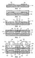
- FIGS. 4-8 there illustrated in cross-sectional form is the sequence of steps in fabricating the sensor 100 of FIG. 1.
- the starting point in the fabrication process is a commercially-available silicon wafer 144 (FIG. 4) that comprises the substrate 108 of a fabricated sensor 100.
- the wafer 144 is appropriately doped with, for example, antimony.
- the substrate wafer 144 may either be doped with either N or P type impurities having a doping concentration of at least 10 15 impurity per cubic centimeter to achieve less than 1 ohm-centimeter resistivity.
- the substrate wafer 144 is etched away at predetermined locations to create a plurality of mesas 136, each mesa 136 being approximately 6.5 microns in height.
- the glass that serves as the dielectric 112 between the diaphragm 104 and the substrate 108 is deposited onto the silicon substrate wafer 144.
- the glass 112 may be deposited onto the wafer 144 using any one of a number of well-known deposition techniques, such as vacuum deposition or sputtering.
- One sputter-deposition technique that may be used to deposit the glass is an ion-milling technique, as described and claimed in copending U.S. patent application entitled "A Silicon Capacitive Pressure Sensor Having A Glass Dielectric Deposited Using Ion Milling", filed December 2, 1993, Serial No. 08/161335, and assigned to the same assignee as the present invention (US-A-5 375 034 published 20.12.94).
- the glass 112 is deposited to a thickness of approximately 9 microns.
- the deposited glass 112 serves three purposes: as a dielectric spacer 112 forming an enclosed vacuum chamber 132 between the conductive substrate 108 and conductive diaphragm 104; as a means of forming a precise gap between the diaphragm 104 and substrate 108; and as an agent for bonding the silicon substrate 108 and diaphragm 104 to the spacer 112.
- the glass 112 comprises the Model 7070 borosilicate glass provided by Corning. This glass 112 has thermal properties (e.g., thermal expansion coefficients) similar to the silicon substrate 108. Also, this specific model of glass 112 has lithium and potassium ions that are available to assist in the bonding of the diaphragm 104 to the glass spacer 112, as described in greater detail hereinafter.
- the glass may comprise other commercially available brands of borosilicate glass, such as Model 7740 borosilicate glass provided by Corning and sold under the trademark PYREX®.
- the glass may comprise, if desired, other types of glass, such as phosphosilicate.
- the type of glass utilized is based in part on the type(s) of alkali contained in the glass.
- the next step in the process of fabricating the silicon capacitive pressure sensor 100 is that the silicon substrate wafer 144 with the glass spacer 112 formed thereon in bulk may be subject to thermal processing, such as annealing, to reduce any stresses in the glass. If desired, the silicon substrate wafer 144 may be subject to a thermal processing procedure described and claimed in copending U.S. Patent Application entitled “Thermal Processing of Deposited Glass", filed December 21, 1993, Docket No. H2324-ED, and assigned to the same assignee as the present invention (no document available).
- Such thermal processing of the glass ensures that any gas particles which are formed inherent in the glass as a result of a sputter-deposition process will diffuse out of the glass, and thus will not contribute to any long-term drift of the sensor. Also, the thermal process ensures that no undesirable and ruinous internal cavities (i.e., "bubbles") will be formed in the glass as a result of other prior art thermal processing procedures.
- the borosilicate glass layer 112 is appropriately etched or patterned (FIG. 6) using well-known photolithography and etching techniques. This forms the pair of concentric glass rings 141, 142 in accordance with the present invention. These patterning techniques also form the glass spacer 112 only around the approximate perimeter of that portion of the silicon substrate wafer 144 that comprises the substrate 108 of the fabricated sensor 100.
- a second silicon wafer 160 may be prepared, by suitable lapping to a desired thickness, such as on the order of 200 microns (i.e., approximately eight mils (0.008")), to form the flexible diaphragm 104 (see FIG. 7).
- the silicon diaphragm wafer 160 may be appropriately doped with the desired impurities.
- the silicon diaphragm wafer 160 is then bonded to the dielectric glass spacer 112 using known electrostatic bonding techniques.
- the diaphragm wafer 160 may be bonded using the known field-assisted sealing technique of joining glass to semiconductors.
- This technique involves subjecting the diaphragm wafer 160 to temperatures of approximately 300-500°C to induce ionic mobility within the borosilicate glass.
- the aforementioned Model 7070 glass from Corning has lithium and potassium ions available at high temperature that may be used in this electrostatic bonding technique.
- the glass spacer and diaphragm junction is then subjected to an electric potential on the order of 100 volts DC. This produces a depletion layer ⁇ at the interface between the silicon and the glass. If the electric potential is properly directed, the positive lithium and potassium ions drift away from the interface and a high field is created across this interface. This causes intimate contact between the glass spacer 112 and the silicon diaphragm wafer 160. In this manner, a hermetic seal between the silicon and glass is formed.
- This above-described process is normally accomplished in a vacuum in order to provide an absolute pressure sensor.
- Both the silicon substrate wafer 144 and silicon diaphragm wafer 160 may have a thin metallization layer deposited locally thereon, for example, a layer of about five thousand angstroms of aluminum. This provides a suitable surface for wire bonding of the electrical wires 140 to both the diaphragm 104 and the substrate 108.
- This silicon wafer comprises the transition piece 116 of a fabricated sensor 100. More particularly, the wafer 164 has the desired transition pieces 116 formed at appropriate locations in the wafer by forming the pedestal-shaped outer surface and the throughbores 124 therein.
- the pedestal shapes and throughbores 124 may be etched in the transition piece silicon wafer 164 using various techniques. For example, the shapes and throughbores 124 may be formed in the transition piece using the electrical discharge machining ("EDM") techniques described and claimed in copending U.S. patent application entitled “Fabricating Complex Silicon Pieces Using Electrical Discharge Machining", filed December 2, 1993, Serial No. 08/161156, and assigned to the same assignee as the present invention.
- the transition piece wafer 164 may be on the order of one hundred twenty-five thousandths (0.125") of an inch thick.
- the transition piece wafer 164 then has a layer 120 of dielectric glass deposited thereon.
- the glass deposited onto the silicon wafer 164 may also comprise the Model 7070 borosilicate glass from Corning.
- the glass layer 120 may be deposited in an identical manner as the glass spacer 112 deposited onto the silicon substrate 108.
- the second glass layer 120 is photolithographically patterned and etched into a ring only around the perimeter of the resulting transition piece 116.
- the glass layer 120 is then bonded to the silicon diaphragm wafer 160 using electrostatic bonding techniques.
- the glass layer 120 contacts the diaphragm wafer 160, as illustrated in FIG. 8.
- the resulting silicon and glass multilayered component is diced appropriately, such as by sawing, to provide a plurality of individual piece parts, as indicated by the phantom lines 168.
- both the silicon substrate 108 and the glass spacer 112 may, if desired, be cut into an octagon shape to expose the electrical connection points on the silicon diaphragm 104.
- the individual piece part silicon capacitive pressure sensor 100 may then be mounted to a surface of the header 128 (FIG. 1).
- the header may comprise a material sold under the trademark KOVAR®, or other similar alloys.
- the header has a ( throughbore 172 that acts as a pressure port through which the fluid whose pressure is desired to be measured by the sensor loo is applied thereto.
- the throughbore 124 of the transition piece 116 is aligned over the pressure port 172 such that the transition piece 116 is in contact with the surface of the header 128.
- the transition piece 116 is then bonded to the header 128 using an eutectic bonding process. This process involves coating with gold the outer surface of the silicon transition piece 116 that is to contact the header 128.
- the sensor 100 and the header 128 are heated at an elevated temperature to bond the sensor 100 to the header 128.
Landscapes
- Physics & Mathematics (AREA)
- General Physics & Mathematics (AREA)
- Measuring Fluid Pressure (AREA)
- Pressure Sensors (AREA)
Abstract
Claims (11)
- Capteur de pression capacitif (100) comprenant un substrat (108), un élément d'écartement diélectrique (112), déposé sur une surface du substrat et un diaphragme (104), fixé à l'élément d'écartement diélectrique, le diaphragme pouvant être fléchi en cas d'application d'une pression de fluide, caractérisé en ce que l'élément d'écartement diélectrique est façonné en une structure prédéterminée comportant un anneau extérieur (142) de forme et d'épaisseur prédéterminées, et un anneau intérieur (141) de forme et d'épaisseur prédéterminées, l'anneau extérieur (142) étant séparé physiquement de l'anneau intérieur d'une distance prédéterminée.
- Capteur de pression capacitif (100) selon la revendication 1, caractérisé en ce que le substrat (108) est composé de silicium, le diaphragme (104) étant composé de silicium et l'élément d'écartement diélectrique (112) étant agencé entre le substrat en silicium et le diaphragme en silicium autour des parties périphériques externes correspondantes pour former une chambre renfermée (132), délimitée par le substrat en silicium, le diaphragme en silicium et l'élément d'écartement diélectrique.
- Capteur de pression capacitif (100) selon les revendications 1 ou 2, caractérisé en ce que le substrat en silicium (108) est plan, le diaphragme en silicium (104) étant plan, le substrat en silicium et le diaphragme en silicium formant les plaques d'un condensateur plan transformant une quelconque flexion du diaphragme en silicium entraínée par l'application de la pression de fluide en une valeur de capacité correspondante, indicative d'une valeur instantanée de la pression du fluide appliquée au diaphragme en silicium.
- Capteur de pression capacitif (100) selon l'une quelconque des revendications 1 à 3, caractérisé en ce que l'élément d'écartement diélectrique (112) comprend du verre.
- Capteur de pression capacitif (100) selon la revendication 4, caractérisé en ce que l'élément d'écartement diélectrique (102) comprend du verre borosilicaté.
- Capteur de pression capacitif (100) selon l'une quelconque des revendications 1 à 5, dans lequel l'élément d'écartement diélectrique (112) est déposé par pulvérisation cathodique sur la surface du substrat (108).
- Capteur de pression capacitif (100) selon l'une quelconque des revendications 1 à 5, caractérisé en ce que le diaphragme (104) est fixé à l'élément d'écartement diélectrique (112) par l'intermédiaire d'un procédé de liaison à effet de champ.
- Capteur de pression capacitif (100) selon l'une quelconque des revendications 1 à 7, caractérisé en ce que la forme prédéterminée de l'anneau extérieur (142) est octogonale.
- Capteur de pression capacitif (100) selon l'une quelconque des revendications 1 à 8, caractérisé en ce que la forme prédéterminée de l'anneau intérieur (141) de l'élément d'écartement est circulaire.
- Capteur de pression capacitif (100) selon l'une quelconque des revendications 1 à 9, caractérisé en ce que le substrat (108) a un périmètre extérieur de forme octogonale.
- Capteur de pression capacitif (100) selon l'une quelconque des revendications 1 à 9, caractérisé en ce que le substrat en silicium (108) a un périmètre extérieur de forme octogonale et en ce que la forme prédéterminée de l'anneau extérieur (142) est octogonale, une surface d'un bord extérieur du substrat en silicium sur chacun des huit côtés du substrat étant coplanaire par rapport à une surface d'un bord extérieur de l'anneau extérieur sur chacun des huit côtés de l'anneau extérieur.
Applications Claiming Priority (3)
| Application Number | Priority Date | Filing Date | Title |
|---|---|---|---|
| US188257 | 1994-01-28 | ||
| US08/188,257 US5448444A (en) | 1994-01-28 | 1994-01-28 | Capacitive pressure sensor having a reduced area dielectric spacer |
| PCT/US1995/001034 WO1995020754A1 (fr) | 1994-01-28 | 1995-01-26 | Capteur de pression capacitif comprenant un element d'ecartement dielectrique a surface reduite |
Publications (2)
| Publication Number | Publication Date |
|---|---|
| EP0742893A1 EP0742893A1 (fr) | 1996-11-20 |
| EP0742893B1 true EP0742893B1 (fr) | 1999-05-19 |
Family
ID=22692406
Family Applications (1)
| Application Number | Title | Priority Date | Filing Date |
|---|---|---|---|
| EP95909337A Expired - Lifetime EP0742893B1 (fr) | 1994-01-28 | 1995-01-26 | Capteur de pression capacitif comprenant un element d'ecartement dielectrique a surface reduite |
Country Status (7)
| Country | Link |
|---|---|
| US (1) | US5448444A (fr) |
| EP (1) | EP0742893B1 (fr) |
| AU (1) | AU1732995A (fr) |
| CA (1) | CA2182180A1 (fr) |
| DE (1) | DE69509751T2 (fr) |
| ES (1) | ES2133739T3 (fr) |
| WO (1) | WO1995020754A1 (fr) |
Families Citing this family (20)
| Publication number | Priority date | Publication date | Assignee | Title |
|---|---|---|---|---|
| GB9425250D0 (en) * | 1994-12-14 | 1995-02-08 | Otter Controls Ltd | Silicon capacitive pressure sensor designed for manufacturability and low long term drift |
| JP3991165B2 (ja) * | 1995-06-20 | 2007-10-17 | 株式会社ニコン | 位置合わせ方法及び露光方法 |
| US5837935A (en) * | 1996-02-26 | 1998-11-17 | Ford Motor Company | Hermetic seal for an electronic component having a secondary chamber |
| US6143583A (en) * | 1998-06-08 | 2000-11-07 | Honeywell, Inc. | Dissolved wafer fabrication process and associated microelectromechanical device having a support substrate with spacing mesas |
| JP2000121469A (ja) * | 1998-10-16 | 2000-04-28 | Mitsubishi Electric Corp | 圧力センサ |
| EP1495491B1 (fr) * | 2002-04-15 | 2020-12-16 | Schott AG | Procédé de liaison de substrats et élément composite |
| US6647794B1 (en) * | 2002-05-06 | 2003-11-18 | Rosemount Inc. | Absolute pressure sensor |
| US6894383B2 (en) * | 2003-03-31 | 2005-05-17 | Intel Corporation | Reduced substrate micro-electro-mechanical systems (MEMS) device and system for producing the same |
| EP1837303A1 (fr) * | 2006-03-24 | 2007-09-26 | Infineon Technologies SensoNor AS | Socle intégré pour monter une structure MEMS |
| US7476289B2 (en) * | 2006-06-29 | 2009-01-13 | Applied Materials, Inc. | Vacuum elastomer bonding apparatus and method |
| US8124953B2 (en) | 2009-03-12 | 2012-02-28 | Infineon Technologies Ag | Sensor device having a porous structure element |
| US7819014B1 (en) * | 2009-04-23 | 2010-10-26 | Rosemount Inc. | Capacitive gage pressure sensor with vacuum dielectric |
| US9146164B2 (en) * | 2013-03-07 | 2015-09-29 | Sensata Technologies, Inc. | Pressure transducer substrate with self alignment feature |
| CN107290099B (zh) | 2016-04-11 | 2021-06-08 | 森萨塔科技公司 | 压力传感器、用于压力传感器的插塞件和制造插塞件的方法 |
| EP3236226B1 (fr) | 2016-04-20 | 2019-07-24 | Sensata Technologies, Inc. | Procédé de fabrication d'un capteur de pression |
| US10545064B2 (en) | 2017-05-04 | 2020-01-28 | Sensata Technologies, Inc. | Integrated pressure and temperature sensor |
| US10323998B2 (en) | 2017-06-30 | 2019-06-18 | Sensata Technologies, Inc. | Fluid pressure sensor |
| US10724907B2 (en) | 2017-07-12 | 2020-07-28 | Sensata Technologies, Inc. | Pressure sensor element with glass barrier material configured for increased capacitive response |
| US10557770B2 (en) | 2017-09-14 | 2020-02-11 | Sensata Technologies, Inc. | Pressure sensor with improved strain gauge |
| US10910500B2 (en) * | 2018-02-13 | 2021-02-02 | Stmicroelectronics S.R.L. | Load sensing devices, packages, and systems |
Citations (2)
| Publication number | Priority date | Publication date | Assignee | Title |
|---|---|---|---|---|
| US4951174A (en) * | 1988-12-30 | 1990-08-21 | United Technologies Corporation | Capacitive pressure sensor with third encircling plate |
| US4954925A (en) * | 1988-12-30 | 1990-09-04 | United Technologies Corporation | Capacitive sensor with minimized dielectric drift |
Family Cites Families (14)
| Publication number | Priority date | Publication date | Assignee | Title |
|---|---|---|---|---|
| US4287553A (en) * | 1980-06-06 | 1981-09-01 | The Bendix Corporation | Capacitive pressure transducer |
| DE3137219A1 (de) * | 1981-09-18 | 1983-04-07 | Robert Bosch Gmbh, 7000 Stuttgart | Kapazitiver drucksensor und verfahren zu seiner herstellung |
| US4405970A (en) * | 1981-10-13 | 1983-09-20 | United Technologies Corporation | Silicon-glass-silicon capacitive pressure transducer |
| US4415948A (en) * | 1981-10-13 | 1983-11-15 | United Technologies Corporation | Electrostatic bonded, silicon capacitive pressure transducer |
| US4467394A (en) * | 1983-08-29 | 1984-08-21 | United Technologies Corporation | Three plate silicon-glass-silicon capacitive pressure transducer |
| US4517622A (en) * | 1983-08-29 | 1985-05-14 | United Technologies Corporation | Capacitive pressure transducer signal conditioning circuit |
| US4513348A (en) * | 1984-01-13 | 1985-04-23 | United Technologies Corporation | Low parasitic capacitance pressure transducer and etch stop method |
| US4530029A (en) * | 1984-03-12 | 1985-07-16 | United Technologies Corporation | Capacitive pressure sensor with low parasitic capacitance |
| US4743836A (en) * | 1985-12-06 | 1988-05-10 | United Technologies Corporation | Capacitive circuit for measuring a parameter having a linear output voltage |
| US4879627A (en) * | 1988-12-30 | 1989-11-07 | United Technologies Corporation | Differential capacitive pressure sensor with over-pressure protection |
| US4883768A (en) * | 1989-02-28 | 1989-11-28 | United Technologies Corporation | Mesa fabrication in semiconductor structures |
| US5044202A (en) * | 1989-09-18 | 1991-09-03 | Texas Instruments Incorporated | Pressure transducer apparatus |
| US5134887A (en) * | 1989-09-22 | 1992-08-04 | Bell Robert L | Pressure sensors |
| JPH03239940A (ja) * | 1990-02-16 | 1991-10-25 | Toyoda Mach Works Ltd | 容量型圧力センサ |
-
1994
- 1994-01-28 US US08/188,257 patent/US5448444A/en not_active Expired - Fee Related
-
1995
- 1995-01-26 AU AU17329/95A patent/AU1732995A/en not_active Abandoned
- 1995-01-26 CA CA002182180A patent/CA2182180A1/fr not_active Abandoned
- 1995-01-26 WO PCT/US1995/001034 patent/WO1995020754A1/fr not_active Ceased
- 1995-01-26 ES ES95909337T patent/ES2133739T3/es not_active Expired - Lifetime
- 1995-01-26 DE DE69509751T patent/DE69509751T2/de not_active Expired - Fee Related
- 1995-01-26 EP EP95909337A patent/EP0742893B1/fr not_active Expired - Lifetime
Patent Citations (2)
| Publication number | Priority date | Publication date | Assignee | Title |
|---|---|---|---|---|
| US4951174A (en) * | 1988-12-30 | 1990-08-21 | United Technologies Corporation | Capacitive pressure sensor with third encircling plate |
| US4954925A (en) * | 1988-12-30 | 1990-09-04 | United Technologies Corporation | Capacitive sensor with minimized dielectric drift |
Also Published As
| Publication number | Publication date |
|---|---|
| US5448444A (en) | 1995-09-05 |
| AU1732995A (en) | 1995-08-15 |
| DE69509751D1 (de) | 1999-06-24 |
| DE69509751T2 (de) | 1999-11-11 |
| ES2133739T3 (es) | 1999-09-16 |
| CA2182180A1 (fr) | 1995-08-03 |
| WO1995020754A1 (fr) | 1995-08-03 |
| EP0742893A1 (fr) | 1996-11-20 |
Similar Documents
| Publication | Publication Date | Title |
|---|---|---|
| US5381299A (en) | Capacitive pressure sensor having a substrate with a curved mesa | |
| EP0742893B1 (fr) | Capteur de pression capacitif comprenant un element d'ecartement dielectrique a surface reduite | |
| JP2517467B2 (ja) | 静電容量式圧力センサ | |
| JP3114570B2 (ja) | 静電容量型圧力センサ | |
| KR0137939B1 (ko) | 용량성 압력감지기 및 그의 기생용량 최소화 방법 | |
| US4405970A (en) | Silicon-glass-silicon capacitive pressure transducer | |
| US4609966A (en) | Absolute pressure transducer | |
| JP3444639B2 (ja) | 一体型圧力変換器の製造方法および装置 | |
| US8384170B2 (en) | Pressure sensor | |
| KR0137965B1 (ko) | 최소의 유전 표류를 가지는 용량성 감지기 | |
| US4531267A (en) | Method for forming a pressure sensor | |
| US4445384A (en) | Piezoelectric pressure sensor | |
| EP0376631A1 (fr) | Capteur capacitif de pression différentielle avec protection contre la surpression et procédé pour la protection d'un capteur de pression capacitif contre la surpression | |
| JPH0623782B2 (ja) | 静電容量式加速度センサ及び半導体圧力センサ | |
| JPH0750789B2 (ja) | 半導体圧力変換装置の製造方法 | |
| EP0385574A1 (fr) | Capteur capacitif à semi-conducteur avec diaphragme articulé pour mouvement plan | |
| EP0633459B1 (fr) | Transducteur de pression capacitif et son procédé de fabrication | |
| JPH06129933A (ja) | 過圧保護ポリシリコン容量性差圧センサー及びその製造方法 | |
| US5317922A (en) | Capacitance transducer article and method of fabrication | |
| US5444901A (en) | Method of manufacturing silicon pressure sensor having dual elements simultaneously mounted | |
| US5440931A (en) | Reference element for high accuracy silicon capacitive pressure sensor | |
| CA1154502A (fr) | Transducteur de pression a capacite variable a semiconducteur | |
| JPH05340832A (ja) | 圧力マイクロセンサ | |
| US5744725A (en) | Capacitive pressure sensor and method of fabricating same | |
| US5375034A (en) | Silicon capacitive pressure sensor having a glass dielectric deposited using ion milling |
Legal Events
| Date | Code | Title | Description |
|---|---|---|---|
| PUAI | Public reference made under article 153(3) epc to a published international application that has entered the european phase |
Free format text: ORIGINAL CODE: 0009012 |
|
| 17P | Request for examination filed |
Effective date: 19960705 |
|
| AK | Designated contracting states |
Kind code of ref document: A1 Designated state(s): DE ES FR GB IT SE |
|
| 17Q | First examination report despatched |
Effective date: 19980723 |
|
| GRAG | Despatch of communication of intention to grant |
Free format text: ORIGINAL CODE: EPIDOS AGRA |
|
| GRAG | Despatch of communication of intention to grant |
Free format text: ORIGINAL CODE: EPIDOS AGRA |
|
| GRAH | Despatch of communication of intention to grant a patent |
Free format text: ORIGINAL CODE: EPIDOS IGRA |
|
| GRAH | Despatch of communication of intention to grant a patent |
Free format text: ORIGINAL CODE: EPIDOS IGRA |
|
| GRAA | (expected) grant |
Free format text: ORIGINAL CODE: 0009210 |
|
| AK | Designated contracting states |
Kind code of ref document: B1 Designated state(s): DE ES FR GB IT SE |
|
| PG25 | Lapsed in a contracting state [announced via postgrant information from national office to epo] |
Ref country code: IT Free format text: LAPSE BECAUSE OF FAILURE TO SUBMIT A TRANSLATION OF THE DESCRIPTION OR TO PAY THE FEE WITHIN THE PRESCRIBED TIME-LIMIT;WARNING: LAPSES OF ITALIAN PATENTS WITH EFFECTIVE DATE BEFORE 2007 MAY HAVE OCCURRED AT ANY TIME BEFORE 2007. THE CORRECT EFFECTIVE DATE MAY BE DIFFERENT FROM THE ONE RECORDED. Effective date: 19990519 |
|
| REF | Corresponds to: |
Ref document number: 69509751 Country of ref document: DE Date of ref document: 19990624 |
|
| ET | Fr: translation filed | ||
| REG | Reference to a national code |
Ref country code: ES Ref legal event code: FG2A Ref document number: 2133739 Country of ref document: ES Kind code of ref document: T3 |
|
| PLBE | No opposition filed within time limit |
Free format text: ORIGINAL CODE: 0009261 |
|
| STAA | Information on the status of an ep patent application or granted ep patent |
Free format text: STATUS: NO OPPOSITION FILED WITHIN TIME LIMIT |
|
| 26N | No opposition filed | ||
| REG | Reference to a national code |
Ref country code: GB Ref legal event code: IF02 |
|
| PGFP | Annual fee paid to national office [announced via postgrant information from national office to epo] |
Ref country code: FR Payment date: 20021230 Year of fee payment: 9 |
|
| PGFP | Annual fee paid to national office [announced via postgrant information from national office to epo] |
Ref country code: GB Payment date: 20030106 Year of fee payment: 9 |
|
| PGFP | Annual fee paid to national office [announced via postgrant information from national office to epo] |
Ref country code: SE Payment date: 20030117 Year of fee payment: 9 |
|
| PGFP | Annual fee paid to national office [announced via postgrant information from national office to epo] |
Ref country code: ES Payment date: 20030124 Year of fee payment: 9 |
|
| REG | Reference to a national code |
Ref country code: GB Ref legal event code: 732E |
|
| PG25 | Lapsed in a contracting state [announced via postgrant information from national office to epo] |
Ref country code: GB Free format text: LAPSE BECAUSE OF NON-PAYMENT OF DUE FEES Effective date: 20040126 |
|
| PG25 | Lapsed in a contracting state [announced via postgrant information from national office to epo] |
Ref country code: SE Free format text: LAPSE BECAUSE OF NON-PAYMENT OF DUE FEES Effective date: 20040127 Ref country code: ES Free format text: LAPSE BECAUSE OF NON-PAYMENT OF DUE FEES Effective date: 20040127 |
|
| EUG | Se: european patent has lapsed | ||
| GBPC | Gb: european patent ceased through non-payment of renewal fee |
Effective date: 20040126 |
|
| PG25 | Lapsed in a contracting state [announced via postgrant information from national office to epo] |
Ref country code: FR Free format text: LAPSE BECAUSE OF NON-PAYMENT OF DUE FEES Effective date: 20040930 |
|
| REG | Reference to a national code |
Ref country code: FR Ref legal event code: ST |
|
| PGFP | Annual fee paid to national office [announced via postgrant information from national office to epo] |
Ref country code: DE Payment date: 20050128 Year of fee payment: 11 |
|
| REG | Reference to a national code |
Ref country code: ES Ref legal event code: FD2A Effective date: 20040127 |
|
| PG25 | Lapsed in a contracting state [announced via postgrant information from national office to epo] |
Ref country code: DE Free format text: LAPSE BECAUSE OF NON-PAYMENT OF DUE FEES Effective date: 20060801 |