EP0737308B1 - Optical sensor for detection of chemical species - Google Patents
Optical sensor for detection of chemical species Download PDFInfo
- Publication number
- EP0737308B1 EP0737308B1 EP19940919591 EP94919591A EP0737308B1 EP 0737308 B1 EP0737308 B1 EP 0737308B1 EP 19940919591 EP19940919591 EP 19940919591 EP 94919591 A EP94919591 A EP 94919591A EP 0737308 B1 EP0737308 B1 EP 0737308B1
- Authority
- EP
- European Patent Office
- Prior art keywords
- light
- chemical species
- thickness
- guiding
- optical sensor
- Prior art date
- Legal status (The legal status is an assumption and is not a legal conclusion. Google has not performed a legal analysis and makes no representation as to the accuracy of the status listed.)
- Expired - Lifetime
Links
Images


Classifications
-
- G—PHYSICS
- G01—MEASURING; TESTING
- G01N—INVESTIGATING OR ANALYSING MATERIALS BY DETERMINING THEIR CHEMICAL OR PHYSICAL PROPERTIES
- G01N21/00—Investigating or analysing materials by the use of optical means, i.e. using sub-millimetre waves, infrared, visible or ultraviolet light
- G01N21/75—Systems in which material is subjected to a chemical reaction, the progress or the result of the reaction being investigated
- G01N21/77—Systems in which material is subjected to a chemical reaction, the progress or the result of the reaction being investigated by observing the effect on a chemical indicator
- G01N21/7703—Systems in which material is subjected to a chemical reaction, the progress or the result of the reaction being investigated by observing the effect on a chemical indicator using reagent-clad optical fibres or optical waveguides
-
- G—PHYSICS
- G01—MEASURING; TESTING
- G01N—INVESTIGATING OR ANALYSING MATERIALS BY DETERMINING THEIR CHEMICAL OR PHYSICAL PROPERTIES
- G01N21/00—Investigating or analysing materials by the use of optical means, i.e. using sub-millimetre waves, infrared, visible or ultraviolet light
- G01N21/75—Systems in which material is subjected to a chemical reaction, the progress or the result of the reaction being investigated
- G01N21/77—Systems in which material is subjected to a chemical reaction, the progress or the result of the reaction being investigated by observing the effect on a chemical indicator
- G01N2021/7769—Measurement method of reaction-produced change in sensor
- G01N2021/7776—Index
Definitions
- This invention relates to an optical sensor useful for detecting, quantifying or differentiating chemical species in gaseous or liquid states, as well as an apparatus for detecting chemical species using said optical sensor.
- the measurement system under consideration utilizes the effect that the thickness and refractive index of an optical waveguide change upon adsorption of biochemical molecules on top of the waveguide. Such changes can be detected by measuring the coupling angle in the case where a grating coupler or a prism coupler is used. This detection corresponds to the measurement of effective refractive index of certain modes.
- the conventional sensors described above utilize the swelling of thin polymer films and detect it by various methods, including interference enhanced reflection (IER) and surface plasmon resonance for measuring the changes in the thickness or refractive index of the thin polymer film.
- IER interference enhanced reflection
- surface plasmon resonance for measuring the changes in the thickness or refractive index of the thin polymer film.
- US-A-4,270,049 discloses a liquid leakage detection system for the detection of the leakage of a liquid in terms of the drop of intensity of light rays travelling through a light guide core or optical fiber made of glass or synthetic resin due to the adhesion of the leaked liquid to the light guide.
- EP-A-0 584 005 discloses an optical collector which comprises a parallel double-spiralled interleaved waveguides integrated on a substrate.
- a signal from a light source passes through a fork coupler to separate the source light into two paths.
- the output signal is sent to a detector through a second coupler.
- One guide forms a reference isolated from the substance being measured, and the second measuring guide is affected by the substance.
- the entrances and exits to the spiral are placed on the same side of the substrate.
- EP-A-0 481 440 discloses a sensor which consists of an integrated optical interferometer with a measurement arm and a comparison arm in a waveguide substrate.
- EP-A-0 487 992 discloses an optical sensor for liquid or gaseous media which has an integrated optical device, especially an interferometer, for measuring the optical absorption coefficient and refractive index with waveguide(s).
- Another object of the invention is to measure the attenuation of light in a certain mode travelling through an optical waveguide.
- a further object of the invention is to provide a sensor capable of distinguishing between different chemical species.
- a still further object of the invention is to provide an array of optical sensor elements made of the same or different materials for improving the identifiability of chemical species to be detected, correcting for background effects or simultaneously detecting different chemical species.
- Yet another object of the invention is to provide a detection system that comprises a light source, a waveguide, couplers for coupling light in and out of the waveguide, and a photodetector to measure the intensity of light.
- an optical sensor for the detection of chemical species comprising a planar optical waveguide having a guiding thin film (3), wherein the thickness and optionally the refractive index of said guiding thin film (3) changes due to the adsorption or absorption of chemical species or the reaction with the same characterized in that the thickness of said guiding thin film (3) is above the cutoff thickness in presence of gaseous or liquid chemical species to be detected and the thickness is below the cutoff thickness in the absence of such chemical species.
- the present invention which comprises an optical sensor for measuring the attenuation of light for certain modes in an optical waveguide.
- the invention utilizes the fact that the attenuation of light in certain modes originates from the changes in the thickness and/or refractive index of a guiding thin film.
- the guiding thin film interacts with the chemical species to be detected, whereby the thickness and/or refractive index of the film will change.
- the guiding characteristics of the optical waveguide namely, the degree of attenuation of light in a certain mode, will change.
- the degree of attenuation of light in a given mode can be known by exciting light for the given mode and then measuring either the intensity of light coupled out of the optical waveguide or the intensity of light that could be launched into the waveguide (i.e., the difference between the intensities of incident light and reflected light as measured at the coupler on the entrance side). Therefore, the use of special parts such as a birefringent film is essentially unnecessary for the present invention.
- the measured intensity of light is proportional to the concentration of the chemical species to be detected over a certain range, so according to the invention, not only can the chemical species of interest be detected for its presence but its concentration can also be measured.
- the optical sensor of the present invention for the detection of chemical species comprises a planar optical waveguide having a guiding thin film (3), wherein the thickness and optionally the refractive index of said guiding thin film (3) changes due to the adsorption or absorption of chemical species or the reaction with the same characterized in that the thickness of said guiding thin film (3) is above the cutoff thickness in presence of gaseous or liquid chemical species to be detected and the thickness is below the cutoff thickness in the absence of such chemical species.
- Said optical sensor includes couplers disposed on the optical waveguide for coupling light in and out of said waveguide.
- the chemical species to be detected is adsorbed to or absorbed by the guiding thin film or it reacts with the latter, whereby the thickness or refractive index of the thin film and, hence, its guiding characteristics will change.
- the mode of light will change from a guiding mode to a radiating mode or vice versa, whereby the intensity of light travelling through the waveguide varies.
- the guiding thin film must be transparent. The change from the guiding to the radiating mode accompanies the decrease in the thickness of the guiding film. In other words, there exists a minimum thickness for the guiding thin film to maintain the guiding mode and this minimum thickness shall hereunder be referred to as the "cutoff thickness".
- the guiding characteristics of light for certain modes in the optical waveguide are determined by the thickness and/or refractive index of the guiding film.
- the thickness of the film varies with the concentration of the chemical species of interest in contact with the surface of the film and the guiding characteristics of light will change accordingly.
- the thickness of the guiding film is selected at such a value that light in a certain of various modes can be guided through the film in a "wet" state (i.e., the guiding mode) but not through the film in a "dry” state (i.e., the radiating mode).
- the guiding film is required to be thicker than the cutoff thickness in the "wet” state but thinner than the cutoff thickness in the "dry” state.
- the "wet” state means the state of the guiding thin film in the presence of the gaseous or liquid chemical species to be detected whereas the “dry” state refers to the state of the film in the absence of such chemical species. It should also be noted that the terms “wet” and “dry” correspond to large and small thicknesses, respectively, of the guiding film, or correspond to high and low refractive indices, respectively, of the film.
- the guiding film in the wet state is thicker than the cutoff thickness and hence is capable of guiding light (in the guiding mode); however, in the dry state, the film is thinner than the cutoff thickness and it is in the radiating mode, in which light radiates its energy outside the film so that its intensity becomes very low at the exit end of the optical waveguide.
- the optical sensor of the invention is capable of differential detection of two or more chemical species by making use of the difference in the intensity of outgoing light and/or the response characteristics based on those differences in the interaction.
- the guiding thin film to be used in the invention may be of any kind as long as it is capable of reacting with or absorbing or adsorbing one or more chemical species to be detected.
- the film can be advantageously prepared from organic or polymeric materials.
- the polymeric materials that can be used to make the guiding thin film include vinyl polymers having different side-chain groups, polysiloxanes, polycondensates such as polyesters, polyamides, polyimides, polyurethanes and polyureas.
- organic materials of low molecular weights include phthalocyanines, porphins, porphyrins, organometallic complexes, complexing agents such as cyclodextrins, calixarenes, crown ethers and other crown compounds (e.g., aza crowns) and cryptands.
- the substrate for supporting the guiding thin film may be of any kind as long as it is flat. In order to guide light through the film, it must be surrounded by a cladding that is made of a material having a lower refractive index. If the substrate has a lower refractive index than the guiding film, the latter can be directly applied onto the substrate without using claddings.
- the surface of the guiding film on the side that is not in contact with the substrate may contact either air or, depending on the use, it may be overlaid with a cover layer for protecting the thin film or a superstrate as a cladding. In ordinary cases, the air layer adjacent the guiding thin film will serve as the superstrate.
- a SiO 2 layer may be provided between the Si substrate and a thin organic or polymeric layer.
- the guiding thin film can be formed from the above-mentioned materials by any of the known thin-film forming techniques including spin coating, polymer solution casting, melt extrusion and vapor-phase deposition.
- the invention encompasses the use of an array of optical sensor elements for detecting chemical species. Stated more specifically, a plurality of units of the optical sensor described hereinabove are assembled to make an optical sensor array.
- the guiding thin films and/or substrates may be of the same or different kinds in the individual planar optical waveguides.
- the array of optical sensor elements enables different chemical species to be detected and/or identified simultaneously.
- the present invention also provides an apparatus for detecting chemical species comprising the sensor itself (including couplers for coupling light in or out of the optical waveguide), a light source for launching light into the sensor, a photodetector for detecting the intensity of incident light and/or emerging light, and a peripheral electric circuit.
- Useful light sources include a semiconductor, a solid laser such as a Nd:YAG laser, a gas laser such as a He-Ne laser, a dye laser, a light-emitting diode, etc.
- Any couplers can be used as long as they are capable of coupling light into or out of the planar optical waveguide, as exemplified by a prism coupler, a grating coupler and a fiber optical coupler.
- the photodetector is used to measure the intensity of the incident light and/or the intensity of light emerging from the planar optical waveguide and may be exemplified by a photodiode, a phototransistor, a photoconductor, a photoelectric tube, a photomultiplier tube and other devices that are capable of converting the intensity of light to electric signals.
- the peripheral electric circuit has means for processing and amplifying the electric signals from the photodetector and outputting the result to a recorder.
- the peripheral electric circuit may also include means such as an alarm for signaling the presence of hazardous substances such as toxic, burnables or flammables substances as detected by the sensor, and/or means for isolating those substances, for example, means for turning on or off switches or pipelines.
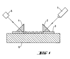
- FIG. 1 An embodiment of the apparatus of the invention for detecting chemical species is shown in Fig. 1.
- Light from a light source 1 is coupled to a planar optical waveguide via a prism coupler 2. If the light emitted from the light source is not polarized, it is desirably polarized by a suitable polarizer such as a polarizing plate.
- the planar optical waveguide comprises a guiding thin film 3 and a substrate 6. If desired, a cladding may be provided between the thin film 3 and the substrate 6. The incident light travels through the guiding thin film 3 and emerges therefrom as it is coupled by another prism coupler 4 and the intensity of the outgoing light is measured with a photodetector 5.
- the two prism couplers are adjusted for their coupling angle in such a manner that light for a certain mode will be excited in the planar optical waveguide.
- the two prism couplers are typically spaced apart by a distance of about 1 to 100 mm.
- the chemical species to be detected will flow over the guiding thin film 3 between the two prism couplers.
- the thickness of the guiding film depends on various parameters including the kind of the chemical species to be detected, the kind of the material which constitutes the film, the mode of light being guided and/or the kind of the substrate to be used; the thickness of the film ranges typically from about 0.1 to 100 ⁇ m, preferably from 0.5 to 10 ⁇ m.
- the interaction between the two i.e., adsorption, absorption or reaction
- the interaction between the two i.e., adsorption, absorption or reaction
- This causes a change in the intensity of outgoing light, which is measured as a change in the signal from the photodetector. This is how one can determine whether the chemical species to be detected is present in the gas or liquid under analysis.
- the intensity of outgoing light is proportional to the concentration of the chemical species of interest over a certain range and this fact may be used to enable the quantitation of the chemical species.
- chemical species having various concentrations are allowed to pass over the optical sensor in the apparatus of the invention and the intensity of light is measured for each passage, thereby establishing a calibration curve to express the relationship between concentration and light intensity.
- Another way to measure the attenuation of light in a certain mode is to excite the light that is coupled to the planar optical waveguide by means of the coupler and then measure the intensity of light emerging from the planar waveguide.
- a beam splitter may be used to split the light from the light source in the present invention.
- a portion of the thus split light is used as reference light while the other portion is coupled via the coupler to the optical waveguide.
- two photodetectors are used, one for measuring the intensity of the reference light and the other for measuring the intensity of light emerging from the planar waveguide.
- the final output will be expressed as the intensity ratio between the light emerging from the planar waveguide and the reference light. This procedure can be omitted if the intensity of the light from the light source is reasonably stable.
- the couplers In the case where light is to be guided in several different modes through the planar waveguide, the couplers must have means capable of distinguishing between the modes of light to be coupled. If prism or grating couplers are to be used, the resonance condition for the excitation of light in a certain mode depends on the coupling angle of the light. Therefore, the intensities of light in various modes can easily be distinguished by measuring the intensity of light at different coupling angles.
- the invention encompasses the use of suitable optical members for splitting, guiding, focusing or collimating the light to the optical waveguide and/or photodetector.
- the optical sensor of the invention is capable of detecting chemical species irrespective of whether it is gaseous or liquid. Further, the sensor has an extremely high sensitivity, wide dynamic range and high response speed. Yet, the sensor uses only of inexpensive components.
- the optical sensor of the invention is applicable to various fields including process control, quality control and the detection of gas or liquid leakage. A particularly advantageous application of the sensor is where high-sensitivity performance and low cost are required, as exemplified by environmental monitoring for measuring the pollution of air or water. It should also be mentioned that the sensor of the invention is inherently explosion proof and can even be used in environments involving the risk of explosion.
- the cutoff value for the thickness of a guiding thin film was determined in this example.
- a ZnO substrate was overlaid with a guiding thin sapphire film to prepare an optical waveguide.
- Fig. 2 plots the velocity of light in TE and TM modes versus the thickness of the guiding film.
- the wavelength of the light was 632.8 nm.
- n eff denotes the effective refractive index of light in the TE or TM modes
- ⁇ refers to the propagation constant
- n 2 designates the refractive index of sapphire
- n 3 represents the refractive index of the ZnO substrate.
- the cutoff thickness of the guiding film exists for each mode of light and light of neither mode will be guided below the cutoff thickness.
- relevant parameters such as the refractive indices of the guiding thin film, the substrate, the cover layer and the superstrate (if present)
- the value of the cutoff thickness can be calculated from equations (13.2-5) and (13.2-11) in A. Yariv, "Optical Electronics", Saunders College Publishing, 1991, International Edition.
- the experimental setup comprised a laser diode emitting at a wavelength ( ⁇ ) of 670 nm (ILEE LDA2000), a 30-mm focusing lens, two prism couplers for coupling light into and out of the optical waveguide, and a photodetector available from Anritsu Corp., Tokyo, Japan.
- the two prism couplers were spaced apart by a distance of about 10 mm.
- the whole setup was put in a chamber in which values of temperature and humidity are controlled.
- a 1:1 copolymer of 2-ethylhexyl methacrylate and styrene was dissolved in cyclohexanone and the solution was spin coated onto a slide glass to construct an optical waveguide.
- the guiding film had a thickness close to the cutoff value for TE 1 mode. In the dry state, the guiding film was too thin to guide light in the TE 1 mode. The thickness of the film increased gradually with the increasing humidity in air. The thus swollen film was capable of guiding light in the TE 1 mode. Thus, humidity could be measured over a wide range.
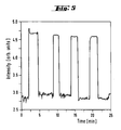
- Fig. 3 the intensity of light as measured with a photodetector and as indicated by a solid line is contrasted with the humidity in the chamber as indicated by a dashed line. Obviously, the two curves are almost identical in shape, demonstrating that the intensity of light is proportional to the humidity in air.
- Fig. 4 shows the time response of the sensor used in Example 2.
- the humidity in the chamber was dropped from 60% to 30%, then raised to 60% again, the intensity of light followed the changes in humidity almost immediately. It took about three seconds for the light intensity to reach the value corresponding to the initial humidity at 60%. This time lag would probably be caused by the time necessary for dry air to replace wet air, not by the inherent time response of the sensor.
- Example 3 gasoline detection was made using the same experimental setup as in Example 2. The result is shown in Fig. 5.
- dry air 0% gasoline
- gasoline saturated air were permitted to flow over the optical sensor cyclically, the intensity of light varied accordingly in the same way.
- the sensor used in Example 3 had a very fast response time of only a few seconds.
Applications Claiming Priority (3)
| Application Number | Priority Date | Filing Date | Title |
|---|---|---|---|
| JP13197593A JP3157952B2 (ja) | 1993-06-02 | 1993-06-02 | 化学物質検出用光学センサー |
| JP131975/93 | 1993-06-02 | ||
| PCT/EP1994/001768 WO1994028395A1 (en) | 1993-06-02 | 1994-05-31 | Optical sensor for detection of chemical species |
Publications (2)
| Publication Number | Publication Date |
|---|---|
| EP0737308A1 EP0737308A1 (en) | 1996-10-16 |
| EP0737308B1 true EP0737308B1 (en) | 1998-03-11 |
Family
ID=15070610
Family Applications (1)
| Application Number | Title | Priority Date | Filing Date |
|---|---|---|---|
| EP19940919591 Expired - Lifetime EP0737308B1 (en) | 1993-06-02 | 1994-05-31 | Optical sensor for detection of chemical species |
Country Status (5)
| Country | Link |
|---|---|
| US (1) | US5640234A (ja) |
| EP (1) | EP0737308B1 (ja) |
| JP (1) | JP3157952B2 (ja) |
| DE (1) | DE69409009T2 (ja) |
| WO (1) | WO1994028395A1 (ja) |
Cited By (10)
| Publication number | Priority date | Publication date | Assignee | Title |
|---|---|---|---|---|
| US7951583B2 (en) | 2006-03-10 | 2011-05-31 | Plc Diagnostics, Inc. | Optical scanning system |
| CN102033042B (zh) * | 2009-09-28 | 2012-08-22 | 中国科学院电子学研究所 | 光波导生化传感器测试装置 |
| US8288157B2 (en) | 2007-09-12 | 2012-10-16 | Plc Diagnostics, Inc. | Waveguide-based optical scanning systems |
| US8675199B2 (en) | 2006-03-10 | 2014-03-18 | Plc Diagnostics, Inc. | Waveguide-based detection system with scanning light source |
| US8747751B2 (en) | 2008-06-16 | 2014-06-10 | Plc Diagnostics, Inc. | System and method for nucleic acids sequencing by phased synthesis |
| US9423397B2 (en) | 2006-03-10 | 2016-08-23 | Indx Lifecare, Inc. | Waveguide-based detection system with scanning light source |
| US9528939B2 (en) | 2006-03-10 | 2016-12-27 | Indx Lifecare, Inc. | Waveguide-based optical scanning systems |
| US9976192B2 (en) | 2006-03-10 | 2018-05-22 | Ldip, Llc | Waveguide-based detection system with scanning light source |
| US10018566B2 (en) | 2014-02-28 | 2018-07-10 | Ldip, Llc | Partially encapsulated waveguide based sensing chips, systems and methods of use |
| US11181479B2 (en) | 2015-02-27 | 2021-11-23 | Ldip, Llc | Waveguide-based detection system with scanning light source |
Families Citing this family (39)
| Publication number | Priority date | Publication date | Assignee | Title |
|---|---|---|---|---|
| EP0725269A3 (en) * | 1995-02-03 | 1997-12-17 | Motorola, Inc. | Optical sensor and method therefor |
| DE19521628A1 (de) * | 1995-06-14 | 1997-01-09 | Hoechst Ag | Optische Sonde mit Sensor aus einem optischen Polymeren |
| US5724151A (en) * | 1995-08-04 | 1998-03-03 | E.I. Du Pont De Nemours And Company | Waveguide sensing element for use in a sample medium and method of rear-firing electromagnetic radiation |
| US5739537A (en) * | 1995-12-21 | 1998-04-14 | Perstorp Analytical, Inc. | NIR absorbance measuring instrument with ATR probe |
| JP3343321B2 (ja) * | 1996-04-18 | 2002-11-11 | アヴェンティス・リサーチ・ウント・テクノロジーズ・ゲーエムベーハー・ウント・コー・カーゲー | 給油機 |
| EP0834735A3 (en) * | 1996-10-01 | 1999-08-11 | Texas Instruments Inc. | A sensor |
| US6224830B1 (en) * | 1998-01-30 | 2001-05-01 | The Governors Of The University Of Alberta | Absorbance cell for microfluid devices |
| EP2360271A1 (en) | 1998-06-24 | 2011-08-24 | Illumina, Inc. | Decoding of array sensors with microspheres |
| DE19839552C2 (de) * | 1998-08-31 | 2001-07-05 | Siemens Ag | Optischer Sensor zur Erkennung einer Konzentration von Ionen, Atomen und/oder Molekülen in einem zu überwachenden Medium |
| ATE366414T1 (de) | 1998-11-13 | 2007-07-15 | Reichert Inc | Verfahren für qualitative und quantitative messungen |
| DE10030927C1 (de) * | 2000-06-24 | 2002-05-23 | Glukomeditech Ag | Refraktometrisches Verfahren zur langzeitstabilen genauen Messung der Konzentrationen gelöster Stoffe sowie eine miniaturisierbare Vorrichtung zu seiner Durchführung |
| US6594420B1 (en) * | 2000-07-28 | 2003-07-15 | Harris Corporation | Multi-fiber ribbon form factor-compliant, integrated multi-channel optical amplifier |
| US6694067B1 (en) * | 2001-01-05 | 2004-02-17 | Los Gatos Research | Cavity enhanced fiber optic and waveguide chemical sensor |
| US6646747B2 (en) * | 2001-05-17 | 2003-11-11 | Sioptical, Inc. | Interferometer apparatus and associated method |
| GB0117230D0 (en) * | 2001-07-14 | 2001-09-05 | Marconi Applied Technologies | Detecting analytes |
| US20040063220A1 (en) * | 2002-02-27 | 2004-04-01 | Lebrun Stewart J. | Substrate chemistry for protein immobilization on a rigid support |
| US20050054118A1 (en) * | 2002-02-27 | 2005-03-10 | Lebrun Stewart J. | High throughput screening method |
| US6763698B2 (en) | 2002-03-15 | 2004-07-20 | Battelle Memorial Institute | Self calibrating system and technique for ultrasonic determination of fluid properties |
| US7395711B2 (en) * | 2002-05-06 | 2008-07-08 | Battelle Memorial Institute | System and technique for characterizing fluids using ultrasonic diffraction grating spectroscopy |
| US6877375B2 (en) * | 2002-05-06 | 2005-04-12 | Battelle Memorial Institute | System and technique for characterizing fluids using ultrasonic diffraction grating spectroscopy |
| US20040072274A1 (en) * | 2002-05-09 | 2004-04-15 | Lebrun Stewart J. | System and method for visualization and digital analysis of protein and other macromolecule microarrays |
| WO2004065000A1 (en) * | 2003-01-21 | 2004-08-05 | Illumina Inc. | Chemical reaction monitor |
| US20060127963A1 (en) * | 2003-11-21 | 2006-06-15 | Lebrun Stewart J | Microarray-based analysis of rheumatoid arthritis markers |
| US20050124017A1 (en) * | 2003-12-05 | 2005-06-09 | Stewart Lebrun | Quantitative alkaline-phosphatase precipitation reagent and methods for visualization of protein microarrays |
| FR2871573B1 (fr) * | 2004-06-11 | 2007-03-30 | Cybernetix Sa | Detecteur et procede de detection optique et electrique d'au moins un gaz determine dans une atmosphere ambiante |
| FR2871571B1 (fr) * | 2004-06-11 | 2007-03-16 | Cybernetix Sa | Procede de detecton et detecteur optique de gaz |
| JP4811757B2 (ja) * | 2004-09-30 | 2011-11-09 | 独立行政法人産業技術総合研究所 | メソポーラス金属酸化物複合光導波路センサー、その製造方法及びそれを用いたガスセンサー |
| US7271914B2 (en) * | 2005-02-02 | 2007-09-18 | National Taiwan University | Biomolecular sensor system utilizing a transverse propagation wave of surface plasmon resonance (SPR) |
| DE102005055288A1 (de) * | 2005-10-17 | 2007-04-19 | Universität Duisburg-Essen | Sensor und Verfahren zur optischen Detektion eines chemischen Stoffs |
| US7842243B2 (en) * | 2006-02-21 | 2010-11-30 | Sergey Sergeyevich Sarkisov | Chemical sensor with an indicator dye |
| US20090103099A1 (en) * | 2006-04-19 | 2009-04-23 | Interuniversitair Microelektronica Centrum | Integrated surface mode biosensor |
| US7403673B2 (en) * | 2006-05-19 | 2008-07-22 | Institut National D'optional | Optical fiber polarimetric chemical sensor |
| US20080158563A1 (en) * | 2006-08-21 | 2008-07-03 | Pierre Simon Joseph Berini | Sensors |
| JP2010197046A (ja) * | 2007-05-28 | 2010-09-09 | Tanaka Holdings Kk | バイオセンサー |
| US20090116021A1 (en) * | 2007-10-05 | 2009-05-07 | Jeffry Mark Bulson | Method and apparatus for determining composition and concentration of contaminants on a film encapsulated in a plasma display panel |
| US20100003764A1 (en) * | 2008-07-02 | 2010-01-07 | Anastasios Angelopoulos | Optical sensor |
| US10599764B2 (en) | 2015-11-02 | 2020-03-24 | Microsoft Technology Licensing, Llc | Operations on images associated with cells in spreadsheets |
| TWI565941B (zh) * | 2016-01-07 | 2017-01-11 | 國立交通大學 | 光學量測系統及其濃度感測裝置 |
| US10433387B2 (en) * | 2016-12-28 | 2019-10-01 | Asahi Kasei Microdevices Corporation | Light emitting device and light emitting and receiving device |
Family Cites Families (9)
| Publication number | Priority date | Publication date | Assignee | Title |
|---|---|---|---|---|
| CA1154117A (en) * | 1978-06-12 | 1983-09-20 | Masaya Tanaka | Liquid leakage detection system |
| US4373768A (en) * | 1980-03-31 | 1983-02-15 | Raychem Corporation | Thermostatic fiber optic waveguides |
| US5120131A (en) * | 1988-02-14 | 1992-06-09 | Walter Lukosz | Method and apparatus for selecting detection of changes in samples by integrated optical interference |
| US5082629A (en) * | 1989-12-29 | 1992-01-21 | The Board Of The University Of Washington | Thin-film spectroscopic sensor |
| DE4033357A1 (de) * | 1990-10-19 | 1992-04-23 | Iot Entwicklungsgesellschaft F | Sensor zum stoffnachweis |
| DE4037431A1 (de) * | 1990-11-24 | 1992-05-27 | Fraunhofer Ges Forschung | Optischer sensor |
| JPH0785122B2 (ja) * | 1991-07-10 | 1995-09-13 | 有限会社旭製作所 | 光ファイバセンサ |
| FR2694630B1 (fr) * | 1992-08-10 | 1994-09-09 | Commissariat Energie Atomique | Capteur en optique intégrée, notamment pour substances chimiques. |
| US5513913A (en) * | 1993-01-29 | 1996-05-07 | United Technologies Corporation | Active multipoint fiber laser sensor |
-
1993
- 1993-06-02 JP JP13197593A patent/JP3157952B2/ja not_active Expired - Fee Related
-
1994
- 1994-05-31 WO PCT/EP1994/001768 patent/WO1994028395A1/en active IP Right Grant
- 1994-05-31 DE DE1994609009 patent/DE69409009T2/de not_active Expired - Lifetime
- 1994-05-31 US US08/545,631 patent/US5640234A/en not_active Expired - Lifetime
- 1994-05-31 EP EP19940919591 patent/EP0737308B1/en not_active Expired - Lifetime
Cited By (13)
| Publication number | Priority date | Publication date | Assignee | Title |
|---|---|---|---|---|
| US9976192B2 (en) | 2006-03-10 | 2018-05-22 | Ldip, Llc | Waveguide-based detection system with scanning light source |
| US8187866B2 (en) | 2006-03-10 | 2012-05-29 | Plc Diagnostics, Inc. | Optical scanning system |
| US10590493B2 (en) | 2006-03-10 | 2020-03-17 | Ldip, Llc | Waveguide-based detection system with scanning light source |
| US7951583B2 (en) | 2006-03-10 | 2011-05-31 | Plc Diagnostics, Inc. | Optical scanning system |
| US8675199B2 (en) | 2006-03-10 | 2014-03-18 | Plc Diagnostics, Inc. | Waveguide-based detection system with scanning light source |
| US10551318B2 (en) | 2006-03-10 | 2020-02-04 | Ldip, Llc | Waveguide-based optical scanning systems |
| US9423397B2 (en) | 2006-03-10 | 2016-08-23 | Indx Lifecare, Inc. | Waveguide-based detection system with scanning light source |
| US9528939B2 (en) | 2006-03-10 | 2016-12-27 | Indx Lifecare, Inc. | Waveguide-based optical scanning systems |
| US8288157B2 (en) | 2007-09-12 | 2012-10-16 | Plc Diagnostics, Inc. | Waveguide-based optical scanning systems |
| US8747751B2 (en) | 2008-06-16 | 2014-06-10 | Plc Diagnostics, Inc. | System and method for nucleic acids sequencing by phased synthesis |
| CN102033042B (zh) * | 2009-09-28 | 2012-08-22 | 中国科学院电子学研究所 | 光波导生化传感器测试装置 |
| US10018566B2 (en) | 2014-02-28 | 2018-07-10 | Ldip, Llc | Partially encapsulated waveguide based sensing chips, systems and methods of use |
| US11181479B2 (en) | 2015-02-27 | 2021-11-23 | Ldip, Llc | Waveguide-based detection system with scanning light source |
Also Published As
| Publication number | Publication date |
|---|---|
| DE69409009T2 (de) | 1998-10-01 |
| JPH06341894A (ja) | 1994-12-13 |
| US5640234A (en) | 1997-06-17 |
| EP0737308A1 (en) | 1996-10-16 |
| WO1994028395A1 (en) | 1994-12-08 |
| JP3157952B2 (ja) | 2001-04-23 |
| DE69409009D1 (de) | 1998-04-16 |
Similar Documents
| Publication | Publication Date | Title |
|---|---|---|
| EP0737308B1 (en) | Optical sensor for detection of chemical species | |
| EP0929803B1 (en) | Optical sensor for detecting chemical substances dissolved or dispersed in water | |
| US5563707A (en) | Interference enhanced optical sensor for detecting chemical species | |
| US5955378A (en) | Near normal incidence optical assaying method and system having wavelength and angle sensitivity | |
| US5606633A (en) | Chemical detector employing surface plasmon resonance excited using an optical waveguide configured as an asymmetric waveguide coupler | |
| EP1121583B1 (en) | Optical sensor having dielectric film stack | |
| US5783836A (en) | Optical sensor apparatus for detecting vapor of organic solvent | |
| US5396325A (en) | Optical sensor | |
| US7352468B2 (en) | Cavity ring-down detection of surface plasmon resonance in an optical fiber resonator | |
| US5071248A (en) | Optical sensor for selective detection of substances and/or for the detection of refractive index changes in gaseous, liquid, solid and porous samples | |
| US7190851B2 (en) | Waveguide-based optical chemical sensor | |
| Podgorsek et al. | Optical gas sensing by evaluating ATR leaky mode spectra | |
| Eguchi | Optical gas sensors | |
| JPH06222006A (ja) | 化学物質検知用光学センサ | |
| JP3136104B2 (ja) | 水中の有機物質を検出するための光学的センサ | |
| Hartman et al. | Optical system-on-a-chip for chemical and biochemical sensing: the platform | |
| EP0884581A1 (en) | Optical sensor for detecting chemical substances dissolved or dispersed in water | |
| JP3702340B2 (ja) | 屈折率測定法 | |
| Nikitin et al. | Bio-optoelectronical" tongue" for detection of pesticide contamination of water | |
| Lennie et al. | Near-infrared sensing utilizing the evanescent field | |
| Ashworth et al. | Transducer mechanisms for optical biosensors. Part 2: Transducer design | |
| JPH09329553A (ja) | 水中に溶存又は分散する化学物質を検出するための光学的センサ | |
| Quigley | Integrated optical multisensors for water quality | |
| Doyle et al. | Sol-gel planar waveguide chemical sensors utilizing grating couplers | |
| Raichlin et al. | Infrared fiber optic evanescent wave spectroscopy and its applications for the detection of toxic materials in water, in situ and in real time |
Legal Events
| Date | Code | Title | Description |
|---|---|---|---|
| PUAI | Public reference made under article 153(3) epc to a published international application that has entered the european phase |
Free format text: ORIGINAL CODE: 0009012 |
|
| 17P | Request for examination filed |
Effective date: 19960102 |
|
| AK | Designated contracting states |
Kind code of ref document: A1 Designated state(s): DE FR GB IT |
|
| 17Q | First examination report despatched |
Effective date: 19961002 |
|
| GRAG | Despatch of communication of intention to grant |
Free format text: ORIGINAL CODE: EPIDOS AGRA |
|
| GRAG | Despatch of communication of intention to grant |
Free format text: ORIGINAL CODE: EPIDOS AGRA |
|
| GRAH | Despatch of communication of intention to grant a patent |
Free format text: ORIGINAL CODE: EPIDOS IGRA |
|
| GRAH | Despatch of communication of intention to grant a patent |
Free format text: ORIGINAL CODE: EPIDOS IGRA |
|
| GRAA | (expected) grant |
Free format text: ORIGINAL CODE: 0009210 |
|
| AK | Designated contracting states |
Kind code of ref document: B1 Designated state(s): DE FR GB IT |
|
| REF | Corresponds to: |
Ref document number: 69409009 Country of ref document: DE Date of ref document: 19980416 |
|
| ITF | It: translation for a ep patent filed |
Owner name: ING. C. GREGORJ S.P.A. |
|
| ET | Fr: translation filed | ||
| PLBE | No opposition filed within time limit |
Free format text: ORIGINAL CODE: 0009261 |
|
| STAA | Information on the status of an ep patent application or granted ep patent |
Free format text: STATUS: NO OPPOSITION FILED WITHIN TIME LIMIT |
|
| 26N | No opposition filed | ||
| REG | Reference to a national code |
Ref country code: GB Ref legal event code: IF02 |
|
| PG25 | Lapsed in a contracting state [announced via postgrant information from national office to epo] |
Ref country code: IT Free format text: LAPSE BECAUSE OF NON-PAYMENT OF DUE FEES;WARNING: LAPSES OF ITALIAN PATENTS WITH EFFECTIVE DATE BEFORE 2007 MAY HAVE OCCURRED AT ANY TIME BEFORE 2007. THE CORRECT EFFECTIVE DATE MAY BE DIFFERENT FROM THE ONE RECORDED. Effective date: 20050531 |
|
| REG | Reference to a national code |
Ref country code: GB Ref legal event code: 732E |
|
| REG | Reference to a national code |
Ref country code: FR Ref legal event code: TP |
|
| REG | Reference to a national code |
Ref country code: FR Ref legal event code: RM |
|
| REG | Reference to a national code |
Ref country code: DE Ref legal event code: R082 Ref document number: 69409009 Country of ref document: DE Representative=s name: MAI DOERR BESIER PATENTANWAELTE, DE |
|
| PGFP | Annual fee paid to national office [announced via postgrant information from national office to epo] |
Ref country code: GB Payment date: 20130522 Year of fee payment: 20 |
|
| PGFP | Annual fee paid to national office [announced via postgrant information from national office to epo] |
Ref country code: FR Payment date: 20130604 Year of fee payment: 20 |
|
| PGFP | Annual fee paid to national office [announced via postgrant information from national office to epo] |
Ref country code: DE Payment date: 20130729 Year of fee payment: 20 |
|
| REG | Reference to a national code |
Ref country code: DE Ref legal event code: R071 Ref document number: 69409009 Country of ref document: DE |
|
| REG | Reference to a national code |
Ref country code: GB Ref legal event code: PE20 Expiry date: 20140530 |
|
| PG25 | Lapsed in a contracting state [announced via postgrant information from national office to epo] |
Ref country code: GB Free format text: LAPSE BECAUSE OF EXPIRATION OF PROTECTION Effective date: 20140530 |
|
| PG25 | Lapsed in a contracting state [announced via postgrant information from national office to epo] |
Ref country code: DE Free format text: LAPSE BECAUSE OF EXPIRATION OF PROTECTION Effective date: 20140603 |