EP0735592A2 - MOS-Dünnfilmtransistor und Herstellungsverfahren - Google Patents
MOS-Dünnfilmtransistor und Herstellungsverfahren Download PDFInfo
- Publication number
- EP0735592A2 EP0735592A2 EP96105132A EP96105132A EP0735592A2 EP 0735592 A2 EP0735592 A2 EP 0735592A2 EP 96105132 A EP96105132 A EP 96105132A EP 96105132 A EP96105132 A EP 96105132A EP 0735592 A2 EP0735592 A2 EP 0735592A2
- Authority
- EP
- European Patent Office
- Prior art keywords
- region
- mos transistor
- body region
- drain
- source
- Prior art date
- Legal status (The legal status is an assumption and is not a legal conclusion. Google has not performed a legal analysis and makes no representation as to the accuracy of the status listed.)
- Withdrawn
Links
Images


Classifications
-
- H—ELECTRICITY
- H10—SEMICONDUCTOR DEVICES; ELECTRIC SOLID-STATE DEVICES NOT OTHERWISE PROVIDED FOR
- H10D—INORGANIC ELECTRIC SEMICONDUCTOR DEVICES
- H10D30/00—Field-effect transistors [FET]
- H10D30/01—Manufacture or treatment
- H10D30/021—Manufacture or treatment of FETs having insulated gates [IGFET]
- H10D30/031—Manufacture or treatment of FETs having insulated gates [IGFET] of thin-film transistors [TFT]
- H10D30/0321—Manufacture or treatment of FETs having insulated gates [IGFET] of thin-film transistors [TFT] comprising silicon, e.g. amorphous silicon or polysilicon
- H10D30/0323—Manufacture or treatment of FETs having insulated gates [IGFET] of thin-film transistors [TFT] comprising silicon, e.g. amorphous silicon or polysilicon comprising monocrystalline silicon
-
- H—ELECTRICITY
- H10—SEMICONDUCTOR DEVICES; ELECTRIC SOLID-STATE DEVICES NOT OTHERWISE PROVIDED FOR
- H10D—INORGANIC ELECTRIC SEMICONDUCTOR DEVICES
- H10D30/00—Field-effect transistors [FET]
- H10D30/60—Insulated-gate field-effect transistors [IGFET]
- H10D30/67—Thin-film transistors [TFT]
- H10D30/6704—Thin-film transistors [TFT] having supplementary regions or layers in the thin films or in the insulated bulk substrates for controlling properties of the device
- H10D30/6708—Thin-film transistors [TFT] having supplementary regions or layers in the thin films or in the insulated bulk substrates for controlling properties of the device for preventing the kink effect or the snapback effect, e.g. discharging the minority carriers of the channel region for preventing bipolar effect
Definitions
- the present invention relates to a high-packing-density, high-speed MOS transistor formed on an SOI (Silicon On Insulator) substrate and a method of fabricating the same.
- SOI Silicon On Insulator
- Fig. 9 is a sectional view showing the structure of a conventional n-channel MOS transistor formed on an SOI substrate.
- reference numeral 1 denotes a crystalline silicon substrate; 2, a silicon oxide film as a buried insulating layer; 3, a silicon oxide film for device isolation in the lateral direction; 5, a gate silicon oxide film; 6, a gate electrode made from n-type polycrystalline silicon; 7, a silicon oxide film for protecting the surface of the gate electrode 6; 8, an n-type source region; 9, an n-type drain region; 10, a p-type body region; 15, a PSG film as a passivation film; 16, a source electrode; and 17, a drain electrode.
- This n-channel MOS transistor with the above structure is completely covered with the insulating films 2 and 3. Therefore, even when a CMOS structure is fabricated by forming this n-channel MOS transistor and a p-channel MOS transistor on the same substrate, no latch-up occurs in principle, and so a high packing density can be obtained.
- the bottom surfaces of the source region 8 and the drain region 9 are in contact with the silicon oxide film 2. Accordingly, by increasing the thickness of this silicon oxide film 2 it is possible to greatly reduce the parasitic capacitance formed between the crystalline silicon substrate 1 and these two regions 8 and 9. As a consequence, a high-speed operation can be realized.
- the work functions of the gate electrode 6 and the body region 10 are different from each other. Therefore, by designing a thickness T of the body region 10 to be smaller than the thickness of a depletion layer induced in the body region 10, the overall body region 10 can be fully depleted even if this n-channel MOS transistor is OFF.
- a MOS transistor formed on an SOI substrate can achieve both a high packing density and a high operating speed and hence is expected to be promising as components for constituting ULSI circuits in the future.
- the body region 10 is normally used in a floating state; it is very unusual to form a dedicated electrode in the body region 10 and externally, forcedly apply a desired potential.
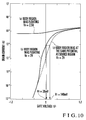
- Fig. 10 is a graph showing typical relationships between the drain current and the gate voltage in an n-channel MOS transistor formed on an SOI substrate.
- the length of the gate electrode 6 is 0.24 ⁇ m and its width is 10 ⁇ m.
- the thickness T of the body region 10 is 50 nm. This MOS transistor is so designed that the overall body region 10 is depleted when the gate voltage is OFF.
- characteristic curves (a) and (b) indicated by the solid lines were obtained when drain voltages V D , respectively, of 2 V and 2.5 V were applied while the body region 10 was in a floating state.
- a characteristic curve (c) indicated by the broken line was obtained when the source electrode 16 was also used as a dedicated electrode for the body region 10 and a drain voltage V D of 2 V was applied while the body region 10 was forcedly fixed to the source potential.
- a threshold voltage V T obtained from the characteristic curve (a) is as low as 20 mV.
- the threshold voltage V T is 140 mV on the characteristic curve (c) obtained when the body region 10 was fixed to the source potential, it is seen that the threshold voltage V T decreased by 120 mV because the body region 10 was in a floating state.
- floating the body region 10 resulted in an approximately order of magnitude higher drain current when the gate voltage was 0 V, i.e., in an OFF current.
- the characteristic curve (c) when the drain current V D was increased to 2.5 V indicates the worst state in which a large drain current kept flowing even upon application of a negative bias as the gate voltage and so the n-channel MOS transistor could not be turned off only by controlling the gate voltage.
- This state is a self-latch state which cannot be released unless the drain voltage V D is decreased.
- This problem is considered to be caused by the action of a parasitic bipolar transistor in which the n-type source region 8, p-type body region 10, and the n-type drain region 9 serve as an emitter region, a base region, and a collector region, respectively.
- a crystalline silicon substrate 1 and a source electrode 16 are grounded, and a positive drain voltage V D and a positive gate voltage V G are applied to a drain electrode 17 and a gate electrode 6, respectively.
- the electrons ( ⁇ in Fig. 11) flow into a drain region 9, and the holes (o in Fig. 11) flow into a body region 10.
- the holes flow toward a source region 8 along the bottom surface of the body region 10 with a low potential.
- a current (Ip) caused by these holes functions as the base current of a parasitic bipolar transistor.
- the holes reaching a source/body metallurgical junction 13 are injected into the source region 8 through this junction, recombine with electrons which are majority carriers in this region, and disappear.
- An electron current (In) caused by these inversely injected electrons (o in Fig. 11) is the emitter current of the parasitic bipolar transistor.
- This electron current (In) joins an inherent channel current of the MOS transistor which consists of electrons ( ⁇ in Fig. 11) induced on the upper surface of the body region 10 by the gate voltage.
- the increased electron current (In) encourages the impact ionization in the depletion layer formed in the drain/body metallurgical junction, generating a still larger number of electron-hole pairs.
- fixing the body region 10 to the source potential described earlier amounts to extracting the hole current (Ip) from the body region 10 without the intermediacy of the source/body metallurgical junction 13, and so no electron current (In) is generated in this case.
- a MOS transistor formed on an SOI substrate has excellent characteristics, i.e., can achieve a high packing density and a high operating speed.
- this MOS transistor also has problems derived from the use of the body region 10 in a floating state, i.e., problems of an increase in the OFF current and a decrease in the threshold voltage. Therefore, this MOS transistor has not been put into practical use yet.
- the present invention has been made to solve the above conventional problems and has as its object to provide a MOS transistor capable of suppressing the action of a parasitic bipolar transistor even when a body region is used in a floating state and thereby achieving both a high packing density and a high operating speed, and a method of fabricating the same.
- a minority carrier recombination region consisting of crystal defects is formed, in contact with a buried insulating film, from a position a predetermined distance from a body region, in a source region formed on the buried insulating film and made from a crystalline semiconductor.
- a rare gas element is ion-implanted to form a minority carrier recombination region consisting of crystal defects, in contact with a buried insulating film, from a position a predetermined distance from a body region, in a source region formed on the buried insulating film and made from a crystalline semiconductor.
- the ion-implanted rare gas element forms crystal defects in the crystalline semiconductor source region but does not function as carriers.
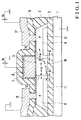
- Fig. 1 is a sectional view of an n-channel MOS transistor showing the structure of an embodiment of a MOS transistor according to the present invention.
- reference numeral 1 denotes a crystalline silicon substrate; and 2 and 3, silicon oxide films for device isolation.
- the silicon oxide film 2 is a buried insulating film on an SOI substrate.
- Reference numeral 5 denotes a gate silicon oxide film; 6, an n-type polycrystalline silicon gate electrode; and 7, a silicon oxide film for protecting the surface of the gate electrode 6.
- Reference numeral 8 denotes an n-type crystalline silicon source region formed on the silicon oxide film 2; 9, an n-type crystalline silicon drain region formed on the silicon oxide film 2; and 10, a p-type crystalline silicon body region formed between the source region 8 and the drain region 9 on the silicon oxide film 2.
- Reference numeral 11 denotes an n-type minority carrier recombination region formed in the source region 8; and 12, an n-type minority carrier recombination region formed in the drain region 9.
- Reference numeral 13 denotes a metallurgical junction between the source region 8 and the body region 10, i.e., a source/body metallurgical junction; 14, a metallurgical junction between the drain region 9 and the body region 10, i.e., a drain/body metallurgical junction; 15, a PSG film as a passivation film; 16, a source electrode; and 17, a drain electrode.
- the minority carrier recombination region 11 is a region in which crystal defects are formed, and is formed, in contact with the silicon oxide film 2, in the source region 8 from a position a distance D from the source/body metallurgical junction 13.
- the minority carrier recombination region 12 is formed, in contact with the silicon oxide film 2, in the drain region 9 from a position the distance D from the drain/body metallurgical junction 14.
- minority carrier recombination regions 11 and 12 are arranged so as not to contact a depletion layer from the body region 10. Essentially, the minority carrier recombination regions 11 and 12 are arranged so as not to contact the body region 10.
- the width of the depletion layer extending from the metallurgical junction toward the drain is very small, 0.2 nm or less, and is therefore negligible in practice.
- the thickness of the body region 10 is set to be smaller than the thickness of a depletion layer which can extend from immediately below the gate silicon oxide film 5.
- the action of a parasitic bipolar transistor can be suppressed by setting the distance D to be smaller than the diffusion length of holes in the source region 8. This will be described below.
- the crystalline substrate 1 and the source electrode 16 are grounded, and appropriate positive gate and drain voltages V G and V D are applied to the gate and drain electrodes 6 and 17, respectively.
- the holes (o in Fig. 1) flow into the body region 10.
- the holes injected into the source region 8 are forced to recombine with electrons, as majority carriers, by crystal defects in the minority carrier recombination region 11 and vanish.
- the diffusion length of holes in the source region 8 is essentially the distance D.
- In/Ip (LpE ⁇ E)/ ⁇ LnB ⁇ B ⁇ tanh(Leff/LnB) ⁇
- LpE is the diffusion length of holes in the n-type source region 8 acting as an emitter
- ⁇ E is the conductivity of the source region 8
- LnB is the diffusion length of electrons in the p-type body region 10 acting as a base
- ⁇ B is the conductivity of the body region 10
- Leff is the length of the body region 10, i.e., the effective channel length of the MOS transistor.
- the diffusion length of holes in a MOS transistor with a conventional structure not having the minority carrier recombination region 11 in the source region 8 is LpE.
- the minority carrier recombination region 11 is so arranged that the distance D is smaller than LpE, the number of electrons injected from the source region 8 into the body region 10 is decreased in accordance with the above approximation.
- the minority carrier recombination region 11 formed in the source region 8 plays an important role is suppressing a parasitic bipolar transistor. Similar effects can be obtained by the minority carrier recombination region 12 formed in the drain region 9.
- the source and drain regions 8 and 9 have the same structure and are distinguished from each other by the magnitudes of the applied voltages.
- the low-voltage side is called a source region and the high-voltage side is called a drain region.
- the minority carrier recombination region 12 must be formed in the drain region 9.
- minority carrier recombination regions are formed in an n-channel MOS transistor.
- analogous effects can be obtained in a p-channel MOS transistor by forming minority carrier recombination regions in the source and drain regions, since n- and p-channel MOS transistors are different only in the conductivity types of the source, drain, and body regions and the gate electrode.
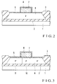
- Figs. 2 to 5 are sectional views for explaining an embodiment of a method of fabricating the n-channel MOS transistor shown in Fig. 1, in which individual fabrication steps are illustrated.
- the MOS transistor in Fig. 1 is formed on an SOI substrate on which a crystalline silicon substrate 1, a silicon oxide film 2 with a thickness of about 90 nm, and a crystalline silicon layer with a thickness of about 50 nm are stacked in this order.
- the SOI substrate used as a starting substrate can be formed by any of a deposition film recrystallization method, a crystal separation method, a heteroepitaxial deposition method, and a bonding method.
- a silicon oxide film 3 for lateral device isolation is formed by selective oxidation, thereby forming a crystalline silicon island 4 surrounded by the silicon oxide films 2 and 3.
- boron ions are implanted into the crystalline silicon island 4 to give the crystalline silicon island 4 a desired p-type impurity concentration. Subsequently, the surface of the crystalline silicon island 4 is thermally oxidized to form a gate silicon oxide film 5 about 5 nm thick.
- a phosphorus-doped polycrystalline silicon film about 300 nm thick is deposited on the gate silicon oxide film 5 by low-pressure chemical vapor deposition.
- This phosphorus-doped polycrystalline silicon film is etched into a gate electrode 6 by using a resist as a mask. After the resist is removed, the surface of the gate oxide film 6 is thermally oxidized to form a silicon oxide film 7 about 10 nm thick (Fig. 2).
- phosphorus ions are implanted by using the stacked film consisting of the gate electrode 6 and the silicon oxide film 7 as a mask and annealing is performed, thereby simultaneously forming an n-type source region 8 and an n-type drain region 9.
- a p-type crystalline silicon region sandwiched between the source region 8 and the drain region 9 is a body region 10.
- argon ions for example, are implanted with an acceleration energy of 50 keV, a does of 1 x 10 14 cm -2 , and a beam incident angle of 7° into the source region 8 and the drain region 9 by using the stacked film consisting of the gate electrode 6 and the silicon oxide film 7 as a mask.
- the projected range of argon is approximately 50 nm in the vertical direction. Accordingly, immediately after the ion implantation the position at which the concentration of argon is a maximum is near the interface between the source region 8 or the drain region 9 and the silicon oxide film 2.
- annealing is performed at 950°C for 15 sec.
- an n-type minority carrier recombination region 11 and an n-type minority carrier recombination region 12 both containing a number of crystal defects are simultaneously formed in the source region 8 and the drain region 9, respectively, at positions adjacent to the silicon oxide film 2.
- Reference symbol D in Fig. 4 denotes the distance from a source/body metallurgical junction 13 to the minority carrier recombination region 11 or the distance from a drain/body metallurgical junction 14 to the minority carrier recombination region 12.
- the distance D can be estimated to be approximately 25 nm when the following three points are taken into consideration: the source/body metallurgical junction 13 and the drain/body metallurgical junction 14 invade a distance of about 40 nm from the edge of the gate electrode 6; the thickness of the silicon oxide film 7 is about 10 nm; and the lateral standard deviation of argon is about 25 nm.
- a PSG film 15 is deposited as a passivation film, and electrode contacts are opened to form a source electrode 16 and a drain electrode 17. Finally, hydrogen annealing is performed to complete the SOI type n-channel MOS transistor illustrated in Fig. 1.
- the beam incident angle is set at 7° as the argon ion implantation condition.
- the distance D can be further decreased without adding any new fabrication step.
- the distance D can be decreased to 0 if the beam incident angle is 45°.
- the distance D can be set at a desired small value with a high controllability by a self-aligned technique which uses the argon ion implantation condition as a parameter.
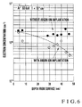
- Fig. 6 shows the distribution of the electron concentration (o in Fig. 6) in the direction of depth in the n-type source region 8 when argon ions were implanted at a dose of 1 x 10 14 cm -2 in accordance with the embodiment of the fabrication method described above.
- Fig. 6 also shows the distribution of the electron concentration ( ⁇ in Fig. 6) measured in a control sample when no argon ions were implanted.
- the electron concentration was nearly constant at approximately 2 x 10 20 cm -3 in the direction of depth.
- the electron concentration was the same as in the control sample near the surface but gradually decreased as the measurement position became deeper from the surface.
- the electron concentration was approximately 4 x 10 19 cm -3 , about 1/5 that on the surface.
- a region in which the electron concentration decreases to no more than one-half that near the surface i.e., a region containing 1 x 10 20 cm -3 or more of recombination centers is the minority carrier recombination region 11, it is evident from Fig. 6 that this recombination region is formed at a depth of 35 to 50 nm from the surface.
- a minority carrier recombination region 11 containing 1 x 10 20 cm -3 or more of recombination centers and having a thickness of about 15 nm is formed in contact with the silicon oxide film 2 at a position separated by approximately 25 nm from the source/body metallurgical junction 13.
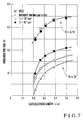
- Fig. 7 is a graph showing the results which establish, from the viewpoint of the threshold voltage, the fact that a minority carrier recombination region formed by ion implantation of argon is effective to control a parasitic bipolar transistor.
- the threshold voltage was measured by using the n-channel MOS transistor fabricated by the above embodiment. Also, in the fabrication of the transistor the dose of argon was used as a parameter.
- the threshold voltage was independent of the dose of argon.
- the threshold voltage decreased as the length of the gate electrode decreased. This is an inherent phenomenon called a short-channel effect of a MOS transistor.
- the effect of increasing the threshold voltage was enhanced when the dose was increased from 1 x 10 14 cm -2 (o in Fig. 7) to 2 x 10 14 cm -2 ( ⁇ in Fig. 7).
- Fig. 7 shows that the formation of a minority carrier recombination region is an effective means of suppressing the parasitic bipolar transistor effect.
- Japanese Patent Laid-Open No. 7-193248 has disclosed a method by which a minority carrier recombination region is formed by ion implantation of any of silicon, oxygen, carbon, and nitrogen.
- Argon used in this embodiment is superior to any of these elements for the reasons explained below.
- crystal defects when crystal defects are formed by ion implantation of silicon, these crystal defects vanish by solid-phase epitaxy if annealing is performed at a temperature higher than 600°C after the ion implantation.
- the temperature of the processing done after the ion implantation is limited to those lower than 600°C.
- Formation of crystal defects using oxygen atoms requires a special ion implantation apparatus; i.e., no versatile apparatus can readily perform oxygen ion implantation.
- the mass number of oxygen is 16 which is smaller than 40 of argon, a dose of a 10 16 cm -2 order is necessary to form crystal defects. This value is two orders of magnitude larger than a 10 14 cm -2 order required when argon is used.
- the mass number of carbon is 12, further smaller than that of oxygen. Therefore, a high dose of a 10 16 cm -2 order is required to form crystal defects, resulting in a long processing time.
- carbon ions are implanted into a gate oxide film during the ion implantation.
- the mass number of nitrogen also is small, 14, like those of oxygen and carbon, and so a high dose is required.
- nitrogen acts as a donor type impurity. Therefore, when nitrogen ions are implanted into the source region of a p-channel MOS transistor, the implanted nitrogen ions and the previously doped acceptor type impurity cancel each other out, and this may extraordinarily raise the sheet resistance of the source region.
- the channel region has a low p-type impurity concentration. Accordingly, if implanted nitrogen ions are mixed in the channel region around the source region (or the drain region), the conductivity type may change in a portion of the channel region.
- argon used in this embodiment has the characteristics explained below which none of the various elements described in Japanese Patent Laid-Open No. 7-193248 cited above has.
- argon can form crystal defects that are stable even when high-temperature annealing is performed. Since the mass number of argon is as large as 40, crystal defects can be efficiently formed with a relatively low dose.
- Argon ions can be implanted by using a general-purpose ion implantation apparatus. Argon acts as neither a donor nor acceptor type impurity.
- Japanese Patent Laid-Open No. 7-15015 has disclosed a method of controlling the action of a parasitic bipolar transistor by implanting neutral impurity ions, such as ions of krypton, xenon, germanium, or argon, into a high-field region in a drain/body metallurgical junction.
- neutral impurity ions such as ions of krypton, xenon, germanium, or argon
- the basis of this method is to decrease the mean free path of carriers by producing scattering centers in the high-field region by using the neutral impurity, thereby decreasing the number of electron-hole pairs generated by impact ionization near the drain/body metallurgical junction.
- a region into which the neutral impurity is ion-implanted is necessarily close to the drain/body metallurgical junction and also close to the surface of a body region into which a channel current flows.
- the basis of this embodiment is to form recombination centers near the source/body metallurgical junction, thereby efficiently extracting carriers accumulated in the body region into the source region. That is, the purpose of this embodiment is not to control impact ionization near the drain/body metallurgical junction.
- the implantation position is largely different from that in the conventional method, i.e., the implantation position is close to the source/body metallurgical junction and near the interface between the source region and the silicon oxide film for device isolation.
- the minority carrier recombination region 11, Fig. 1, in the source region 8, can also be formed to have an island-like planar shape on the silicon oxide film 2. This also applies to the minority carrier recombination region 12.
- Fig. 8B is more effective in which the minority carrier recombination region 11 is formed throughout the length which the gate electrode 6 extends in the source region 8. This also holds true for the minority carrier recombination region 12.
- the present invention can achieve the startling effects as presented below.
Landscapes
- Thin Film Transistor (AREA)
Applications Claiming Priority (4)
| Application Number | Priority Date | Filing Date | Title |
|---|---|---|---|
| JP75229/95 | 1995-03-31 | ||
| JP7522995 | 1995-03-31 | ||
| JP31519795 | 1995-12-04 | ||
| JP315197/95 | 1995-12-04 |
Publications (2)
| Publication Number | Publication Date |
|---|---|
| EP0735592A2 true EP0735592A2 (de) | 1996-10-02 |
| EP0735592A3 EP0735592A3 (de) | 1997-11-05 |
Family
ID=26416387
Family Applications (1)
| Application Number | Title | Priority Date | Filing Date |
|---|---|---|---|
| EP96105132A Withdrawn EP0735592A3 (de) | 1995-03-31 | 1996-03-29 | MOS-Dünnfilmtransistor und Herstellungsverfahren |
Country Status (1)
| Country | Link |
|---|---|
| EP (1) | EP0735592A3 (de) |
Cited By (3)
| Publication number | Priority date | Publication date | Assignee | Title |
|---|---|---|---|---|
| GB2358079A (en) * | 2000-01-07 | 2001-07-11 | Seiko Epson Corp | Thin film transistors |
| GB2358084A (en) * | 2000-01-07 | 2001-07-11 | Seiko Epson Corp | Field effect transistors |
| US6765265B2 (en) * | 2000-01-07 | 2004-07-20 | Seiko Epson Corporation | System and method for manufacturing a thin film transistor |
Family Cites Families (5)
| Publication number | Priority date | Publication date | Assignee | Title |
|---|---|---|---|---|
| JPS6143475A (ja) * | 1984-08-08 | 1986-03-03 | Agency Of Ind Science & Technol | Mos型半導体装置 |
| JPS6425573A (en) * | 1987-07-22 | 1989-01-27 | Hitachi Ltd | Thin film transistor |
| JP2510710B2 (ja) * | 1988-12-13 | 1996-06-26 | 三菱電機株式会社 | 絶縁体基板上の半導体層に形成されたmos型電界効果トランジスタ |
| DE69111929T2 (de) * | 1990-07-09 | 1996-03-28 | Sony Corp | Halbleiteranordnung auf einem dielektrischen isolierten Substrat. |
| EP0622834A3 (de) * | 1993-04-30 | 1998-02-11 | International Business Machines Corporation | Verfahren zur Latch-up Vermeidung und Durchbruchspannung Verbesserung in SOI MOSFET |
-
1996
- 1996-03-29 EP EP96105132A patent/EP0735592A3/de not_active Withdrawn
Cited By (6)
| Publication number | Priority date | Publication date | Assignee | Title |
|---|---|---|---|---|
| GB2358079A (en) * | 2000-01-07 | 2001-07-11 | Seiko Epson Corp | Thin film transistors |
| GB2358084A (en) * | 2000-01-07 | 2001-07-11 | Seiko Epson Corp | Field effect transistors |
| US6528830B1 (en) | 2000-01-07 | 2003-03-04 | Seiko Epson Corporation | Thin film transistor |
| GB2358084B (en) * | 2000-01-07 | 2004-02-18 | Seiko Epson Corp | Semiconductor transistor |
| GB2358079B (en) * | 2000-01-07 | 2004-02-18 | Seiko Epson Corp | Thin-film transistor |
| US6765265B2 (en) * | 2000-01-07 | 2004-07-20 | Seiko Epson Corporation | System and method for manufacturing a thin film transistor |
Also Published As
| Publication number | Publication date |
|---|---|
| EP0735592A3 (de) | 1997-11-05 |
Similar Documents
| Publication | Publication Date | Title |
|---|---|---|
| US7064399B2 (en) | Advanced CMOS using super steep retrograde wells | |
| US4965213A (en) | Silicon-on-insulator transistor with body node to source node connection | |
| US4946799A (en) | Process for making high performance silicon-on-insulator transistor with body node to source node connection | |
| US5212397A (en) | BiCMOS device having an SOI substrate and process for making the same | |
| US5041885A (en) | Surface field effect transistor with depressed source and/or drain areas for ULSI integrated devices | |
| US5527724A (en) | Method to prevent latch-up and improve breakdown volatge in SOI mosfets | |
| EP0458570B1 (de) | Diode und Halbleiterbauelement mit einer Diode | |
| US4680603A (en) | Graded extended drain concept for reduced hot electron effect | |
| EP0208935A1 (de) | FET mit schmalem Kanal | |
| US6358783B1 (en) | Semiconductor device and method of manufacturing the same | |
| US4922315A (en) | Control gate lateral silicon-on-insulator bipolar transistor | |
| US5726459A (en) | GE-SI SOI MOS transistor and method of fabricating same | |
| WO1996029733A1 (en) | Self-aligned edge control in silicon on insulator | |
| WO1993019482A1 (en) | Threshold adjustment in vertical dmos devices | |
| US6437406B1 (en) | Super-halo formation in FETs | |
| EP0772241B1 (de) | Leistungsbauteil hoher Dichte in MOS-Technologie | |
| KR910000279B1 (ko) | 금속 산화물 반도체 전계효과 트랜지스터 및 이 트랜지스터의 소스 및 드레인 영역 형성방법 | |
| JP3103159B2 (ja) | 半導体装置 | |
| US7485923B2 (en) | SOI semiconductor device with improved halo region and manufacturing method of the same | |
| US3814992A (en) | High performance fet | |
| US5242849A (en) | Method for the fabrication of MOS devices | |
| US6528846B1 (en) | Asymmetric high voltage silicon on insulator device design for input output circuits | |
| US5731637A (en) | Semiconductor device | |
| US6452233B1 (en) | SOI device having a leakage stopping layer | |
| EP0735592A2 (de) | MOS-Dünnfilmtransistor und Herstellungsverfahren |
Legal Events
| Date | Code | Title | Description |
|---|---|---|---|
| PUAI | Public reference made under article 153(3) epc to a published international application that has entered the european phase |
Free format text: ORIGINAL CODE: 0009012 |
|
| AK | Designated contracting states |
Kind code of ref document: A2 Designated state(s): DE FR GB |
|
| PUAL | Search report despatched |
Free format text: ORIGINAL CODE: 0009013 |
|
| AK | Designated contracting states |
Kind code of ref document: A3 Designated state(s): DE FR GB |
|
| STAA | Information on the status of an ep patent application or granted ep patent |
Free format text: STATUS: THE APPLICATION IS DEEMED TO BE WITHDRAWN |
|
| 18D | Application deemed to be withdrawn |
Effective date: 19980504 |