EP0734072A2 - Insulated gate semiconductor device and method of manufacture - Google Patents
Insulated gate semiconductor device and method of manufacture Download PDFInfo
- Publication number
- EP0734072A2 EP0734072A2 EP96103289A EP96103289A EP0734072A2 EP 0734072 A2 EP0734072 A2 EP 0734072A2 EP 96103289 A EP96103289 A EP 96103289A EP 96103289 A EP96103289 A EP 96103289A EP 0734072 A2 EP0734072 A2 EP 0734072A2
- Authority
- EP
- European Patent Office
- Prior art keywords
- gate structure
- layer
- gate
- dopant
- dielectric material
- Prior art date
- Legal status (The legal status is an assumption and is not a legal conclusion. Google has not performed a legal analysis and makes no representation as to the accuracy of the status listed.)
- Withdrawn
Links
- 239000004065 semiconductor Substances 0.000 title claims abstract description 50
- 238000000034 method Methods 0.000 title claims description 27
- 238000004519 manufacturing process Methods 0.000 title abstract description 9
- 239000002019 doping agent Substances 0.000 claims abstract description 106
- 239000000463 material Substances 0.000 claims description 54
- 239000003989 dielectric material Substances 0.000 claims description 45
- 229910021420 polycrystalline silicon Inorganic materials 0.000 claims description 33
- 229920005591 polysilicon Polymers 0.000 claims description 33
- 239000012535 impurity Substances 0.000 claims description 32
- 125000006850 spacer group Chemical group 0.000 claims description 32
- 239000004020 conductor Substances 0.000 claims description 29
- 238000005530 etching Methods 0.000 claims description 7
- 229910021417 amorphous silicon Inorganic materials 0.000 claims description 3
- 229910021421 monocrystalline silicon Inorganic materials 0.000 claims description 3
- WFKWXMTUELFFGS-UHFFFAOYSA-N tungsten Chemical compound [W] WFKWXMTUELFFGS-UHFFFAOYSA-N 0.000 claims description 3
- 229910052721 tungsten Inorganic materials 0.000 claims description 3
- 239000010937 tungsten Substances 0.000 claims description 3
- 238000000151 deposition Methods 0.000 claims description 2
- 230000005669 field effect Effects 0.000 abstract description 31
- 239000000758 substrate Substances 0.000 abstract description 6
- 239000007943 implant Substances 0.000 description 73
- 229920002120 photoresistant polymer Polymers 0.000 description 40
- 229910021332 silicide Inorganic materials 0.000 description 32
- FVBUAEGBCNSCDD-UHFFFAOYSA-N silicide(4-) Chemical compound [Si-4] FVBUAEGBCNSCDD-UHFFFAOYSA-N 0.000 description 32
- 229910052581 Si3N4 Inorganic materials 0.000 description 18
- HQVNEWCFYHHQES-UHFFFAOYSA-N silicon nitride Chemical compound N12[Si]34N5[Si]62N3[Si]51N64 HQVNEWCFYHHQES-UHFFFAOYSA-N 0.000 description 18
- ZOXJGFHDIHLPTG-UHFFFAOYSA-N Boron Chemical compound [B] ZOXJGFHDIHLPTG-UHFFFAOYSA-N 0.000 description 17
- 229910052796 boron Inorganic materials 0.000 description 17
- 230000015572 biosynthetic process Effects 0.000 description 16
- 230000000295 complement effect Effects 0.000 description 8
- OAICVXFJPJFONN-UHFFFAOYSA-N Phosphorus Chemical compound [P] OAICVXFJPJFONN-UHFFFAOYSA-N 0.000 description 6
- 229910052698 phosphorus Inorganic materials 0.000 description 6
- 239000011574 phosphorus Substances 0.000 description 6
- BOTDANWDWHJENH-UHFFFAOYSA-N Tetraethyl orthosilicate Chemical group CCO[Si](OCC)(OCC)OCC BOTDANWDWHJENH-UHFFFAOYSA-N 0.000 description 5
- 230000007423 decrease Effects 0.000 description 4
- 230000004048 modification Effects 0.000 description 4
- 238000012986 modification Methods 0.000 description 4
- 238000007254 oxidation reaction Methods 0.000 description 4
- 230000003647 oxidation Effects 0.000 description 3
- KRHYYFGTRYWZRS-UHFFFAOYSA-N Fluorane Chemical compound F KRHYYFGTRYWZRS-UHFFFAOYSA-N 0.000 description 2
- 229910052785 arsenic Inorganic materials 0.000 description 2
- RQNWIZPPADIBDY-UHFFFAOYSA-N arsenic atom Chemical compound [As] RQNWIZPPADIBDY-UHFFFAOYSA-N 0.000 description 2
- 239000011248 coating agent Substances 0.000 description 2
- 238000000576 coating method Methods 0.000 description 2
- 230000008878 coupling Effects 0.000 description 2
- 238000010168 coupling process Methods 0.000 description 2
- 238000005859 coupling reaction Methods 0.000 description 2
- 238000000354 decomposition reaction Methods 0.000 description 2
- 238000004518 low pressure chemical vapour deposition Methods 0.000 description 2
- 230000001590 oxidative effect Effects 0.000 description 2
- 238000005229 chemical vapour deposition Methods 0.000 description 1
- 230000008021 deposition Effects 0.000 description 1
- 230000000694 effects Effects 0.000 description 1
- 150000002500 ions Chemical class 0.000 description 1
- 150000004767 nitrides Chemical class 0.000 description 1
Images


Classifications
-
- H—ELECTRICITY
- H01—ELECTRIC ELEMENTS
- H01L—SEMICONDUCTOR DEVICES NOT COVERED BY CLASS H10
- H01L29/00—Semiconductor devices adapted for rectifying, amplifying, oscillating or switching, or capacitors or resistors with at least one potential-jump barrier or surface barrier, e.g. PN junction depletion layer or carrier concentration layer; Details of semiconductor bodies or of electrodes thereof ; Multistep manufacturing processes therefor
- H01L29/40—Electrodes ; Multistep manufacturing processes therefor
- H01L29/43—Electrodes ; Multistep manufacturing processes therefor characterised by the materials of which they are formed
- H01L29/49—Metal-insulator-semiconductor electrodes, e.g. gates of MOSFET
- H01L29/4983—Metal-insulator-semiconductor electrodes, e.g. gates of MOSFET with a lateral structure, e.g. a Polysilicon gate with a lateral doping variation or with a lateral composition variation or characterised by the sidewalls being composed of conductive, resistive or dielectric material
-
- H—ELECTRICITY
- H01—ELECTRIC ELEMENTS
- H01L—SEMICONDUCTOR DEVICES NOT COVERED BY CLASS H10
- H01L29/00—Semiconductor devices adapted for rectifying, amplifying, oscillating or switching, or capacitors or resistors with at least one potential-jump barrier or surface barrier, e.g. PN junction depletion layer or carrier concentration layer; Details of semiconductor bodies or of electrodes thereof ; Multistep manufacturing processes therefor
- H01L29/66—Types of semiconductor device ; Multistep manufacturing processes therefor
- H01L29/68—Types of semiconductor device ; Multistep manufacturing processes therefor controllable by only the electric current supplied, or only the electric potential applied, to an electrode which does not carry the current to be rectified, amplified or switched
- H01L29/70—Bipolar devices
- H01L29/72—Transistor-type devices, i.e. able to continuously respond to applied control signals
- H01L29/739—Transistor-type devices, i.e. able to continuously respond to applied control signals controlled by field-effect, e.g. bipolar static induction transistors [BSIT]
-
- H—ELECTRICITY
- H01—ELECTRIC ELEMENTS
- H01L—SEMICONDUCTOR DEVICES NOT COVERED BY CLASS H10
- H01L21/00—Processes or apparatus adapted for the manufacture or treatment of semiconductor or solid state devices or of parts thereof
- H01L21/70—Manufacture or treatment of devices consisting of a plurality of solid state components formed in or on a common substrate or of parts thereof; Manufacture of integrated circuit devices or of parts thereof
- H01L21/77—Manufacture or treatment of devices consisting of a plurality of solid state components or integrated circuits formed in, or on, a common substrate
- H01L21/78—Manufacture or treatment of devices consisting of a plurality of solid state components or integrated circuits formed in, or on, a common substrate with subsequent division of the substrate into plural individual devices
- H01L21/82—Manufacture or treatment of devices consisting of a plurality of solid state components or integrated circuits formed in, or on, a common substrate with subsequent division of the substrate into plural individual devices to produce devices, e.g. integrated circuits, each consisting of a plurality of components
- H01L21/822—Manufacture or treatment of devices consisting of a plurality of solid state components or integrated circuits formed in, or on, a common substrate with subsequent division of the substrate into plural individual devices to produce devices, e.g. integrated circuits, each consisting of a plurality of components the substrate being a semiconductor, using silicon technology
- H01L21/8232—Field-effect technology
- H01L21/8234—MIS technology, i.e. integration processes of field effect transistors of the conductor-insulator-semiconductor type
- H01L21/8238—Complementary field-effect transistors, e.g. CMOS
- H01L21/823857—Complementary field-effect transistors, e.g. CMOS with a particular manufacturing method of the gate insulating layers, e.g. different gate insulating layer thicknesses, particular gate insulator materials or particular gate insulator implants
-
- H—ELECTRICITY
- H01—ELECTRIC ELEMENTS
- H01L—SEMICONDUCTOR DEVICES NOT COVERED BY CLASS H10
- H01L29/00—Semiconductor devices adapted for rectifying, amplifying, oscillating or switching, or capacitors or resistors with at least one potential-jump barrier or surface barrier, e.g. PN junction depletion layer or carrier concentration layer; Details of semiconductor bodies or of electrodes thereof ; Multistep manufacturing processes therefor
- H01L29/02—Semiconductor bodies ; Multistep manufacturing processes therefor
- H01L29/06—Semiconductor bodies ; Multistep manufacturing processes therefor characterised by their shape; characterised by the shapes, relative sizes, or dispositions of the semiconductor regions ; characterised by the concentration or distribution of impurities within semiconductor regions
- H01L29/10—Semiconductor bodies ; Multistep manufacturing processes therefor characterised by their shape; characterised by the shapes, relative sizes, or dispositions of the semiconductor regions ; characterised by the concentration or distribution of impurities within semiconductor regions with semiconductor regions connected to an electrode not carrying current to be rectified, amplified or switched and such electrode being part of a semiconductor device which comprises three or more electrodes
- H01L29/107—Substrate region of field-effect devices
- H01L29/1075—Substrate region of field-effect devices of field-effect transistors
- H01L29/1079—Substrate region of field-effect devices of field-effect transistors with insulated gate
- H01L29/1083—Substrate region of field-effect devices of field-effect transistors with insulated gate with an inactive supplementary region, e.g. for preventing punch-through, improving capacity effect or leakage current
-
- H—ELECTRICITY
- H01—ELECTRIC ELEMENTS
- H01L—SEMICONDUCTOR DEVICES NOT COVERED BY CLASS H10
- H01L29/00—Semiconductor devices adapted for rectifying, amplifying, oscillating or switching, or capacitors or resistors with at least one potential-jump barrier or surface barrier, e.g. PN junction depletion layer or carrier concentration layer; Details of semiconductor bodies or of electrodes thereof ; Multistep manufacturing processes therefor
- H01L29/40—Electrodes ; Multistep manufacturing processes therefor
- H01L29/41—Electrodes ; Multistep manufacturing processes therefor characterised by their shape, relative sizes or dispositions
- H01L29/423—Electrodes ; Multistep manufacturing processes therefor characterised by their shape, relative sizes or dispositions not carrying the current to be rectified, amplified or switched
- H01L29/42312—Gate electrodes for field effect devices
- H01L29/42316—Gate electrodes for field effect devices for field-effect transistors
- H01L29/4232—Gate electrodes for field effect devices for field-effect transistors with insulated gate
- H01L29/42372—Gate electrodes for field effect devices for field-effect transistors with insulated gate characterised by the conducting layer, e.g. the length, the sectional shape or the lay-out
- H01L29/42376—Gate electrodes for field effect devices for field-effect transistors with insulated gate characterised by the conducting layer, e.g. the length, the sectional shape or the lay-out characterised by the length or the sectional shape
-
- H—ELECTRICITY
- H01—ELECTRIC ELEMENTS
- H01L—SEMICONDUCTOR DEVICES NOT COVERED BY CLASS H10
- H01L29/00—Semiconductor devices adapted for rectifying, amplifying, oscillating or switching, or capacitors or resistors with at least one potential-jump barrier or surface barrier, e.g. PN junction depletion layer or carrier concentration layer; Details of semiconductor bodies or of electrodes thereof ; Multistep manufacturing processes therefor
- H01L29/40—Electrodes ; Multistep manufacturing processes therefor
- H01L29/43—Electrodes ; Multistep manufacturing processes therefor characterised by the materials of which they are formed
- H01L29/49—Metal-insulator-semiconductor electrodes, e.g. gates of MOSFET
- H01L29/4983—Metal-insulator-semiconductor electrodes, e.g. gates of MOSFET with a lateral structure, e.g. a Polysilicon gate with a lateral doping variation or with a lateral composition variation or characterised by the sidewalls being composed of conductive, resistive or dielectric material
- H01L29/4991—Metal-insulator-semiconductor electrodes, e.g. gates of MOSFET with a lateral structure, e.g. a Polysilicon gate with a lateral doping variation or with a lateral composition variation or characterised by the sidewalls being composed of conductive, resistive or dielectric material comprising an air gap
-
- H—ELECTRICITY
- H01—ELECTRIC ELEMENTS
- H01L—SEMICONDUCTOR DEVICES NOT COVERED BY CLASS H10
- H01L29/00—Semiconductor devices adapted for rectifying, amplifying, oscillating or switching, or capacitors or resistors with at least one potential-jump barrier or surface barrier, e.g. PN junction depletion layer or carrier concentration layer; Details of semiconductor bodies or of electrodes thereof ; Multistep manufacturing processes therefor
- H01L29/66—Types of semiconductor device ; Multistep manufacturing processes therefor
- H01L29/66007—Multistep manufacturing processes
- H01L29/66075—Multistep manufacturing processes of devices having semiconductor bodies comprising group 14 or group 13/15 materials
- H01L29/66227—Multistep manufacturing processes of devices having semiconductor bodies comprising group 14 or group 13/15 materials the devices being controllable only by the electric current supplied or the electric potential applied, to an electrode which does not carry the current to be rectified, amplified or switched, e.g. three-terminal devices
- H01L29/66409—Unipolar field-effect transistors
- H01L29/66477—Unipolar field-effect transistors with an insulated gate, i.e. MISFET
- H01L29/66568—Lateral single gate silicon transistors
- H01L29/66659—Lateral single gate silicon transistors with asymmetry in the channel direction, e.g. lateral high-voltage MISFETs with drain offset region, extended drain MISFETs
-
- H—ELECTRICITY
- H01—ELECTRIC ELEMENTS
- H01L—SEMICONDUCTOR DEVICES NOT COVERED BY CLASS H10
- H01L29/00—Semiconductor devices adapted for rectifying, amplifying, oscillating or switching, or capacitors or resistors with at least one potential-jump barrier or surface barrier, e.g. PN junction depletion layer or carrier concentration layer; Details of semiconductor bodies or of electrodes thereof ; Multistep manufacturing processes therefor
- H01L29/66—Types of semiconductor device ; Multistep manufacturing processes therefor
- H01L29/68—Types of semiconductor device ; Multistep manufacturing processes therefor controllable by only the electric current supplied, or only the electric potential applied, to an electrode which does not carry the current to be rectified, amplified or switched
- H01L29/76—Unipolar devices, e.g. field effect transistors
- H01L29/772—Field effect transistors
- H01L29/78—Field effect transistors with field effect produced by an insulated gate
- H01L29/7833—Field effect transistors with field effect produced by an insulated gate with lightly doped drain or source extension, e.g. LDD MOSFET's; DDD MOSFET's
- H01L29/7835—Field effect transistors with field effect produced by an insulated gate with lightly doped drain or source extension, e.g. LDD MOSFET's; DDD MOSFET's with asymmetrical source and drain regions, e.g. lateral high-voltage MISFETs with drain offset region, extended drain MISFETs
Definitions
- the present invention relates, in general, to insulated gate semiconductor devices, and more particularly, to controlling a threshold voltage, V T , and increasing a transconductance, g m , of insulated gate semiconductor devices.
- V T is related to the voltage at which an insulated gate semiconductor device turns on and varies in accordance with the carrier concentration of the channel region.
- V GS gate-source voltage
- the gate-source voltage (V GS ) of an N-channel insulated gate semiconductor device must exceed V T to form a channel in the insulated gate semiconductor device.
- the voltage at the gate is typically the input voltage of the insulated gate semiconductor device, the input voltage relative to the source voltage must exceed V T for a conducting channel to be formed.
- I D drain current
- V T is important in determining the saturation current of an insulated gate semiconductor device, which in turn helps determine the power bandwidth of the device.
- V T Although precise control of V T is highly desirable in all insulated gate semiconductor device applications, it is particularly important in low voltage applications.
- the difference between the upper power supply rail (5 volts) and the lower power supply rail (0 volts) is sufficiently large, i.e., approximately 5 volts, that fluctuations in V T have a negligible effect on the device performance.
- V T represents a substantial portion of the total power supply voltage. Consequently, fluctuations in V T result in large fluctuations of the current drive capability of the insulated gate semiconductor device.
- the transconductance, g m of the insulated gate field effect transistors is influenced by their V GS , I D , and V T . Since the transconductance increases as I D increases, it is desirable to maximize I D , thereby increasing the transconductance. Further, a high frequency switching speed of the insulated gate field effect transistors is reduced by the combination of the gate to drain capacitance and the gate to source capacitances, collectively referred to as gate capacitances. Thus, a large gate capacitance lowers decreases the bandwidth or lowers the frequency response of the insulated gate field effect transistor.
- an insulated gate field effect transistor and method of manufacturing the insulated gate field effect transistor that provides control of the threshold voltage and minimization of the gate capacitance in low voltage, high bandwidth applications.
- the present invention provides an insulated gate semiconductor device and a method of fabricating or forming the insulated gate semiconductor device.
- Insulated gate semiconductor devices are also referred to as insulated gate field effect devices and insulated gate field effect transistors.
- the insulated gate semiconductor devices manufactured in accordance with the present invention have a reduced gate capacitance, thus a higher frequency response or bandwidth, compared to insulated gate semiconductor devices manufactured by other methods.
- the insulated gate semiconductor devices of the present invention have a lightly doped drain (LDD) extension at a drain region of the device which permits formation of a thicker gate dielectric material between the portion of the gate structure adjacent the drain region and the lightly doped drain extension region.
- LDD lightly doped drain
- the gate structure comprises two conductive portions: a conductive portion near the drain region of the device which serves as a shunt electrode and an extension, i.e., a second conductive portion, adjacent the source region of the device which serves as an active gate structure.
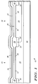
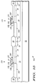
- FIG. 1 illustrates an enlarged cross-sectional view of a portion of partially completed complementary insulated gate field effect transistors 10 during processing in accordance with a first embodiment of the present invention.
- Complementary insulated gate field effect transistors 10 include an N-channel transistor 15 fabricated in a portion of a P-type epitaxial layer 13 and a P-channel transistor 16 fabricated in a portion of an N-well 14.
- a substrate 11 of P conductivity type having an epitaxial layer 13 disposed thereon.
- epitaxial layer 13 is of P conductivity type, has a major surface 12, and ranges in thickness between approximately 2 microns ( ⁇ m) and 5 ⁇ m.
- an impurity well 14 of N conductivity type is formed in a portion of P-type epitaxial layer 13.
- Substrate 11 has, for example, a resistivity ranging from approximately 0.01 ohm-centimeter ( ⁇ -cm) to approximately 0.1 ⁇ -cm, and P-type epitaxial layer 13 has a resistivity between approximately 6 ⁇ -cm and approximately 8 ⁇ -cm.
- P-type epitaxial layer 13 and N-well 14 have a surface concentration on the order of 5 X 10 15 atoms per cubic centimeter (atoms/cm 3 ).
- insulated gate field effect transistors of the present invention may be manufactured in a semiconductor material such as substrate 11.
- field implant regions 22 are formed in P-type epitaxial layer 13
- field implant regions 23 are formed in N-well 14
- field oxide regions 24 are formed over field implant regions 22 and 23. Formation of epitaxial layers, dopant wells, field implant regions, and field oxide regions are well known to those skilled in the art.
- An implant block mask (not shown) such as, for example, photoresist, is formed over N-well 14 and an impurity material of N conductivity type is implanted into a portion of P-type epitaxial layer 13 to form a dopant layer 25 between two adjacent field oxide regions 24.
- dopant layer 25 is shown as extending across an entire portion of P-type epitaxial layer 13 between adjacent field oxide regions 24, it should be understood that dopant layer 25 may be formed to extend across a subportion of the P-type epitaxial layer 13 that is between adjacent field oxide regions 24.
- the implant block mask is removed and an implant block mask is formed on the P-type epitaxial layer 13.
- An impurity material of P conductivity type is implanted into a portion of N-well 14 to form a dopant layer 30 between two adjacent field oxide regions 24. Similar to dopant layer 25, dopant layer 30 may be formed to extend across a subportion of N-well 14. It should be noted that dopant layers 25 and 30 serve as drain extension regions for field effect transistors manufactured in P-type epitaxial layer 13 and N-well 14, respectively. Further, dopant layers 25 and 30 permit the formation of a portion of the gate oxide layer to be sufficiently thick to reduce the gate capacitance, thereby improving the frequency response of the field effect transistors.
- layers 25 and 30 have a surface concentration ranging from approximately 7 x 10 16 atoms/cm 3 to approximately 2 x 10 17 atoms/cm 3 .
- a suitable set of implant conditions to obtain the aforementioned surface concentration includes: an implant dose ranging from approximately 1 x 10 12 atoms per square centimeter (atoms/cm 2 ) to approximately 3 x 10 12 atoms/cm 2 for both layers 25 and 30; an implant energy for forming dopant layer 25 ranging from approximately 50 kilo-electron volts (KeV) to approximately 200 KeV; and an implant energy for forming dopant layer 30 ranging from approximately 25 KeV to approximately 100 KeV.
- KeV kilo-electron volts
- a layer of dielectric material 26 is formed on major surface 12. Although some oxidation procedures increase the thickness of field oxide regions 24 during the formation of oxide layer 26, to simplify the description of the present invention and because the increase in thickness is small relative to the overall thickness of field oxide regions 24, the increase in the thickness of field oxide region 24 is not shown.
- a suitable technique for forming oxide layer 26 is thermal oxidation.
- oxide layer 26 has a thickness of at least 400 angstroms.
- oxide layer 26 has a thickness in the range of approximately 600 angstroms to approximately 1,800 angstroms.
- a typical thickness of oxide layer 26 is approximately 1,200 angstroms. It should be noted that portions of oxide layer 26 serve as portions of a gate oxide for transistors 15 and 16.
- a layer of polysilicon 27 is formed on oxide layer 26 using, for example, a chemical vapor deposition technique.
- a suitable thickness range for polysilicon layer 27 is from approximately 2,500 angstroms to approximately 4,000 angstroms.
- a typical thickness for polysilicon layer 27 is approximately 3,300 angstroms.
- a layer of dielectric material 28 is formed on polysilicon layer 27.
- layer of dielectric material 28 is a layer of oxide formed by the decomposition of tetraethyl orthosilicate (TEOS). Oxide layers formed by the decomposition of tetraethyl orthosilicate are commonly referred to as TEOS layers.
- TEOS tetraethyl orthosilicate
- oxide layer 28 has a thickness ranging from approximately 50 angstroms to approximately 400 angstroms and a nominal thickness of approximately 150 angstroms.
- a layer of silicon nitride 29 is formed on layer of dielectric material 28 using, for example, a low pressure chemical vapor deposition (LPCVD) technique.
- LPCVD low pressure chemical vapor deposition
- a suitable range of thicknesses for silicon nitride layer 29 is between approximately 150 angstroms and approximately 350 angstroms, and nominal thickness for silicon nitride layer 29 is approximately 250 angstroms.
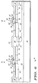
- portions 32 and 33 of the gate structures are formed over a portion of P-type epitaxial layer 13 and over a portion of N-well 14.
- Gate shunt portions 32 and 33 form part of gate structures 61 and 62, respectively, and are shown and further described in FIG. 8. It should be noted that portions 32 and 33 are formed from polysilicon layer 27 and that portion 32 has sides 36 and 37, and a top surface 45, and portion 33 has sides 38 and 39, and a top surface 50.
- Portions 32 and 33 serve as gate shunt portions of gate structures and are formed by anisotropically etching nitride layer 29, oxide layer 28, and polysilicon layer 27.
- Gate shunt portions 32 and 33 may be formed, for example, by coating silicon nitride layer 29 with a layer of photoresist (not shown), exposing the portions of silicon nitride layer 29 to be removed (using, for example, photolithographic techniques), and anisotropically etching the exposed portions of silicon nitride layer 29.
- the portions of oxide layer 28 and polysilicon layer 27 below the exposed portions of silicon nitride layer 29 are also etched, thereby exposing portions of oxide layer 26 and field oxide regions 24.
- oxide layer 41 is formed on exposed sides 36, 37, 38, and 39 of the respective gate shunt portions 32 and 33.
- oxide layer 41 is formed by thermally oxidizing the sides 36, 37, 38, and 39.
- a suitable thickness range for oxide layer 41 is between approximately 50 angstroms and approximately 250 angstroms, and a nominal thickness of oxide layer 41 is approximately 100 angstroms.
- a conformal layer of dielectric material 43 is formed on gate shunt portions 32 and 33 as well as on oxide layer 26 and field oxide regions 24.
- layer of dielectric material 43 is silicon nitride having a thickness ranging from approximately 250 angstroms to approximately 750 angstroms, and a nominal thickness of approximately 400 angstroms. It should be noted that the impurity materials of dopant layers 25 and 30 are activated or driven into P-type epitaxial layer 13 and N-well 14, respectively, by the processing steps described supra.
- silicon nitride layer 43 is anisotropically etched to form spacers 46, 46', 47, and 47' adjacent oxide layer 41.
- a suitable technique for etching silicon nitride layer 43 includes a reactive ion etch (RIE) using etchants such as CF 4 , NF 3 , and the like.
- the anisotropic etch step may remove a portion of oxide layer 26.
- oxide layer 26 is thinned to approximately 400 angstroms after the formation of spacers 46, 46', 47, and 47'. It should be noted that spacers 46 and 47 protect portions of oxide layer 26 and that spacers 46' and 47' shape oxide layer 26 in order to create a repeatable undercut etch profile (shown in FIG. 5).
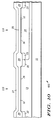
- a layer of photoresist (not shown) is formed on subportions of gate shunt portions 32 and 33 and on spacers 46 and 47.
- Spacers 46' and 47' and the portions of oxide layers 26 and 28 which are not covered by the layer of photoresist are removed via a sequence of isotropic etches, i.e., a first etch step to remove spacers 46' and 47' and a second etch step to remove portions of oxide layer 26 between gate shunt portion 32 and a first portion of major surface 12 as well as the portion of oxide layer 26 between gate shunt portion 33 and a second portion of major surface 12.
- gate shunt portions 32 and 33 are undercut on one side to form a cavity 35 underneath gate shunt portion 32, i.e., between gate shunt portion 32 and the first portion of major surface 12 and a cavity 35' underneath gate shunt portion 33, i.e., between gate shunt portion 33 and the second portion of major surface 12.
- the layer of photoresist is removed.
- a screen oxide 40 is formed on the exposed portions of gate shunt portions 32 and 33, respectively, and on the exposed portions of major surface 12.
- oxide layer 40 has a thickness ranging from approximately 100 angstroms to approximately 200 angstroms, with a nominal thickness of approximately 150 angstroms.
- oxide layer 40 is also formed on field oxide regions 24 and oxide layer 26, it should be noted that to simplify the description of the present invention, these portions of oxide layer 40 are not shown.
- a layer of photoresist (not shown) is formed on portions of oxide 40 disposed on gate shunt portions 32 and 33, spacers 46 and 47, portions of oxide layer 40 adjacent sides 37 and 39, and portions of field oxide regions 24. This layer of photoresist serves as an implant block mask.
- An enhanced dopant region 51 is formed by doping a portion of P-type epitaxial layer 13 with an impurity material of P conductivity type such as, for example, boron. More particularly, the boron is implanted into a portion of P-type epitaxial layer 13 to form dopant region 51. Dopant region 51 is laterally aligned to field oxide region 24 of N-channel transistor 15 and oxide layer 40 disposed on side 36 of gate shunt portion 32. It should be noted that dopant region 51 is spaced apart from major surface 12.
- an impurity material of P conductivity type such as, for example, boron. More particularly, the boron is implanted into a portion of P-type epitaxial layer 13 to form dopant region 51.
- Dopant region 51 is laterally aligned to field oxide region 24 of N-channel transistor 15 and oxide layer 40 disposed on side 36 of gate shunt portion 32. It should be noted that dopant region 51 is spaced apart from major surface 12.
- a suitable set of implant parameters includes implanting the P type impurity material at a dose ranging from approximately 2 x 10 12 atoms/cm 2 to approximately 2 x 10 13 atoms/cm 2 at an implant energy ranging from approximately 40 KeV to approximately 100 KeV.
- the boron that forms dopant region 51 is implanted into P-type epitaxial layer 13 to a depth or distance ranging between approximately 1,500 and approximately 3,000 angstroms.
- the impurity materials or dopant forming dopant region 51 serves to provide punch-through protection for N-channel transistor 15.
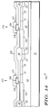
- An enhanced dopant region 52 is formed by doping another portion of P-type epitaxial layer 13 with boron.
- implant parameters for the formation of dopant region 52 include a dose ranging from approximately 5 x 10 11 atoms/cm 2 to approximately 1 x 10 13 atoms/cm 2 and a suitable implant energy ranging from approximately 10 KeV to approximately 20 KeV.
- the boron that forms dopant region 52 is implanted into a portion of P-type epitaxial layer 13 to a depth or distance ranging from approximately 200 to approximately 1,200 angstroms.
- the impurity materials forming dopant region 52 serves to adjust the threshold voltage of N-channel transistor 15.
- the layer of photoresist is removed and a layer of photoresist (not shown) is formed on portions of screen oxide 40 disposed on gate shunt portions 32 and 33, spacer 47, portions of oxide layer 26 adjacent spacer 47, portions of oxide layer 26 over P-type epitaxial layer 13, and portions of field oxide regions 24.
- This layer of photoresist also serves as an implant block mask.
- An enhanced dopant region 53 is formed by doping a portion of N-well 14 with an impurity material of N conductivity type such as, for example, phosphorus. More particularly, the phosphorus is implanted into N-well 14 to form dopant region 53. It should be noted that dopant region 53 is spaced apart from surface 12.
- a suitable set of implant parameters includes implanting the N type impurity material at a dose ranging from approximately 2 x 10 12 atoms/cm 2 to approximately 2 x 10 13 atoms/cm 2 at an implant energy ranging from approximately 80 KeV to approximately 200 KeV.
- the N type impurity material of the implant step that forms dopant region 53 is implanted into N-well 14 to a depth or distance ranging from approximately 1,500 to approximately 3,000 angstroms.
- the impurity materials forming dopant region 53 serves to provide punch-through protection for P-channel transistor 16.
- An enhanced dopant region 54 is formed by doping another portion of N-well 14 with phosphorus.
- the boron is implanted into N-well 14 to form dopant region 54.
- Suitable implant parameters for the formation of dopant region 54 include a dose ranging from approximately 5 x 10 11 atoms/cm 2 to approximately 1 x 10 13 atoms/cm 2 and a suitable implant energy ranging from approximately 20 KeV to approximately 40 KeV.
- the N type impurity material of the implant step that forms dopant region 54 is implanted into N-well 14 to a depth or distance ranging from approximately 200 to 1,200 angstroms.
- the impurity materials forming dopant region 54 serves to adjust the threshold voltage of P-channel transistor 16.
- the layer of photoresist is removed.
- screen oxide 40 is removed from gate shunt portions 32 and 33, respectively, and portions of major surface 12, thereby exposing subportions of gate shunt portions 32 and 33 and portions of major surface 12 and forming oxide extensions 55.
- An oxide layer 26' is formed on the exposed portions of major surface 12 and the exposed regions of gate shunt portions 32 and 33.
- a conformal layer of polysilicon 57 having a thickness ranging between approximately 1,000 angstroms and approximately 2,500 angstroms is deposited on oxide layers 24, 26', 41, and on spacers 46 and 47. Nominally, polysilicon layer 57 has a thickness of approximately 1,750 angstroms.
- dopant regions 51 and 52 are initially spaced apart, it should be noted that they diffuse towards each other and form a single dopant region 51'.
- dopant regions 53 and 54 diffuse towards each other and form a single dopant region 53'.
- polysilicon layer 57 is anisotropically etched to form gate extensions 58 and 59 adjacent sides 36 and 38, respectively. It should be noted that gate extensions 58 and 59 are spaced apart from the respective sides 36 and 38 by portions of oxide layer 26'. In addition, extensions 58' and 59' are formed adjacent spacers 46 and 47, respectively.
- the anisotropic etch step that forms gate extensions 58, 58', 59, and 59' stops on or in oxide layer 26'.
- gate structure 61 comprises a gate shunt portion 32 formed from a first polysilicon portion on the oxide layer 26 of a first width and a gate extension portion 58 formed from a second polysilicon portion on a portion of oxide layer 26' of a second width, wherein the second width is less than the first width.
- gate structure 62 comprises a gate shunt portion 33 formed from a polysilicon portion on the oxide layer 26 of the first width and a gate extension portion 59 formed from a another polysilicon portion on a portion of oxide layer 26' of the second width.
- a layer of photoresist (not shown) is formed on gate shunt portions 32 and 33, gate extensions 58 and 59, and the portions of oxide layer 26' adjacent gate extensions 58 and 59.
- gate extensions 58' and 59' and the portions of oxide layer 26' adjacent gate extensions 58' and 59' are uncovered by photoresist, i.e., they are exposed.
- the layer of photoresist serves as an etch protect mask.
- Gate extensions 58' and 59' and spacers 46 and 47 are removed using, for example, an isotropic plasma etch. Although spacers 46 and 47 are shown as being completely removed, it should be noted that they may be reduced in size. In addition, the exposed portions of oxide layer 26' are also removed. The layer of photoresist is removed.
- gate extension 58 cooperates with gate shunt portion 32 and the portions of oxide layer 26' on P-type epitaxial layer 13 to form a gate structure 61.
- gate extension 59 cooperates with gate shunt portion 33 and a portion of oxide layer 26' on N-well 14 to form gate structure 62.
- the portions of oxide layer 26' between gate extension 58 and major surface 12 and between gate extension 59 and major surface 12 serve as active gate oxide.
- oxide layer 60 is conformally deposited on field oxide regions 24, and the remaining portions of oxide layer 26', oxide layer 41, spacers 46 and 47, and gate extensions 58 and 59.
- oxide layer 60 has a thickness ranging from approximately 100 angstroms to approximately 300 angstroms, wherein a nominal thickness of oxide layer 60 is approximately 150 angstroms.
- a layer of photoresist (not shown) is formed on the portions of the layer of dielectric material 60 over gate structures 61 and 62 and the portions of oxide layer 60 over N-well 14 that are adjacent to gate structure 62.
- the layer of photoresist serves as an implant protect mask preventing P-channel transistor 16 from being doped by a source/drain implant for N-channel transistor 15.
- a source/drain implant is performed to form a source region 63 and a drain region 64.
- the source/drain implant further dopes gate structure 61.
- a suitable set of implant parameters for the source/drain implant includes implanting an N type impurity material such as arsenic, at a dose in the range of approximately 1 x 10 15 atoms/cm 2 to approximately 1 x 10 16 atoms/cm 2 , and a suitable implant energy ranges from approximately 60 KeV to approximately 120 KeV.
- an N type impurity material such as arsenic
- the layer of photoresist is removed and another layer of photoresist (not shown) is formed on the portion of the layer of dielectric material 60 above gate structures 61 and 62 and the portions of oxide layer 60 over P-type epitaxial layer 13 adjacent gate structure 61.
- the layer of photoresist serves as an implant protect mask preventing N-channel transistor 15 from being doped by a source/drain implant of the P-channel transistor 16.
- a source/drain implant of, for example, boron is performed to form a source region 66 and a drain region 67.
- the source/drain implant further dopes gate structure 62.
- a suitable set of implant parameters for the source/drain implant includes implanting a P type impurity material such as boron, at a dose in the range of approximately 1 X 10 15 atoms/cm 2 to approximately 5 X 10 15 atoms/cm 2 , and a suitable implant energy ranges from approximately 5 KeV to approximately 15 KeV.
- the layer of photoresist is removed.
- a conformal layer of dielectric material 69 is formed on layer of dielectric material 60.
- layer of dielectric material 69 is silicon nitride having a thickness ranging from approximately 1,000 angstroms to approximately 2,250 angstroms.
- a nominal thickness of silicon nitride layer 69 is 2,000 angstroms.
- silicon nitride layer 69 and oxide layer 60 are anisotropically etched to form oxide spacers 70 and nitride spacers 71 adjacent sides 36 and 37. Further, oxide spacers 70' and nitride spacers 71' are formed adjacent the remaining portions of spacers 46 and 47. In addition, the anisotropic etch step exposes gate shunt portions 32 and 33 and gate extensions 58 and 59 of gate structures 61 and 62, respectively, as well as the portion of major surface 12 adjacent spacers 71 and 71'.
- a silicide 76 is formed on dopant region 63
- a silicide 77 is formed on dopant region 64
- a silicide 78 is formed on portions of gate structure 61
- a silicide 79 is formed on dopant region 66
- a silicide 81 is formed on dopant region 67
- a silicide 82 on portions of gate structure 62.
- silicide 78 serves as a conductive strap coupling gate shunt portion 32 to gate extension 58
- silicide 82 serves as a conductive strap coupling gate shunt portion 33 to gate extension 59.
- a layer of dielectric material 84 such as, for example, oxide is formed on field oxide regions 24, spacers 71 and 71', and silicide 76, 77, 78, 79, 81, and 82. Openings are formed in oxide layer 84 to expose portions of silicide 76, 77, 78, 79, 81, and 82. Using techniques well known in the art, electrical conductors or electrodes are formed which contact the exposed portions of silicide 76, 77, 78, 79, 81, and 82. More particularly, a source conductor 86 contacts silicide 76, a drain conductor 87 contacts silicide 77, and a gate conductor 88 contacts silicide 78.
- source, drain, and gate conductors, 86, 87, and 88, respectively, form conductors for N-channel transistor 15.
- a source conductor 89 contacts silicide 79
- a drain conductor 91 contacts silicide 81
- a gate conductor 92 contacts silicide 82.
- source, drain, and gate conductors, 89, 91, and 92, respectively, form conductors for P-channel transistor 16.
- gate conductors 88 and 92 are highly simplified illustrations to show a gate conductor electrically coupled to a gate structure.
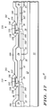
- FIGs. 10-18 illustrate highly enlarged cross-sectional views of a portion of complementary insulated gate field effect transistors 100 during processing in accordance with a second embodiment of the present invention.
- Complementary insulated gate field effect transistors 100 include an N-channel transistor 115 fabricated in a portion of a P-type epitaxial layer 13 and a P-channel transistor 116 fabricated in a portion of an N-well 14.
- FIG. 10 illustrates the partially completed insulated gate field effect transistor 100 after formation of oxide layer 26 and layer of polysilicon 27. It should be noted that the formation of epitaxial layer 13, N-well 14, field implant regions 22 and 23, field oxide regions 24, dopant regions 25 and 30, oxide layer 26 and polysilicon layer 27 have been described with reference to FIG. 1. It should be understood that the locations of N-channel transistor 115 and P-channel transistor 116 in FIGs. 10-18 are included to show the locations of these structures and therefore more clearly describe the invention.
- gate shunt portions 132 and 133 of the gate structures are formed over P-type epitaxial layer 13 and N-well 14, respectively.
- Gate shunt portion 132 having sides 136 and 137 and gate shunt portion 133 having sides 138 and 139 may be formed by anisotropically etching polysilicon layer 27.
- gate shunt portions 132 and 133 are formed by coating polysilicon layer 27 with a layer of photoresist (not shown), exposing the portions of polysilicon layer 27 to be removed (using photolithographic techniques), and anisotropically etching the exposed portions of polysilicon layer 27.
- gate shunt portions 132 and 133 are formed from portions of polysilicon layer 27. It should be understood that gate shunt portions 132 and 133 form part of gate structures 161 and 162, respectively, which are further described in the description of FIG. 16.
- a layer of oxide 141 is formed on gate shunt portions 132 and 133.
- oxide layer 141 is formed by thermally oxidizing gate shunt portions 132 and 133.
- a suitable thickness range for oxide layer 141 is between approximately 50 angstroms and approximately 250 angstroms and a nominal thickness of oxide layer 141 is approximately 100 angstroms.
- the formation of oxide layer 141 by thermal oxidation increases the thicknesses of field oxide regions 24 and oxide layer 26, the increased thicknesses are not shown to simplify the description of the present invention.
- a layer of photoresist 142 having an opening 143, is formed on oxide layer 141, field oxide regions 24 and oxide layer 26. Opening 143 exposes a sub-portion of gate shunt portion 132 and a portion of oxide layer 26 adjacent side 136 of gate shunt portion 132.
- Layer of photoresist 142 serves as an implant block mask.
- an enhanced dopant region 151 is formed by doping a portion of P-type epitaxial layer 13 with an impurity material of P conductivity type such as, for example, boron. More particularly, the boron is implanted into P-type epitaxial layer 13 to form a dopant region 151. It should be noted that dopant region 151 is spaced apart from surface 12.
- a suitable set of implant parameters for forming dopant region 151 includes implanting the boron at a dose in the range of approximately 2 x 10 12 atoms/cm 2 and approximately 2 x 10 13 atoms/cm 2 and an implant energy ranging between approximately 40 KeV and approximately 100 KeV.
- the boron forming dopant region 151 is implanted into P-type epitaxial layer 13 at a depth or distance ranging from approximately 1,500 to 3,000 angstroms.
- the impurity materials forming dopant region 151 serves to provide punch-through protection for N-channel transistor 115.
- An enhanced dopant region 152 is formed by doping another portion of P-type epitaxial layer 13 with boron.
- another implant is performed wherein the boron is implanted into P-type epitaxial layer 13 to a form dopant region 152.
- Suitable implant parameters for the formation of dopant region 152 include implanting the boron at a dose in the range of approximately 5 x 10 11 atoms/cm 2 and approximately 1 x 10 13 atoms/cm 2 and a suitable implant energy ranging between approximately 10 KeV and approximately 20 KeV.
- the boron forming dopant region 152 is implanted into P-type epitaxial layer 13 to a depth or distance ranging from approximately 200 to approximately 1,200 angstroms and serves to adjust the threshold voltage of N-channel transistor 115.
- the layer of photoresist is removed and a layer of photoresist 144, having an opening 145, is formed on oxide layer 141, field oxide regions 24, and portions of oxide layer 26. Opening 145 exposes a subportion of gate shunt portion 133 and a portion of oxide layer 26 adjacent side 138 of gate shunt portion 133.
- Layer of photoresist 144 serves as an implant block mask.
- an enhanced dopant region 153 is formed by doping a portion of N-well 14 with an impurity material of N conductivity type such as, for example, phosphorus. More particularly, the phosphorus is implanted into N-well 14 to form dopant region 153. It should be noted that dopant region 153 is spaced apart from surface 12.
- a suitable set of implant parameters includes implanting the P type impurity material at a dose in the range of approximately 2 x 10 12 atoms/cm 2 and approximately 2 x 10 13 atoms/cm 2 and an implant energy ranging between approximately 40 KeV and approximately 100 KeV.
- the N type impurity material of the implant step that forms dopant region 153 is implanted into N-well 14 to depth or distance ranging from approximately 1,500 to 3,000 angstroms.
- the implant forming dopant region 153 serves to provide punch-through protection for P-channel transistor 116.
- An enhanced dopant region 154 is formed by doping another portion of N-well 14 with phosphorus.
- another implant is performed wherein the impurity material of N conductivity type is implanted into N-well 14 to form dopant region 154.
- Suitable implant parameters for the formation of dopant region 154 include a dose ranging between approximately 5 x 10 11 atoms/cm 2 and approximately 1 x 10 13 atoms/cm 2 and a suitable implant energy ranging between approximately 20 KeV and approximately 40 KeV.
- the N type impurity material of the implant step that forms dopant region 154 is implanted into N-well 14 to a depth or distance ranging from approximately 200 to approximately 1,200 angstroms.
- the implant forming dopant region 154 serves to adjust the threshold voltage of P-channel transistor 116. Layer of photoresist 144 is removed.
- a layer of photoresist 148 having openings 149, is formed on oxide layer 141. Openings 149 expose a sub-portion of gate shunt portion 132, a portion of oxide layer 26 adjacent side 136 of gate shunt portion 132, a sub-portion of gate shunt portion 133, and a portion of oxide layer 26 adjacent side 138 of gate shunt portion 133.
- Layer of photoresist 148 serves as an etch protect mask.
- the exposed portions of oxide layer 26 and oxide layer 141 are isotropically etched using, for example, a wet hydrofluoric acid etch.
- the isotropic etch removes approximately 1,000 angstroms of the exposed portions of oxide layer 26 and portions of oxide layer 26 beneath gate shunt portions 132 and 133, i.e., portion of major surface 12 between and gate shunt portions 132 and 133.
- the isotropic etch undercuts the portions of oxide layer 26 between major surface 12 and gate shunt portions 132 and 133 and forms cavities 135 and 135', respectively, between gate shunt portion 132 and a first portion of major surface 12 and between gate shunt portion 133 and a second portion of major surface 12.
- the isotropic etch removes the exposed portions of oxide layer 141 from gate shunt portions 132 and 133. Layer of photoresist 148 is removed.
- oxide layer 156 is a thin oxide layer having a thickness ranging between approximately 50 angstroms and approximately 150 angstroms. A nominal thickness of oxide layer 156 is approximately 90 angstroms.
- oxide layer 156 is also formed on field oxide regions 24 and oxide layer 26, it should be noted that oxide layer 156 merely thickens or increases the thicknesses of field oxide regions 24 and oxide layer 26. Thus, to simplify the description of the present invention, the portions of oxide layer 156 formed on field oxide regions 24 and oxide layer 26 are not shown.
- oxide layer 156 is also formed on oxide layer 141, to further simplify the description of the second embodiment oxide layers 141 and 156 are shown as a single oxide layer identified by the reference numeral 156.
- a conformal layer of polysilicon 157 having a thickness ranging between approximately 1,000 angstroms and approximately 2,500 angstroms is deposited on oxide layers 24, 26', 41, and on spacers 46 and 47. Nominally, polysilicon layer 157 has a thickness of approximately 1,750 angstroms.
- dopant regions 151 and 152 are initially spaced apart, it should be noted that they diffuse towards each other and form a single dopant region 151'.
- dopant regions 153 and 154 diffuse towards each other and form a single dopant region 153'.
- gate structure 161 comprises a gate shunt portion 132 formed from a first polysilicon portion on the oxide layer 26 of a first width and a gate extension portion 158 formed from a second polysilicon portion on a portion of oxide layer 26' of a second width, wherein the second width is less than the first width.
- gate structure 162 comprises a gate shunt portion 133 formed from a polysilicon portion on the oxide layer 26 of the first width and a gate extension portion 159 formed from a another polysilicon portion on a portion of oxide layer 26' of the second width.
- a layer of photoresist 160 is formed on portions 132 and 133, gate extensions 158 and 159 and the portions of oxide layer 26 adjacent gate extensions 158 and 159.
- gate extensions 158' and 159' and the portions of oxide layer 26 adjacent gate extensions 158' and 159' are exposed.
- Layer of photoresist 160 serves as an etch protect mask.
- Gate extensions 158' and 159' are removed using, for example, an isotropic plasma etch, wherein the isotropic etch stops or endpoints on the exposed portions of oxide layer 26.
- Layer of photoresist 160 is removed.
- a conformal layer of dielectric material 165 is formed on gate shunt portions 132 and 133, gate extensions 158 and 159, and the exposed portions of oxide layer 26.
- layer of dielectric material 165 is a deposited TEOS oxide having a thickness ranging from approximately 100 angstroms to approximately 300 angstroms, and a nominal thickness is 150 angstroms.
- a layer of photoresist (not shown) is formed on the portion of the layer of dielectric material 165 above gate shunt portions 133, gate extension 159 and the portion of major surface 12 of N-well 14.
- the layer of photoresist serves as an implant protect mask preventing P-channel transistor 116 from being doped by a source/drain implant for N-channel transistor 115.
- a source/drain implant is performed to form a source region 163 and a drain region 164.
- the source/drain implant further dopes the gate structure 161.
- a suitable set of implant parameters for the source/drain implant includes implanting an N type impurity material such as arsenic, at a dose ranging between approximately 1 x 10 15 atoms/cm 2 and approximately 1 x 10 16 atoms/cm 2 , and an implant energy ranging between approximately 60 KeV and approximately 160 KeV.
- the layer of photoresist is removed and another layer of photoresist (not shown) is formed on the portions of layer of dielectric material 165 on gate shunt portion 132, extension 158, and the portion of major surface 12 of P-well 13.
- the layer of photoresist serves as an implant protect mask preventing N-channel transistor 115 from being doped by a source/drain implant for P-channel transistor 116.
- a source/drain implant is performed to form a source region 166 and a drain region 167.
- the source/drain implant further dopes the gate structure 162.
- a suitable set of implant parameters for the source/drain implant includes implanting a P type impurity material such as boron, at a dose ranging between approximately 1 X 10 15 atoms/cm 2 and approximately 5 X 10 15 atoms/cm 2 , and an implant energy ranging from approximately 5 KeV to approximately 15 KeV.
- the layer of photoresist is removed.
- An anneal such as, for example, a rapid thermal anneal is performed to anneal any damage caused by the implant and to redistribute the impurity material in the source, drain, and gate regions.
- a conformal layer of dielectric material 169 is formed on layer of oxide layer 165.
- layer of dielectric material 169 is silicon nitride having a thickness ranging between approximately 1,000 angstroms and approximately 2,250 angstroms.
- a nominal thickness of silicon nitride layer 169 is 2,000 angstroms.
- a sequence of anisotropic etches is used to etch silicon nitride layer 169 and oxide layer 165.
- silicon nitride layer 169 is anisotropically etched to form nitride spacers 171, wherein the etching of silicon nitride layer 169 stops on oxide layer 165.
- oxide layer 165 is anisotropically etched to form oxide spacers 170.
- spacers 171 and 170 are formed adjacent sides 136 and 138.
- oxide spacers 170' and nitride spacers 171' are formed in contact with the portions of oxide layer 156 adjacent sides 137 and 139.
- the anisotropic etch step exposes the portions of major surface 12 adjacent spacers 171 and 171' as well as gate shunt portions 132 and 133 and gate extensions 158 and 159 of gate structures 161 and 162, respectively.
- a silicide 176 is formed on dopant region 163
- a silicide 177 is formed on dopant region 164
- a silicide 178 is formed on portions of gate structure 161
- a silicide 179 is formed on dopant region 166
- a silicide 181 is formed on dopant region 167
- a silicide 182 on portions of gate structure 162.
- a layer of dielectric material 184 such as, for example, oxide is formed on field oxide regions 24, spacers 171 and 171', and silicide 176, 177, 178, 179, 181, and 182. Openings are formed in oxide 184 to expose portions of silicide 176, 177, 178, 179, 181, and 182.
- electrical conductors are formed which contact the exposed silicide. More particularly, a source conductor 186 contacts silicide 176, a drain conductor 187 contacts silicide 177, and a gate conductor 188 contacts silicide 178.
- source, drain, and gate conductors, 186, 187, and 188 respectively, form conductors for N-channel transistor 115.
- a source conductor 189 contacts silicide 179
- a drain conductor 191 contacts silicide 181
- a gate conductor 192 contacts silicide 182.
- source, drain, and gate conductors, 189, 191, and 192 form conductors for P-channel transistor 116.
- FIG. 19 illustrates a highly enlarged cross-sectional view of a portion of complementary insulated gate field effect transistors 200 during processing in accordance with a third embodiment of the present invention.
- Complementary insulated gate field effect transistors 200 include an N-channel transistor 215 fabricated in a portion of a P-type epitaxial layer 13 and a buried P-channel transistor 216 fabricated in a portion of an N-well 14.
- the process steps for forming complementary insulated gate field effect transistors 200 follows the steps described for manufacturing complementary insulated gate field effect transistors 10 and 100. However, to form buried P-channel transistor 216, two modifications are made to the processes for forming insulated gate field effect transistors 10 and 100.
- dopant layer 30 is of P conductivity type and has a surface concentration ranging from approximately 7 x 10 16 atoms/cm 3 to approximately 2 x 10 17 atoms/cm 3 .
- a suitable set of implant conditions to obtain the aforementioned surface concentration includes an implant dose ranging from approximately 1 x 10 12 atoms per square centimeter (atoms/cm 2 ) to approximately 3 x 10 12 atoms/cm 2 and an implant energy ranging from approximately 50 kilo-electron volts (KeV) to approximately 200 KeV.
- gate shunt portion 33 and gate extension portion 59 of gate structure 62 are doped with an impurity material of N conductivity type. More particularly, gate structure 62 is doped during the formation of source and drain regions 63 and 64, respectively.
- dopant region 30 is formed at the same time as dopant region 25 and gate shunt portion 33 and gate extension portion 59 are preferably doped at the same time as gate shunt portion 32 and gate extension 58, i.e., gate structures 61 and 62 are preferably doped at the same time.
- a buried P-channel transistor can be manufactured by including a modification to process steps for forming insulated gate field effect transistors 100 that is similar to the process steps for forming insulated gate field effect transistor 10.
- a lightly doped drain extension implant is performed at the beginning stages of manufacture allowing the formation of a gate oxide having a thick portion and a thin portion. Further a gate shunt portion of a gate structure is manufactured on the thick portion of gate oxide and a gate extension is formed on a thin portion of gate oxide.
- the gate shunt portion reduces the gate resistance without significantly increasing the gate capacitance, i.e. gate to drain and gate to substrate capacitances. Further, the thick portion of the gate oxide also decreases the gate capacitance of the device.
- insulated gate semiconductor devices manufactured in accordance with the present invention are at least 50 percent faster than prior art insulated gate semiconductor devices.
- the use of the gate shunt portion allows nonphotolithographic formation of the gate extensions by deposition and etch techniques.
- insulated gate field effect transistors having channel length of less than 0.2 ⁇ m can be manufactured using fabrication facilities designed for devices having gate lengths of 0.5 ⁇ m.
Abstract
Description
- The present invention relates, in general, to insulated gate semiconductor devices, and more particularly, to controlling a threshold voltage, VT, and increasing a transconductance, gm, of insulated gate semiconductor devices.
- As those skilled in the art are aware, VT is related to the voltage at which an insulated gate semiconductor device turns on and varies in accordance with the carrier concentration of the channel region. For example, the gate-source voltage (VGS) of an N-channel insulated gate semiconductor device must exceed VT to form a channel in the insulated gate semiconductor device. Since the voltage at the gate is typically the input voltage of the insulated gate semiconductor device, the input voltage relative to the source voltage must exceed VT for a conducting channel to be formed. In other words, a significant drain current (ID) will not flow through a channel region of the insulated gate semiconductor device unless VGS is greater than VT. In addition, VT is important in determining the saturation current of an insulated gate semiconductor device, which in turn helps determine the power bandwidth of the device.
- Although precise control of VT is highly desirable in all insulated gate semiconductor device applications, it is particularly important in low voltage applications. For insulated gate semiconductor devices using standard power supply levels, the difference between the upper power supply rail (5 volts) and the lower power supply rail (0 volts) is sufficiently large, i.e., approximately 5 volts, that fluctuations in VT have a negligible effect on the device performance. However, in low voltage applications when the difference between the power supply rails is less than 1.5 volts, VT represents a substantial portion of the total power supply voltage. Consequently, fluctuations in VT result in large fluctuations of the current drive capability of the insulated gate semiconductor device.
- In addition, the transconductance, gm, of the insulated gate field effect transistors is influenced by their VGS, ID, and VT. Since the transconductance increases as ID increases, it is desirable to maximize ID, thereby increasing the transconductance. Further, a high frequency switching speed of the insulated gate field effect transistors is reduced by the combination of the gate to drain capacitance and the gate to source capacitances, collectively referred to as gate capacitances. Thus, a large gate capacitance lowers decreases the bandwidth or lowers the frequency response of the insulated gate field effect transistor.
- Accordingly, it would be advantageous to have an insulated gate field effect transistor and method of manufacturing the insulated gate field effect transistor that provides control of the threshold voltage and minimization of the gate capacitance in low voltage, high bandwidth applications.
-
- FIGs. 1-9 illustrate highly enlarged cross-sectional views of a portion of insulated gate field effect transistors during processing in accordance with a first embodiment of the present invention;
- FIGs. 10-18 illustrate highly enlarged cross-sectional views of a portion of insulated gate field effect transistors during processing in accordance with a second embodiment of the present invention; and
- FIG. 19 illustrates a highly enlarged cross-sectional view of insulated gate field effect transistors in accordance with a third embodiment of the present invention.
- Generally, the present invention provides an insulated gate semiconductor device and a method of fabricating or forming the insulated gate semiconductor device. Insulated gate semiconductor devices are also referred to as insulated gate field effect devices and insulated gate field effect transistors. The insulated gate semiconductor devices manufactured in accordance with the present invention have a reduced gate capacitance, thus a higher frequency response or bandwidth, compared to insulated gate semiconductor devices manufactured by other methods. More particularly, the insulated gate semiconductor devices of the present invention have a lightly doped drain (LDD) extension at a drain region of the device which permits formation of a thicker gate dielectric material between the portion of the gate structure adjacent the drain region and the lightly doped drain extension region. Thus, the gate structure comprises two conductive portions: a conductive portion near the drain region of the device which serves as a shunt electrode and an extension, i.e., a second conductive portion, adjacent the source region of the device which serves as an active gate structure.
- It shall be understood that the same reference numerals are used in the figures to denote the same elements. It shall be further understood that the materials, concentrations, and thicknesses provided in the description of the present invention merely serve as examples and are not limitations of the present invention.
- FIG. 1 illustrates an enlarged cross-sectional view of a portion of partially completed complementary insulated gate
field effect transistors 10 during processing in accordance with a first embodiment of the present invention. Complementary insulated gatefield effect transistors 10 include an N-channel transistor 15 fabricated in a portion of a P-typeepitaxial layer 13 and a P-channel transistor 16 fabricated in a portion of an N-well 14. What is shown in FIG. 1 is asubstrate 11 of P conductivity type having anepitaxial layer 13 disposed thereon. By way of example,epitaxial layer 13 is of P conductivity type, has amajor surface 12, and ranges in thickness between approximately 2 microns (µm) and 5 µm. Using methods known in the art, an impurity well 14 of N conductivity type is formed in a portion of P-typeepitaxial layer 13.Substrate 11 has, for example, a resistivity ranging from approximately 0.01 ohm-centimeter (Ω-cm) to approximately 0.1 Ω-cm, and P-typeepitaxial layer 13 has a resistivity between approximately 6 Ω-cm and approximately 8 Ω-cm. P-typeepitaxial layer 13 and N-well 14 have a surface concentration on the order of 5X 10¹⁵ atoms per cubic centimeter (atoms/cm3). Although the description of the present invention includes the combination ofsubstrate 11 and P-typeepitaxial layer 13 to prevent latch-up, it should be understood that insulated gate field effect transistors of the present invention may be manufactured in a semiconductor material such assubstrate 11. In addition,field implant regions 22 are formed in P-typeepitaxial layer 13,field implant regions 23 are formed in N-well 14, andfield oxide regions 24 are formed overfield implant regions - An implant block mask (not shown) such as, for example, photoresist, is formed over N-
well 14 and an impurity material of N conductivity type is implanted into a portion of P-typeepitaxial layer 13 to form adopant layer 25 between two adjacentfield oxide regions 24. Althoughdopant layer 25 is shown as extending across an entire portion of P-typeepitaxial layer 13 between adjacentfield oxide regions 24, it should be understood thatdopant layer 25 may be formed to extend across a subportion of the P-typeepitaxial layer 13 that is between adjacentfield oxide regions 24. The implant block mask is removed and an implant block mask is formed on the P-typeepitaxial layer 13. An impurity material of P conductivity type is implanted into a portion of N-well 14 to form adopant layer 30 between two adjacentfield oxide regions 24. Similar todopant layer 25,dopant layer 30 may be formed to extend across a subportion of N-well 14. It should be noted thatdopant layers epitaxial layer 13 and N-well 14, respectively. Further,dopant layers - By way of example,
layers layers dopant layer 25 ranging from approximately 50 kilo-electron volts (KeV) to approximately 200 KeV; and an implant energy for formingdopant layer 30 ranging from approximately 25 KeV to approximately 100 KeV. - A layer of
dielectric material 26 is formed onmajor surface 12. Although some oxidation procedures increase the thickness offield oxide regions 24 during the formation ofoxide layer 26, to simplify the description of the present invention and because the increase in thickness is small relative to the overall thickness offield oxide regions 24, the increase in the thickness offield oxide region 24 is not shown. A suitable technique for formingoxide layer 26 is thermal oxidation. Preferably,oxide layer 26 has a thickness of at least 400 angstroms. In accordance with the first embodiment of the present invention,oxide layer 26 has a thickness in the range of approximately 600 angstroms to approximately 1,800 angstroms. A typical thickness ofoxide layer 26 is approximately 1,200 angstroms. It should be noted that portions ofoxide layer 26 serve as portions of a gate oxide fortransistors - A layer of
polysilicon 27 is formed onoxide layer 26 using, for example, a chemical vapor deposition technique. A suitable thickness range forpolysilicon layer 27 is from approximately 2,500 angstroms to approximately 4,000 angstroms. A typical thickness forpolysilicon layer 27 is approximately 3,300 angstroms. A layer ofdielectric material 28 is formed onpolysilicon layer 27. For example, layer ofdielectric material 28 is a layer of oxide formed by the decomposition of tetraethyl orthosilicate (TEOS). Oxide layers formed by the decomposition of tetraethyl orthosilicate are commonly referred to as TEOS layers. By way of example,oxide layer 28 has a thickness ranging from approximately 50 angstroms to approximately 400 angstroms and a nominal thickness of approximately 150 angstroms. A layer ofsilicon nitride 29 is formed on layer ofdielectric material 28 using, for example, a low pressure chemical vapor deposition (LPCVD) technique. A suitable range of thicknesses forsilicon nitride layer 29 is between approximately 150 angstroms and approximately 350 angstroms, and nominal thickness forsilicon nitride layer 29 is approximately 250 angstroms. - Now referring to FIG. 2,
portions epitaxial layer 13 and over a portion of N-well 14.Gate shunt portions gate structures portions polysilicon layer 27 and thatportion 32 hassides portion 33 hassides Portions etching nitride layer 29,oxide layer 28, andpolysilicon layer 27.Gate shunt portions silicon nitride layer 29 with a layer of photoresist (not shown), exposing the portions ofsilicon nitride layer 29 to be removed (using, for example, photolithographic techniques), and anisotropically etching the exposed portions ofsilicon nitride layer 29. In addition, the portions ofoxide layer 28 andpolysilicon layer 27 below the exposed portions ofsilicon nitride layer 29 are also etched, thereby exposing portions ofoxide layer 26 andfield oxide regions 24. - Now referring to FIG. 3, a layer of
oxide 41 is formed on exposedsides gate shunt portions oxide layer 41 is formed by thermally oxidizing thesides oxide layer 41 is between approximately 50 angstroms and approximately 250 angstroms, and a nominal thickness ofoxide layer 41 is approximately 100 angstroms. Although the formation ofoxide layer 41 by thermal oxidization increases the thicknesses offield oxide regions 24 andoxide layer 26, the increased thicknesses oflayers - A conformal layer of
dielectric material 43 is formed ongate shunt portions oxide layer 26 andfield oxide regions 24. By way of example, layer ofdielectric material 43 is silicon nitride having a thickness ranging from approximately 250 angstroms to approximately 750 angstroms, and a nominal thickness of approximately 400 angstroms. It should be noted that the impurity materials of dopant layers 25 and 30 are activated or driven into P-type epitaxial layer 13 and N-well 14, respectively, by the processing steps described supra. - Now referring to FIG. 4,
silicon nitride layer 43 is anisotropically etched to formspacers adjacent oxide layer 41. A suitable technique for etchingsilicon nitride layer 43 includes a reactive ion etch (RIE) using etchants such as CF4, NF3, and the like. In addition, the anisotropic etch step may remove a portion ofoxide layer 26. For example,oxide layer 26 is thinned to approximately 400 angstroms after the formation ofspacers spacers oxide layer 26 and that spacers 46' and 47'shape oxide layer 26 in order to create a repeatable undercut etch profile (shown in FIG. 5). - Now referring to FIG. 5, a layer of photoresist (not shown) is formed on subportions of
gate shunt portions spacers oxide layers oxide layer 26 betweengate shunt portion 32 and a first portion ofmajor surface 12 as well as the portion ofoxide layer 26 betweengate shunt portion 33 and a second portion ofmajor surface 12. In other words,gate shunt portions cavity 35 underneathgate shunt portion 32, i.e., betweengate shunt portion 32 and the first portion ofmajor surface 12 and a cavity 35' underneathgate shunt portion 33, i.e., betweengate shunt portion 33 and the second portion ofmajor surface 12. The layer of photoresist is removed. - Still referring to FIG. 5, a
screen oxide 40 is formed on the exposed portions ofgate shunt portions major surface 12. By way of example,oxide layer 40 has a thickness ranging from approximately 100 angstroms to approximately 200 angstroms, with a nominal thickness of approximately 150 angstroms. Althoughoxide layer 40 is also formed onfield oxide regions 24 andoxide layer 26, it should be noted that to simplify the description of the present invention, these portions ofoxide layer 40 are not shown. A layer of photoresist (not shown) is formed on portions ofoxide 40 disposed ongate shunt portions spacers oxide layer 40adjacent sides field oxide regions 24. This layer of photoresist serves as an implant block mask. - An
enhanced dopant region 51 is formed by doping a portion of P-type epitaxial layer 13 with an impurity material of P conductivity type such as, for example, boron. More particularly, the boron is implanted into a portion of P-type epitaxial layer 13 to formdopant region 51.Dopant region 51 is laterally aligned to fieldoxide region 24 of N-channel transistor 15 andoxide layer 40 disposed onside 36 ofgate shunt portion 32. It should be noted thatdopant region 51 is spaced apart frommajor surface 12. A suitable set of implant parameters includes implanting the P type impurity material at a dose ranging from approximately 2 x 10¹² atoms/cm2 to approximately 2 x 10¹³ atoms/cm2 at an implant energy ranging from approximately 40 KeV to approximately 100 KeV. Thus, the boron that formsdopant region 51 is implanted into P-type epitaxial layer 13 to a depth or distance ranging between approximately 1,500 and approximately 3,000 angstroms. The impurity materials or dopant formingdopant region 51 serves to provide punch-through protection for N-channel transistor 15. - An
enhanced dopant region 52 is formed by doping another portion of P-type epitaxial layer 13 with boron. By way of example, implant parameters for the formation ofdopant region 52 include a dose ranging from approximately 5 x 10¹¹ atoms/cm2 to approximately 1 x 10¹³ atoms/cm2 and a suitable implant energy ranging from approximately 10 KeV to approximately 20 KeV. Thus the boron that formsdopant region 52 is implanted into a portion of P-type epitaxial layer 13 to a depth or distance ranging from approximately 200 to approximately 1,200 angstroms. The impurity materials formingdopant region 52 serves to adjust the threshold voltage of N-channel transistor 15. The layer of photoresist is removed and a layer of photoresist (not shown) is formed on portions ofscreen oxide 40 disposed ongate shunt portions spacer 47, portions ofoxide layer 26adjacent spacer 47, portions ofoxide layer 26 over P-type epitaxial layer 13, and portions offield oxide regions 24. This layer of photoresist also serves as an implant block mask. - An
enhanced dopant region 53 is formed by doping a portion of N-well 14 with an impurity material of N conductivity type such as, for example, phosphorus. More particularly, the phosphorus is implanted into N-well 14 to formdopant region 53. It should be noted thatdopant region 53 is spaced apart fromsurface 12. A suitable set of implant parameters includes implanting the N type impurity material at a dose ranging from approximately 2 x 10¹² atoms/cm2 to approximately 2 x 10¹³ atoms/cm2 at an implant energy ranging from approximately 80 KeV to approximately 200 KeV. Thus, the N type impurity material of the implant step that formsdopant region 53 is implanted into N-well 14 to a depth or distance ranging from approximately 1,500 to approximately 3,000 angstroms. The impurity materials formingdopant region 53 serves to provide punch-through protection for P-channel transistor 16. - An
enhanced dopant region 54 is formed by doping another portion of N-well 14 with phosphorus. By way of example, the boron is implanted into N-well 14 to formdopant region 54. Suitable implant parameters for the formation ofdopant region 54 include a dose ranging from approximately 5 x 10¹¹ atoms/cm2 to approximately 1 x 10¹³ atoms/cm2 and a suitable implant energy ranging from approximately 20 KeV to approximately 40 KeV. Thus, the N type impurity material of the implant step that formsdopant region 54 is implanted into N-well 14 to a depth or distance ranging from approximately 200 to 1,200 angstroms. The impurity materials formingdopant region 54 serves to adjust the threshold voltage of P-channel transistor 16. The layer of photoresist is removed. - Now referring to FIG. 6,
screen oxide 40 is removed fromgate shunt portions major surface 12, thereby exposing subportions ofgate shunt portions major surface 12 and forming oxide extensions 55. An oxide layer 26' is formed on the exposed portions ofmajor surface 12 and the exposed regions ofgate shunt portions - One of a layer of semiconductor material or a
conductor material 57 including, for example, amorphous silicon, single crystal silicon, polysilicon, tungsten, or the like, is formed onoxide layers 24, 26', the remaining portions ofoxide layer 41, andspacers polysilicon 57 having a thickness ranging between approximately 1,000 angstroms and approximately 2,500 angstroms is deposited onoxide layers spacers polysilicon layer 57 has a thickness of approximately 1,750 angstroms. Althoughdopant regions dopant regions - Now referring to FIG. 7,
polysilicon layer 57 is anisotropically etched to formgate extensions adjacent sides gate extensions respective sides adjacent spacers gate extensions gate structure 61 comprises agate shunt portion 32 formed from a first polysilicon portion on theoxide layer 26 of a first width and agate extension portion 58 formed from a second polysilicon portion on a portion of oxide layer 26' of a second width, wherein the second width is less than the first width. Likewise,gate structure 62 comprises agate shunt portion 33 formed from a polysilicon portion on theoxide layer 26 of the first width and agate extension portion 59 formed from a another polysilicon portion on a portion of oxide layer 26' of the second width. - Now referring to FIG. 8, a layer of photoresist (not shown) is formed on
gate shunt portions gate extensions adjacent gate extensions spacers spacers - It should be understood that
gate extension 58 cooperates withgate shunt portion 32 and the portions of oxide layer 26' on P-type epitaxial layer 13 to form agate structure 61. Likewise, it should be understood thatgate extension 59 cooperates withgate shunt portion 33 and a portion of oxide layer 26' on N-well 14 to formgate structure 62. The portions of oxide layer 26' betweengate extension 58 andmajor surface 12 and betweengate extension 59 andmajor surface 12 serve as active gate oxide. - An
oxide layer 60 is conformally deposited onfield oxide regions 24, and the remaining portions of oxide layer 26',oxide layer 41,spacers gate extensions oxide layer 60 has a thickness ranging from approximately 100 angstroms to approximately 300 angstroms, wherein a nominal thickness ofoxide layer 60 is approximately 150 angstroms. - A layer of photoresist (not shown) is formed on the portions of the layer of
dielectric material 60 overgate structures oxide layer 60 over N-well 14 that are adjacent togate structure 62. In other words the layer of photoresist serves as an implant protect mask preventing P-channel transistor 16 from being doped by a source/drain implant for N-channel transistor 15. A source/drain implant is performed to form asource region 63 and adrain region 64. In addition, the source/drain implant further dopesgate structure 61. A suitable set of implant parameters for the source/drain implant includes implanting an N type impurity material such as arsenic, at a dose in the range of approximately 1 x 10¹⁵ atoms/cm2 to approximately 1 x 10¹⁶ atoms/cm2, and a suitable implant energy ranges from approximately 60 KeV to approximately 120 KeV. - The layer of photoresist is removed and another layer of photoresist (not shown) is formed on the portion of the layer of
dielectric material 60 abovegate structures oxide layer 60 over P-type epitaxial layer 13adjacent gate structure 61. In other words the layer of photoresist serves as an implant protect mask preventing N-channel transistor 15 from being doped by a source/drain implant of the P-channel transistor 16. A source/drain implant of, for example, boron is performed to form asource region 66 and adrain region 67. In addition, the source/drain implant further dopesgate structure 62. A suitable set of implant parameters for the source/drain implant includes implanting a P type impurity material such as boron, at a dose in the range of approximately 1 X 10¹⁵ atoms/cm2 to approximately 5 X 10¹⁵ atoms/cm2, and a suitable implant energy ranges from approximately 5 KeV to approximately 15 KeV. The layer of photoresist is removed. - Still referring to FIG. 8, a conformal layer of
dielectric material 69 is formed on layer ofdielectric material 60. By way of example, layer ofdielectric material 69 is silicon nitride having a thickness ranging from approximately 1,000 angstroms to approximately 2,250 angstroms. A nominal thickness ofsilicon nitride layer 69 is 2,000 angstroms. - Now referring to FIG. 9,
silicon nitride layer 69 andoxide layer 60 are anisotropically etched to formoxide spacers 70 andnitride spacers 71adjacent sides spacers gate shunt portions gate extensions gate structures major surface 12adjacent spacers 71 and 71'. Using techniques well known in the art, asilicide 76 is formed ondopant region 63, asilicide 77 is formed ondopant region 64, asilicide 78 is formed on portions ofgate structure 61, asilicide 79 is formed ondopant region 66, asilicide 81 is formed ondopant region 67, and asilicide 82 on portions ofgate structure 62. It should be noted thatsilicide 78 serves as a conductive strap couplinggate shunt portion 32 togate extension 58 andsilicide 82 serves as a conductive strap couplinggate shunt portion 33 togate extension 59. - A layer of
dielectric material 84, such as, for example, oxide is formed onfield oxide regions 24,spacers 71 and 71', andsilicide oxide layer 84 to expose portions ofsilicide silicide source conductor 86contacts silicide 76, adrain conductor 87contacts silicide 77, and a gate conductor 88contacts silicide 78. Thus, source, drain, and gate conductors, 86, 87, and 88, respectively, form conductors for N-channel transistor 15. Likewise, asource conductor 89contacts silicide 79, adrain conductor 91contacts silicide 81, and agate conductor 92contacts silicide 82. Thus, source, drain, and gate conductors, 89, 91, and 92, respectively, form conductors for P-channel transistor 16. It should be understood thatgate conductors 88 and 92 are highly simplified illustrations to show a gate conductor electrically coupled to a gate structure. - FIGs. 10-18 illustrate highly enlarged cross-sectional views of a portion of complementary insulated gate
field effect transistors 100 during processing in accordance with a second embodiment of the present invention. Complementary insulated gatefield effect transistors 100 include an N-channel transistor 115 fabricated in a portion of a P-type epitaxial layer 13 and a P-channel transistor 116 fabricated in a portion of an N-well 14. FIG. 10 illustrates the partially completed insulated gatefield effect transistor 100 after formation ofoxide layer 26 and layer ofpolysilicon 27. It should be noted that the formation ofepitaxial layer 13, N-well 14,field implant regions field oxide regions 24,dopant regions oxide layer 26 andpolysilicon layer 27 have been described with reference to FIG. 1. It should be understood that the locations of N-channel transistor 115 and P-channel transistor 116 in FIGs. 10-18 are included to show the locations of these structures and therefore more clearly describe the invention. - Now referring to FIG. 11,
gate shunt portions type epitaxial layer 13 and N-well 14, respectively.Gate shunt portion 132 havingsides gate shunt portion 133 havingsides polysilicon layer 27. By way of example,gate shunt portions polysilicon layer 27 with a layer of photoresist (not shown), exposing the portions ofpolysilicon layer 27 to be removed (using photolithographic techniques), and anisotropically etching the exposed portions ofpolysilicon layer 27. Thus,gate shunt portions polysilicon layer 27. It should be understood thatgate shunt portions gate structures - Still referring to FIG. 11, a layer of
oxide 141 is formed ongate shunt portions oxide layer 141 is formed by thermally oxidizinggate shunt portions oxide layer 141 is between approximately 50 angstroms and approximately 250 angstroms and a nominal thickness ofoxide layer 141 is approximately 100 angstroms. Although, the formation ofoxide layer 141 by thermal oxidation increases the thicknesses offield oxide regions 24 andoxide layer 26, the increased thicknesses are not shown to simplify the description of the present invention. - A layer of
photoresist 142, having anopening 143, is formed onoxide layer 141,field oxide regions 24 andoxide layer 26.Opening 143 exposes a sub-portion ofgate shunt portion 132 and a portion ofoxide layer 26adjacent side 136 ofgate shunt portion 132. Layer ofphotoresist 142 serves as an implant block mask. In accordance with the second embodiment, anenhanced dopant region 151 is formed by doping a portion of P-type epitaxial layer 13 with an impurity material of P conductivity type such as, for example, boron. More particularly, the boron is implanted into P-type epitaxial layer 13 to form adopant region 151. It should be noted thatdopant region 151 is spaced apart fromsurface 12. A suitable set of implant parameters for formingdopant region 151 includes implanting the boron at a dose in the range of approximately 2 x 10¹² atoms/cm2 and approximately 2 x 10¹³ atoms/cm2 and an implant energy ranging between approximately 40 KeV and approximately 100 KeV. Thus, the boron formingdopant region 151 is implanted into P-type epitaxial layer 13 at a depth or distance ranging from approximately 1,500 to 3,000 angstroms. The impurity materials formingdopant region 151 serves to provide punch-through protection for N-channel transistor 115. - An
enhanced dopant region 152 is formed by doping another portion of P-type epitaxial layer 13 with boron. By way of example, another implant is performed wherein the boron is implanted into P-type epitaxial layer 13 to aform dopant region 152. Suitable implant parameters for the formation ofdopant region 152 include implanting the boron at a dose in the range of approximately 5 x 10¹¹ atoms/cm2 and approximately 1 x 10¹³ atoms/cm2 and a suitable implant energy ranging between approximately 10 KeV and approximately 20 KeV. Thus, the boron formingdopant region 152 is implanted into P-type epitaxial layer 13 to a depth or distance ranging from approximately 200 to approximately 1,200 angstroms and serves to adjust the threshold voltage of N-channel transistor 115. - Now referring to FIG. 12, the layer of photoresist is removed and a layer of
photoresist 144, having anopening 145, is formed onoxide layer 141,field oxide regions 24, and portions ofoxide layer 26.Opening 145 exposes a subportion ofgate shunt portion 133 and a portion ofoxide layer 26adjacent side 138 ofgate shunt portion 133. Layer ofphotoresist 144 serves as an implant block mask. - In accordance with the second embodiment of the present invention, an
enhanced dopant region 153 is formed by doping a portion of N-well 14 with an impurity material of N conductivity type such as, for example, phosphorus. More particularly, the phosphorus is implanted into N-well 14 to formdopant region 153. It should be noted thatdopant region 153 is spaced apart fromsurface 12. A suitable set of implant parameters includes implanting the P type impurity material at a dose in the range of approximately 2 x 10¹² atoms/cm2 and approximately 2 x 10¹³ atoms/cm2 and an implant energy ranging between approximately 40 KeV and approximately 100 KeV. Thus, the N type impurity material of the implant step that formsdopant region 153 is implanted into N-well 14 to depth or distance ranging from approximately 1,500 to 3,000 angstroms. The implant formingdopant region 153 serves to provide punch-through protection for P-channel transistor 116. - An
enhanced dopant region 154 is formed by doping another portion of N-well 14 with phosphorus. By way of example, another implant is performed wherein the impurity material of N conductivity type is implanted into N-well 14 to formdopant region 154. Suitable implant parameters for the formation ofdopant region 154 include a dose ranging between approximately 5 x 10¹¹ atoms/cm2 and approximately 1 x 10¹³ atoms/cm2 and a suitable implant energy ranging between approximately 20 KeV and approximately 40 KeV. Thus, the N type impurity material of the implant step that formsdopant region 154 is implanted into N-well 14 to a depth or distance ranging from approximately 200 to approximately 1,200 angstroms. The implant formingdopant region 154 serves to adjust the threshold voltage of P-channel transistor 116. Layer ofphotoresist 144 is removed. - Now referring to FIG. 13, a layer of
photoresist 148, havingopenings 149, is formed onoxide layer 141.Openings 149 expose a sub-portion ofgate shunt portion 132, a portion ofoxide layer 26adjacent side 136 ofgate shunt portion 132, a sub-portion ofgate shunt portion 133, and a portion ofoxide layer 26adjacent side 138 ofgate shunt portion 133. Layer ofphotoresist 148 serves as an etch protect mask. - The exposed portions of
oxide layer 26 andoxide layer 141 are isotropically etched using, for example, a wet hydrofluoric acid etch. In accordance with the second embodiment, the isotropic etch removes approximately 1,000 angstroms of the exposed portions ofoxide layer 26 and portions ofoxide layer 26 beneathgate shunt portions major surface 12 between andgate shunt portions oxide layer 26 betweenmajor surface 12 andgate shunt portions forms cavities 135 and 135', respectively, betweengate shunt portion 132 and a first portion ofmajor surface 12 and betweengate shunt portion 133 and a second portion ofmajor surface 12. In addition, the isotropic etch removes the exposed portions ofoxide layer 141 fromgate shunt portions photoresist 148 is removed. - Now referring to FIG. 14, a layer of
oxide 156 is formed ongate shunt portions oxide layer 156 is a thin oxide layer having a thickness ranging between approximately 50 angstroms and approximately 150 angstroms. A nominal thickness ofoxide layer 156 is approximately 90 angstroms. Although,oxide layer 156 is also formed onfield oxide regions 24 andoxide layer 26, it should be noted thatoxide layer 156 merely thickens or increases the thicknesses offield oxide regions 24 andoxide layer 26. Thus, to simplify the description of the present invention, the portions ofoxide layer 156 formed onfield oxide regions 24 andoxide layer 26 are not shown. Althoughoxide layer 156 is also formed onoxide layer 141, to further simplify the description of the second embodiment oxide layers 141 and 156 are shown as a single oxide layer identified by thereference numeral 156. - One of a layer of semiconductor material or a
conductor material 157 including, for example, amorphous silicon, single crystal silicon, polysilicon, tungsten, or the like, is formed onoxide layers 24, 26', the remaining portions ofoxide layer 41, andspacers polysilicon 157 having a thickness ranging between approximately 1,000 angstroms and approximately 2,500 angstroms is deposited onoxide layers spacers polysilicon layer 157 has a thickness of approximately 1,750 angstroms. Althoughdopant regions dopant regions - Now referring to FIG. 15,
polysilicon layer 157 is anisotropically etched to formgate extensions adjacent sides sides gate structure 161 comprises agate shunt portion 132 formed from a first polysilicon portion on theoxide layer 26 of a first width and agate extension portion 158 formed from a second polysilicon portion on a portion of oxide layer 26' of a second width, wherein the second width is less than the first width. Likewise,gate structure 162 comprises agate shunt portion 133 formed from a polysilicon portion on theoxide layer 26 of the first width and agate extension portion 159 formed from a another polysilicon portion on a portion of oxide layer 26' of the second width. - Now referring to FIG. 16, a layer of
photoresist 160 is formed onportions gate extensions oxide layer 26adjacent gate extensions oxide layer 26 adjacent gate extensions 158' and 159' are exposed. Layer ofphotoresist 160 serves as an etch protect mask. Gate extensions 158' and 159' are removed using, for example, an isotropic plasma etch, wherein the isotropic etch stops or endpoints on the exposed portions ofoxide layer 26. Layer ofphotoresist 160 is removed. - Now referring to FIG. 17, a conformal layer of
dielectric material 165 is formed ongate shunt portions gate extensions oxide layer 26. By way of example layer ofdielectric material 165 is a deposited TEOS oxide having a thickness ranging from approximately 100 angstroms to approximately 300 angstroms, and a nominal thickness is 150 angstroms. A layer of photoresist (not shown) is formed on the portion of the layer ofdielectric material 165 abovegate shunt portions 133,gate extension 159 and the portion ofmajor surface 12 of N-well 14. In other words, the layer of photoresist serves as an implant protect mask preventing P-channel transistor 116 from being doped by a source/drain implant for N-channel transistor 115. A source/drain implant is performed to form asource region 163 and adrain region 164. In addition, the source/drain implant further dopes thegate structure 161. A suitable set of implant parameters for the source/drain implant includes implanting an N type impurity material such as arsenic, at a dose ranging between approximately 1 x 10¹⁵ atoms/cm2 and approximately 1 x 10¹⁶ atoms/cm2, and an implant energy ranging between approximately 60 KeV and approximately 160 KeV. - The layer of photoresist is removed and another layer of photoresist (not shown) is formed on the portions of layer of
dielectric material 165 ongate shunt portion 132,extension 158, and the portion ofmajor surface 12 of P-well 13. In other words the layer of photoresist serves as an implant protect mask preventing N-channel transistor 115 from being doped by a source/drain implant for P-channel transistor 116. A source/drain implant is performed to form asource region 166 and adrain region 167. In addition, the source/drain implant further dopes thegate structure 162. A suitable set of implant parameters for the source/drain implant includes implanting a P type impurity material such as boron, at a dose ranging between approximately 1 X 10¹⁵ atoms/cm2 and approximately 5 X 10¹⁵ atoms/cm2, and an implant energy ranging from approximately 5 KeV to approximately 15 KeV. The layer of photoresist is removed. An anneal such as, for example, a rapid thermal anneal is performed to anneal any damage caused by the implant and to redistribute the impurity material in the source, drain, and gate regions. - Still referring to FIG. 17, a conformal layer of
dielectric material 169 is formed on layer ofoxide layer 165. By way of example, layer ofdielectric material 169 is silicon nitride having a thickness ranging between approximately 1,000 angstroms and approximately 2,250 angstroms. A nominal thickness ofsilicon nitride layer 169 is 2,000 angstroms. - Now referring to FIG. 18, a sequence of anisotropic etches is used to etch
silicon nitride layer 169 andoxide layer 165. For example,silicon nitride layer 169 is anisotropically etched to formnitride spacers 171, wherein the etching ofsilicon nitride layer 169 stops onoxide layer 165. Thenoxide layer 165 is anisotropically etched to formoxide spacers 170. Thus,spacers adjacent sides oxide layer 156adjacent sides major surface 12adjacent spacers 171 and 171' as well asgate shunt portions gate extensions gate structures silicide 176 is formed ondopant region 163, asilicide 177 is formed ondopant region 164, asilicide 178 is formed on portions ofgate structure 161, asilicide 179 is formed ondopant region 166, asilicide 181 is formed ondopant region 167, and asilicide 182 on portions ofgate structure 162. - A layer of
dielectric material 184, such as, for example, oxide is formed onfield oxide regions 24,spacers 171 and 171', andsilicide oxide 184 to expose portions ofsilicide source conductor 186 contacts silicide 176, adrain conductor 187 contacts silicide 177, and agate conductor 188 contacts silicide 178. Thus, source, drain, and gate conductors, 186, 187, and 188, respectively, form conductors for N-channel transistor 115. Likewise, asource conductor 189 contacts silicide 179, adrain conductor 191 contacts silicide 181, and agate conductor 192 contacts silicide 182. Thus, source, drain, and gate conductors, 189, 191, and 192, respectively, form conductors for P-channel transistor 116. - FIG. 19 illustrates a highly enlarged cross-sectional view of a portion of complementary insulated gate
field effect transistors 200 during processing in accordance with a third embodiment of the present invention. Complementary insulated gatefield effect transistors 200 include an N-channel transistor 215 fabricated in a portion of a P-type epitaxial layer 13 and a buried P-channel transistor 216 fabricated in a portion of an N-well 14. The process steps for forming complementary insulated gatefield effect transistors 200 follows the steps described for manufacturing complementary insulated gatefield effect transistors channel transistor 216, two modifications are made to the processes for forming insulated gatefield effect transistors dopant layer 30 is of P conductivity type and has a surface concentration ranging from approximately 7 x 10¹⁶ atoms/cm3 to approximately 2 x 10¹⁷ atoms/cm3. A suitable set of implant conditions to obtain the aforementioned surface concentration includes an implant dose ranging from approximately 1 x 10¹² atoms per square centimeter (atoms/cm2) to approximately 3 x 10¹² atoms/cm2 and an implant energy ranging from approximately 50 kilo-electron volts (KeV) to approximately 200 KeV. - In the second modification (and referring to the processing steps for manufacturing insulated gate field effect transistors 10),
gate shunt portion 33 andgate extension portion 59 ofgate structure 62 are doped with an impurity material of N conductivity type. More particularly,gate structure 62 is doped during the formation of source and drainregions dopant region 30 is formed at the same time asdopant region 25 andgate shunt portion 33 andgate extension portion 59 are preferably doped at the same time asgate shunt portion 32 andgate extension 58, i.e.,gate structures field effect transistors 100 that is similar to the process steps for forming insulated gatefield effect transistor 10. - By now it should be appreciated that an insulated gate semiconductor device and a method manufacturing the insulated gate semiconductor device have been provided. In accordance with the present invention, a lightly doped drain extension implant is performed at the beginning stages of manufacture allowing the formation of a gate oxide having a thick portion and a thin portion. Further a gate shunt portion of a gate structure is manufactured on the thick portion of gate oxide and a gate extension is formed on a thin portion of gate oxide. The gate shunt portion reduces the gate resistance without significantly increasing the gate capacitance, i.e. gate to drain and gate to substrate capacitances. Further, the thick portion of the gate oxide also decreases the gate capacitance of the device. The decrease in a gate to drain portion of the gate capacitance decreases a "Miller multiplied" capacitance, thereby increasing the frequency response of the devices of the present invention. It has been determined that insulated gate semiconductor devices manufactured in accordance with the present invention are at least 50 percent faster than prior art insulated gate semiconductor devices. In addition, the use of the gate shunt portion allows nonphotolithographic formation of the gate extensions by deposition and etch techniques. Thus, insulated gate field effect transistors having channel length of less than 0.2 µm can be manufactured using fabrication facilities designed for devices having gate lengths of 0.5 µm.
Claims (10)
- A method for fabricating an insulated gate semiconductor device, comprising the steps of:providing a semiconductor material (13) of a first conductivity type and having a major surface (12);forming a first dopant layer (25) extending from the major surface (12) into the semiconductor material (13);forming a first portion (32) of a first gate structure (61) on a first portion of a first layer of dielectric material (26), the first portion (32) of the first gate structure (61) having first (36) and second (37) sides and spaced apart from the major surface (12) by the first portion of the first layer of dielectric material (26);doping at least one portion of the semiconductor material (13) adjacent the first side (36) of the first portion (32) of the first gate structure (61) with impurities of the first conductivity type;laterally removing a subportion of the first portion of the first layer of dielectric material (26) to form a first cavity (35), the first cavity (35) extending between the first portion (32) of the first gate structure (61) and the major surface (12) from the first side (36);forming a second layer of dielectric material (26') adjacent at least the first portion (32) of the first gate structure (61);forming a second portion (58) of the first gate structure (61), the second portion (58) of the first gate structure (61) spaced apart from the first side (36) of the first gate structure (61) by the second layer of dielectric material (26') filling a portion of the first cavity (35);doping a portion (64) of the semiconductor material (13) adjacent the second side (37) of the first portion (32) of the first gate structure (61) and a portion (63) of the semiconductor material (13) adjacent the second side of the second portion (58) of the first gate structure (61); anddoping a portion of the first gate structure (61).
- The method of claim 1, wherein the step of laterally removing a subportion of the first portion of the first layer of dielectric material (26) to form a first cavity (35) includes exposing the first side (36) of the first portion (32) of the first gate structure (61).
- The method of claim 1, further including the steps of:forming a dopant well (14) of a second conductivity type in a portion of the semiconductor material (13);forming a second dopant layer (30) extending from the major surface (12) into the dopant well (14);forming a first portion (33) of a second gate structure (62) on a second portion of a first layer of dielectric material, the first portion (33) of the second gate structure (62) having first (38) and second (39) sides and spaced apart from the major surface (12) by the second portion of the first layer of dielectric material (26);doping at least one portion of the dopant well (14) adjacent the first side (38) of the first portion (33) of the first gate structure with impurities of the first conductivity type;laterally removing a subportion of the second portion of the first layer of dielectric material (26) to form a second cavity (35'), the second cavity (35') extending between the first portion (33) of the second gate structure (62) and the major surface (12) from the first side (38);forming a third layer of dielectric material adjacent at least the first portion (33) of the second gate structure (62);forming a second portion (59) of the second gate structure (62), the second portion (59) of the second gate structure (62) spaced apart from the first side (38) of the second gate structure (62) by the third layer of dielectric material filling a portion of the second cavity (35');doping a portion of the dopant well (14) adjacent the second side (39) of the first portion (33) of the second gate structure (62) and a portion of the dopant well (14) adjacent the second side of the second portion (59) of the second gate structure (62); anddoping a portion of the second gate structure (62).
- A method of forming an insulated gate semiconductor device, comprising the steps of:providing a semiconductor material (13) of a first conductivity type and having a major surface (12);forming a first dopant layer (25) of a second conductivity type extending from the major surface (12) into the semiconductor material (13);forming a first layer of dielectric material (26) on the major surface (12);forming a first portion (32) of a first gate structure (61) on a first portion of the first layer of dielectric material (26), the first portion (32) of the first gate structure (61) having first (36) and second (37) sides and a top surface (45);forming a first cavity (35) extending under the first portion (32) of the first gate structure (61) from the first side (36) and exposing a portion of the major surface (12);forming at least one enhanced dopant region (51) of the first conductivity type in the semiconductor material (13), the at least one enhanced dopant region (51) aligned to the first side (36) of the first portion (32) of the first gate structure (61);forming a second layer of dielectric material (26') on the first gate structure (61) and the portion of the major surface (12) that is exposed;forming a second portion (58) of the first gate structure (61) on the second layer of dielectric material (26'), the second portion (58) of the first gate structure (61) having first and second sides and the second side of the second portion (58) of the first gate structure (61) adjacent the first side (36) of the first portion (32) of the first gate structure (61);forming first (63) and second (64) dopant regions of the second conductivity type, the first dopant region (63) aligned to the first side of the second portion (58) of the first gate structure (61) and the second dopant region (64) aligned to the second side (37) of the first portion (32) of the first gate structure (61);doping the first (32) and second (58) portions of the first gate structure (61) with impurities of the second conductivity type; andforming a first conductive strap (78) which couples the first (32) and second (58) portions of the first gate structure (61).
- The method of claim 4, further including the steps of:forming a second layer of dielectric material (26') on the first portion (32) of the first gate structure (61) and portions of the first layer of dielectric material (26) adjacent the first gate structure (61);anisotropically etching the second layer of dielectric material (26') to form a plurality of spacers adjacent the first portion (32) of the first gate structure (61);removing a portion of the first layer of dielectric material (26); andremoving a first spacer (71) of the plurality of spacers to form an oxide extension, the first spacer (71) adjacent the first side (36) of the first portion (32) of the first gate structure (61).
- The method of claim 4, wherein the step of forming a second portion (58) of the first gate structure (61) includes depositing one (57) of a semiconductor material or a conductor material on the second layer of dielectric material (26'), wherein the one (57) of a semiconductor material or a conductor material fills a portion of the first cavity (35).
- The method of claim 6, wherein the one (57) of a semiconductor material or a conductor material is selected from a group consisting of polysilicon, amorphous silicon, single crystal silicon, and tungsten.
- An insulated gate semiconductor device, comprising:a semiconductor material (13) of a first conductivity type and having a major surface (12);a first layer of dielectric material (26) on the semiconductor material (13);a dopant layer (25) of a second conductivity type extending from the major surface (12) into a first portion of the semiconductor material (13);a first gate structure (61) having first (32) and second (58) conductive portions, the first conductive portion (32) of the first gate structure (61) on a first portion of the first layer of dielectric material (26) and having first (36) and second (37) sides, the second conductive portion (58) of the first gate structure (61) having first and second sides, wherein a second side of the second conductive portion (58) of the first gate structure (61) is spaced apart from the first side (36) of the first conductive portion (32) of the first gate structure (61) by a second layer of dielectric material (26') and a subportion of the second conductive portion (58) of the first gate structure (61) between the first portion (32) of the first gate structure (61) and a portion of the major surface (12);at least one enhanced dopant region (51) of the first conductivity type, the at least one enhanced dopant region (51) in at least a portion of the semiconductor material (13) beneath the second conductive portion (58) of the first gate structure (61); andfirst (64) and second (63) dopant regions of the second conductivity type, the first dopant region (64) in a portion of the semiconductor material (13) adjacent the second side (37) of the first portion (32) of the first gate structure (61), the second dopant region (63) in a portion of the semiconductor material (13) adjacent the first side of the second conductive portion (58) of the first gate structure (61).
- The insulated gate semiconductor device of claim 8 further including:a dopant well (14) of the second conductivity type extending into a second portion of the semiconductor material (13) from the major surface (12);a dopant layer (30) of the first conductivity type extending from the major surface (12) into the dopant well (14);a second gate structure (62) having first (33) and second (59) conductive portions, the first conductive portion (33) of the second gate structure (62) on a second portion of the first layer of dielectric material (26) and having first (38) and second (39) sides, the second conductive portion (59) of the second gate structure (62) having first and second sides, wherein a second side of the second portion (59) of the second gate structure (62) is spaced apart from the first side of the second gate structure (62) by a third layer of dielectric material and a subportion of the second portion (59) of the second gate structure (62) between the first portion (33) the second gate structure (62) and a portion of the major surface (12);at least one enhanced dopant region (53) of the second conductivity type, the at least one enhanced dopant region (53) in at least a portion of the dopant well (14) beneath the second conductive portion of the second gate structure (62); andthird (67) and fourth (66) dopant regions of the first conductivity type, the third dopant region (67) in a portion of the dopant well (14) aligned to the second side (39) of the first conductive portion (33) of the second gate structure (62), the fourth dopant region (66) in a portion of the dopant well (14) aligned to the first side of the second conductive portion (59) of the second gate structure (62).
- The insulated gate semiconductor device of claim 9, wherein the first (32) and second (58) conductive portions of the first gate structure (61) comprise polysilicon doped with impurities of the second conductivity type and the first (33) and second (59) conductive portions of the second gate structure (62) comprise polysilicon doped with impurities of the first conductivity type.
Applications Claiming Priority (2)
| Application Number | Priority Date | Filing Date | Title |
|---|---|---|---|
| US408654 | 1995-03-21 | ||
| US08/408,654 US5661048A (en) | 1995-03-21 | 1995-03-21 | Method of making an insulated gate semiconductor device |
Publications (2)
| Publication Number | Publication Date |
|---|---|
| EP0734072A2 true EP0734072A2 (en) | 1996-09-25 |
| EP0734072A3 EP0734072A3 (en) | 1997-12-29 |
Family
ID=23617169
Family Applications (1)
| Application Number | Title | Priority Date | Filing Date |
|---|---|---|---|
| EP96103289A Withdrawn EP0734072A3 (en) | 1995-03-21 | 1996-03-04 | Insulated gate semiconductor device and method of manufacture |
Country Status (5)
| Country | Link |
|---|---|
| US (1) | US5661048A (en) |
| EP (1) | EP0734072A3 (en) |
| JP (1) | JPH08264789A (en) |
| KR (1) | KR100368847B1 (en) |
| CN (1) | CN1094654C (en) |
Cited By (1)
| Publication number | Priority date | Publication date | Assignee | Title |
|---|---|---|---|---|
| FR2801421A1 (en) * | 1999-11-18 | 2001-05-25 | St Microelectronics Sa | MOS transistor with extended drain region has spacer on the drain side extending from side of gate to drain region and entirely covering the drain extension region |
Families Citing this family (13)
| Publication number | Priority date | Publication date | Assignee | Title |
|---|---|---|---|---|
| US5818098A (en) * | 1996-02-29 | 1998-10-06 | Motorola, Inc. | Semiconductor device having a pedestal |
| US6096610A (en) * | 1996-03-29 | 2000-08-01 | Intel Corporation | Transistor suitable for high voltage circuit |
| US5705439A (en) * | 1996-04-22 | 1998-01-06 | Taiwan Semiconductor Manufacturing Company Ltd. | Method to make an asymmetrical LDD structure for deep sub-micron MOSFETS |
| US5879999A (en) * | 1996-09-30 | 1999-03-09 | Motorola, Inc. | Method of manufacturing an insulated gate semiconductor device having a spacer extension |
| US6051456A (en) * | 1998-12-21 | 2000-04-18 | Motorola, Inc. | Semiconductor component and method of manufacture |
| US6492695B2 (en) | 1999-02-16 | 2002-12-10 | Koninklijke Philips Electronics N.V. | Semiconductor arrangement with transistor gate insulator |
| US6117717A (en) * | 1999-06-07 | 2000-09-12 | Fairchild Semiconductor Corporation | Method for after gate implant of threshold adjust with low impact on gate oxide integrity |
| US7245018B1 (en) * | 1999-06-22 | 2007-07-17 | Semiconductor Energy Laboratory Co., Ltd. | Wiring material, semiconductor device provided with a wiring using the wiring material and method of manufacturing thereof |
| US6645806B2 (en) * | 2001-08-07 | 2003-11-11 | Micron Technology, Inc. | Methods of forming DRAMS, methods of forming access transistors for DRAM devices, and methods of forming transistor source/drain regions |
| US6841826B2 (en) * | 2003-01-15 | 2005-01-11 | International Business Machines Corporation | Low-GIDL MOSFET structure and method for fabrication |
| EP1717850A1 (en) * | 2005-04-29 | 2006-11-02 | STMicroelectronics S.r.l. | Method of manufacturing a lateral power MOS transistor |
| KR100596802B1 (en) * | 2005-05-27 | 2006-07-04 | 주식회사 하이닉스반도체 | Method of manufacturing semiconductor device |
| US9306013B2 (en) * | 2014-05-23 | 2016-04-05 | Texas Instruments Incorporated | Method of forming a gate shield in an ED-CMOS transistor and a base of a bipolar transistor using BICMOS technologies |
Citations (1)
| Publication number | Priority date | Publication date | Assignee | Title |
|---|---|---|---|---|
| EP0387722A1 (en) * | 1989-03-10 | 1990-09-19 | Kabushiki Kaisha Toshiba | MOSFET transistor with a non uniform threshold voltage in the channel region |
Family Cites Families (24)
| Publication number | Priority date | Publication date | Assignee | Title |
|---|---|---|---|---|
| DE140818C (en) * | ||||
| US4319395A (en) * | 1979-06-28 | 1982-03-16 | Motorola, Inc. | Method of making self-aligned device |
| JPS5633881A (en) * | 1979-08-29 | 1981-04-04 | Hitachi Ltd | Manufacture of semiconductor device |
| JPS5662367A (en) * | 1979-10-26 | 1981-05-28 | Hitachi Ltd | Manufacturing of semiconductor device |
| JPS6151875A (en) * | 1984-08-22 | 1986-03-14 | Hitachi Micro Comput Eng Ltd | Semiconductor device |
| US4619038A (en) * | 1985-08-15 | 1986-10-28 | Motorola, Inc. | Selective titanium silicide formation |
| JPS6344769A (en) * | 1986-08-12 | 1988-02-25 | Mitsubishi Electric Corp | Field effect transistor and manufacture of the same |
| IT1223571B (en) * | 1987-12-21 | 1990-09-19 | Sgs Thomson Microelectronics | PROCEDURE FOR THE MANUFACTURE OF INTEGRATED CMOS DEVICES WITH REDUCED DOOR LENGTHS |
| JPH01189964A (en) * | 1988-01-26 | 1989-07-31 | Ricoh Co Ltd | Manufacture of insulating gate type field-effect transistor with ldd structure |
| JPH01212474A (en) * | 1988-02-19 | 1989-08-25 | Oki Electric Ind Co Ltd | Manufacture of semiconductor element |
| US4949136A (en) * | 1988-06-09 | 1990-08-14 | University Of Connecticut | Submicron lightly doped field effect transistors |
| US5170232A (en) * | 1989-08-24 | 1992-12-08 | Nec Corporation | MOS field-effect transistor with sidewall spacers |
| US5019879A (en) * | 1990-03-15 | 1991-05-28 | Chiu Te Long | Electrically-flash-erasable and electrically-programmable memory storage devices with self aligned tunnel dielectric area |
| JPH0412534A (en) * | 1990-05-02 | 1992-01-17 | Sharp Corp | Manufacture of field-effect transistor |
| JP2744126B2 (en) * | 1990-10-17 | 1998-04-28 | 株式会社東芝 | Semiconductor device |
| JPH04199517A (en) * | 1990-11-29 | 1992-07-20 | Nikko Kyodo Co Ltd | Manufacture of field-effect transistor |
| US5162884A (en) * | 1991-03-27 | 1992-11-10 | Sgs-Thomson Microelectronics, Inc. | Insulated gate field-effect transistor with gate-drain overlap and method of making the same |
| JPH0574806A (en) * | 1991-09-13 | 1993-03-26 | Hitachi Ltd | Semiconductor device and manufacture thereof |
| EP0535674B1 (en) * | 1991-10-01 | 1998-02-18 | Nec Corporation | Method for fabricating a LDD-mosfet |
| US5196357A (en) * | 1991-11-18 | 1993-03-23 | Vlsi Technology, Inc. | Method of making extended polysilicon self-aligned gate overlapped lightly doped drain structure for submicron transistor |
| US5342798A (en) * | 1993-11-23 | 1994-08-30 | Vlsi Technology, Inc. | Method for selective salicidation of source/drain regions of a transistor |
| US5372960A (en) * | 1994-01-04 | 1994-12-13 | Motorola, Inc. | Method of fabricating an insulated gate semiconductor device |
| KR0130376B1 (en) * | 1994-02-01 | 1998-04-06 | 문정환 | Fabrication method of semiconductor device |
| US5482878A (en) * | 1994-04-04 | 1996-01-09 | Motorola, Inc. | Method for fabricating insulated gate field effect transistor having subthreshold swing |
-
1995
- 1995-03-21 US US08/408,654 patent/US5661048A/en not_active Expired - Fee Related
-
1996
- 1996-02-27 KR KR1019960004724A patent/KR100368847B1/en not_active IP Right Cessation
- 1996-03-04 EP EP96103289A patent/EP0734072A3/en not_active Withdrawn
- 1996-03-15 JP JP8087464A patent/JPH08264789A/en active Pending
- 1996-03-18 CN CN96103622A patent/CN1094654C/en not_active Expired - Fee Related
Patent Citations (1)
| Publication number | Priority date | Publication date | Assignee | Title |
|---|---|---|---|---|
| EP0387722A1 (en) * | 1989-03-10 | 1990-09-19 | Kabushiki Kaisha Toshiba | MOSFET transistor with a non uniform threshold voltage in the channel region |
Non-Patent Citations (1)
| Title |
|---|
| PATENT ABSTRACTS OF JAPAN vol. 016, no. 441 (E-1264), 14 September 1992 -& JP 04 154171 A (TOSHIBA CORP), 27 May 1992, -& US 5 422 505 A (K.SHIRAI) 6 June 1995 * |
Cited By (1)
| Publication number | Priority date | Publication date | Assignee | Title |
|---|---|---|---|---|
| FR2801421A1 (en) * | 1999-11-18 | 2001-05-25 | St Microelectronics Sa | MOS transistor with extended drain region has spacer on the drain side extending from side of gate to drain region and entirely covering the drain extension region |
Also Published As
| Publication number | Publication date |
|---|---|
| KR100368847B1 (en) | 2003-06-19 |
| CN1139296A (en) | 1997-01-01 |
| EP0734072A3 (en) | 1997-12-29 |
| JPH08264789A (en) | 1996-10-11 |
| CN1094654C (en) | 2002-11-20 |
| US5661048A (en) | 1997-08-26 |
| KR960036124A (en) | 1996-10-28 |
Similar Documents
| Publication | Publication Date | Title |
|---|---|---|
| US5714393A (en) | Diode-connected semiconductor device and method of manufacture | |
| US5372960A (en) | Method of fabricating an insulated gate semiconductor device | |
| US5406111A (en) | Protection device for an intergrated circuit and method of formation | |
| JP3468294B2 (en) | Method of forming silicon-on-insulator body contact and body contact structure | |
| US5541132A (en) | Insulated gate semiconductor device and method of manufacture | |
| US20030119229A1 (en) | Method for fabricating a high-voltage high-power integrated circuit device | |
| US6329225B1 (en) | Tight pitch gate devices with enlarged contact areas for deep source and drain terminals and method | |
| US6764910B2 (en) | Structure of semiconductor device and method for manufacturing the same | |
| KR19990072292A (en) | High performance mosfet device with raised source and drain | |
| US5661048A (en) | Method of making an insulated gate semiconductor device | |
| US20030082861A1 (en) | Method for fabricating a MOSFET | |
| US6599782B1 (en) | Semiconductor device and method of fabricating thereof | |
| EP0369336A2 (en) | Process for fabricating bipolar and CMOS transistors on a common substrate | |
| US6166412A (en) | SOI device with double gate and method for fabricating the same | |
| US5612244A (en) | Insulated gate semiconductor device having a cavity under a portion of a gate structure and method of manufacture | |
| US6087238A (en) | Semiconductor device having reduced-width polysilicon gate and non-oxidizing barrier layer and method of manufacture thereof | |
| US6090676A (en) | Process for making high performance MOSFET with scaled gate electrode thickness | |
| KR960005249B1 (en) | Dram manufacture method | |
| KR100265526B1 (en) | Maufacturing method of semiconductor device | |
| US6169006B1 (en) | Semiconductor device having grown oxide spacers and method of manufacture thereof | |
| US20040169224A1 (en) | Semiconductor device and manufacturing method therefor | |
| KR100439189B1 (en) | Vertical type transistor and fabrication method thereof | |
| US6110786A (en) | Semiconductor device having elevated gate electrode and elevated active regions and method of manufacture thereof | |
| US5885761A (en) | Semiconductor device having an elevated active region formed from a thick polysilicon layer and method of manufacture thereof | |
| JPH05343680A (en) | Manufacturing method of semiconductor device |
Legal Events
| Date | Code | Title | Description |
|---|---|---|---|
| PUAI | Public reference made under article 153(3) epc to a published international application that has entered the european phase |
Free format text: ORIGINAL CODE: 0009012 |
|
| AK | Designated contracting states |
Kind code of ref document: A2 Designated state(s): DE FR GB |
|
| PUAL | Search report despatched |
Free format text: ORIGINAL CODE: 0009013 |
|
| AK | Designated contracting states |
Kind code of ref document: A3 Designated state(s): DE FR GB |
|
| 17P | Request for examination filed |
Effective date: 19980629 |
|
| 17Q | First examination report despatched |
Effective date: 19990201 |
|
| STAA | Information on the status of an ep patent application or granted ep patent |
Free format text: STATUS: THE APPLICATION IS DEEMED TO BE WITHDRAWN |
|
| 18D | Application deemed to be withdrawn |
Effective date: 19990612 |