EP0730137B1 - Längen- oder Winkelmesseinrichtung - Google Patents
Längen- oder Winkelmesseinrichtung Download PDFInfo
- Publication number
- EP0730137B1 EP0730137B1 EP96109083A EP96109083A EP0730137B1 EP 0730137 B1 EP0730137 B1 EP 0730137B1 EP 96109083 A EP96109083 A EP 96109083A EP 96109083 A EP96109083 A EP 96109083A EP 0730137 B1 EP0730137 B1 EP 0730137B1
- Authority
- EP
- European Patent Office
- Prior art keywords
- substrate
- measuring device
- length
- angle measuring
- source
- Prior art date
- Legal status (The legal status is an assumption and is not a legal conclusion. Google has not performed a legal analysis and makes no representation as to the accuracy of the status listed.)
- Expired - Lifetime
Links
- 239000000758 substrate Substances 0.000 claims description 26
- 238000005259 measurement Methods 0.000 claims description 12
- 239000004065 semiconductor Substances 0.000 claims description 11
- 239000000463 material Substances 0.000 claims description 9
- 238000012545 processing Methods 0.000 claims description 4
- 238000005530 etching Methods 0.000 claims description 3
- 230000003287 optical effect Effects 0.000 claims description 3
- 239000004020 conductor Substances 0.000 claims description 2
- 238000010586 diagram Methods 0.000 description 10
- XUIMIQQOPSSXEZ-UHFFFAOYSA-N Silicon Chemical compound [Si] XUIMIQQOPSSXEZ-UHFFFAOYSA-N 0.000 description 9
- 229910052710 silicon Inorganic materials 0.000 description 9
- 239000010703 silicon Substances 0.000 description 9
- 230000003321 amplification Effects 0.000 description 8
- 230000005669 field effect Effects 0.000 description 8
- 238000003199 nucleic acid amplification method Methods 0.000 description 8
- 238000000034 method Methods 0.000 description 6
- 238000004519 manufacturing process Methods 0.000 description 5
- 238000005516 engineering process Methods 0.000 description 4
- 230000000737 periodic effect Effects 0.000 description 4
- 230000000694 effects Effects 0.000 description 3
- 238000011156 evaluation Methods 0.000 description 3
- 238000002513 implantation Methods 0.000 description 2
- 230000010354 integration Effects 0.000 description 2
- 229910001218 Gallium arsenide Inorganic materials 0.000 description 1
- 229910004298 SiO 2 Inorganic materials 0.000 description 1
- 230000032683 aging Effects 0.000 description 1
- 230000015556 catabolic process Effects 0.000 description 1
- 239000013078 crystal Substances 0.000 description 1
- 238000006731 degradation reaction Methods 0.000 description 1
- 230000001419 dependent effect Effects 0.000 description 1
- 238000013461 design Methods 0.000 description 1
- 239000012212 insulator Substances 0.000 description 1
- 239000007788 liquid Substances 0.000 description 1
- 239000002184 metal Substances 0.000 description 1
- 238000001208 nuclear magnetic resonance pulse sequence Methods 0.000 description 1
- 230000002093 peripheral effect Effects 0.000 description 1
- 230000000717 retained effect Effects 0.000 description 1
Images

Classifications
-
- G—PHYSICS
- G01—MEASURING; TESTING
- G01D—MEASURING NOT SPECIALLY ADAPTED FOR A SPECIFIC VARIABLE; ARRANGEMENTS FOR MEASURING TWO OR MORE VARIABLES NOT COVERED IN A SINGLE OTHER SUBCLASS; TARIFF METERING APPARATUS; MEASURING OR TESTING NOT OTHERWISE PROVIDED FOR
- G01D5/00—Mechanical means for transferring the output of a sensing member; Means for converting the output of a sensing member to another variable where the form or nature of the sensing member does not constrain the means for converting; Transducers not specially adapted for a specific variable
- G01D5/12—Mechanical means for transferring the output of a sensing member; Means for converting the output of a sensing member to another variable where the form or nature of the sensing member does not constrain the means for converting; Transducers not specially adapted for a specific variable using electric or magnetic means
- G01D5/14—Mechanical means for transferring the output of a sensing member; Means for converting the output of a sensing member to another variable where the form or nature of the sensing member does not constrain the means for converting; Transducers not specially adapted for a specific variable using electric or magnetic means influencing the magnitude of a current or voltage
- G01D5/18—Mechanical means for transferring the output of a sensing member; Means for converting the output of a sensing member to another variable where the form or nature of the sensing member does not constrain the means for converting; Transducers not specially adapted for a specific variable using electric or magnetic means influencing the magnitude of a current or voltage by varying effective impedance of discharge tubes or semiconductor devices
-
- G—PHYSICS
- G01—MEASURING; TESTING
- G01B—MEASURING LENGTH, THICKNESS OR SIMILAR LINEAR DIMENSIONS; MEASURING ANGLES; MEASURING AREAS; MEASURING IRREGULARITIES OF SURFACES OR CONTOURS
- G01B7/00—Measuring arrangements characterised by the use of electric or magnetic techniques
-
- H—ELECTRICITY
- H10—SEMICONDUCTOR DEVICES; ELECTRIC SOLID-STATE DEVICES NOT OTHERWISE PROVIDED FOR
- H10D—INORGANIC ELECTRIC SEMICONDUCTOR DEVICES
- H10D48/00—Individual devices not covered by groups H10D1/00 - H10D44/00
- H10D48/50—Devices controlled by mechanical forces, e.g. pressure
-
- H—ELECTRICITY
- H10—SEMICONDUCTOR DEVICES; ELECTRIC SOLID-STATE DEVICES NOT OTHERWISE PROVIDED FOR
- H10D—INORGANIC ELECTRIC SEMICONDUCTOR DEVICES
- H10D64/00—Electrodes of devices having potential barriers
- H10D64/20—Electrodes characterised by their shapes, relative sizes or dispositions
- H10D64/27—Electrodes not carrying the current to be rectified, amplified, oscillated or switched, e.g. gates
- H10D64/311—Gate electrodes for field-effect devices
- H10D64/411—Gate electrodes for field-effect devices for FETs
- H10D64/511—Gate electrodes for field-effect devices for FETs for IGFETs
- H10D64/517—Gate electrodes for field-effect devices for FETs for IGFETs characterised by the conducting layers
Definitions
- the invention relates to a length or angle measuring device with a substrate as a material measure, which carries semiconductor components as a measuring graduation.
- a manufacturing method for a sensor in an integrated design is also known from EP 0 491 567 A1. It is described here to keep a sensor area clear in a silicon substrate and to partially prepare the peripheral electronics already during the manufacture of the substrate, so that sensor-specific completion of the complete component is possible without great effort.
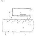
- the schematic diagram of a length or angle measuring system 1 shown in FIG. 1 shows sections of a measuring standard 2 which bears a periodic measuring graduation 3.
- the measuring graduation 3 consists of S poles (source) and D poles (drain) of a series of field-effect transistor components S and D, which are strung together as a periodic measuring graduation 3 in the measuring direction.
- This series of source and drain regions S and D is scanned during relative movements between the material measure 2 and a scanning device 4.
- the scanning takes place by means of a control electrode (gate) G, which is located in the scanning device 4.
- the control electrode G forms an electron-conducting channel and bridges the source and drain regions S and D of the measuring graduation 3 and completes or activates it thus each of the field effect transistor components S and D forming the measuring division 3 to form a field effect transistor SDG.
- the mode of operation of the measuring system 1 is based on the switching of individual transistor components, the source and drain regions S and D of the transistor alternatingly being diffused into silicon periodically as material measure 2, and a semiconductor substrate other than Si is also conceivable.
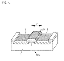
- a single transistor SDG is shown by way of example in FIG. 4, the substrate of the material measure 2 being p-conducting silicon.
- the source and drain regions S and D are heavily n-doped.
- the - movable in the measuring system - single gate electrode G (metal) is electrically separated from the substrate 2 by an insulator I and relatively movable to the measuring graduation 3.
- the area under the gate G between source S and drain D can be depleted or enriched with electrons.
- an electron-conducting channel, the “inversion layer” is formed between source S and drain D, in this case the transistor SDG is operated in saturation.
- the operation of the measuring system is possible not only in the saturation range but also in the amplification range of the transistor SDG, which will be discussed in detail later.
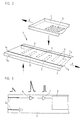
- FIG. 1 A possible, schematic embodiment is shown in FIG. The reference numerals according to FIG. 1 are retained, but the perspective representation is intended to facilitate reference to conventional length or angle measuring devices.
- the scanning unit 4 also consists of silicon, in which one or more gate electrodes G are integrated. It is also possible to lower the gate structure, for example by selective etching processes in silicon.
- the scanning unit 4 and the scale 2 can be guided against each other in contact or at a defined distance.
- moving scanning unit 4 (gate electrode G) and scale 2 at a defined distance depending on the substrate doping and the applied gate voltage, a defined distance must be maintained in order to maintain the electron-conducting channel.
- the body 2 is regarded as a partial section of a material measure, which is already shown in FIGS. 1 and 2. Between two doped regions S and D, which represent two poles of a field effect transistor SDG, a region is placed which forms the gate G of the aforementioned transistor SDG.
- transistors SDG as activatable components for length measurement
- electrical pulses can be processed directly.
- the electrical connections of the active scale surface and further processing electronics on the back of the scale 2 can be produced by conductor tracks 5 recessed in trenches 5a.
- optional components for signal processing amplifier 6, signal multiplication 7) and the read-out unit 8 (eg optical LCD display) can be integrated.
- signal processing amplifier 6, signal multiplication 7
- read-out unit 8 eg optical LCD display
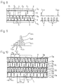
- FIGS. 5 to 10 each show an advantageous embodiment in a highly schematic representation, the description of which now follows.
- the representation in FIGS. 1 and 2 is based on this, so that the two-dimensional representation of the source and drain regions and the control electrode has been dispensed with in favor of the simpler line representation.
- FIG. 5 shows a material measure 2, on the substrate of which two tracks a and b are arranged.
- Track a has alternating source and drain regions S and D in the measuring direction X, each of which extends from a common collecting line 5 S or 5 D perpendicular to the measuring direction X and which form an incremental division as the measuring division 3.
- source and drain regions S and D which form two reference marks R 1 and R 2 , at selected locations - applied in the same way as the measuring graduation 3 on the substrate 2.
- a scanning device 4 which contains a control electrode G, is shown with dashed lines.
- FIG. 6 shows an arrangement similar to that of FIG. 5.
- three reference marks R 1 , R 2 , R 3 are applied to the substrate 2 in the same way.
- R 1 , R 2 and R 3 can be selected.
- only one reference mark, namely R 3 should be activated. This can be done by connecting the reference marks R 1 , R 2 , R 3 accordingly.
- the source bus 5 S is led to the reference mark R 3 , the source connection to the reference marks R 1 and R 2 is interrupted. As a result, they cannot be activated when the control electrode G is run over. This can also be seen in the pulse diagram opposite.
- a reference mark can also be selected by operating different reference marks in different amplification areas during the evaluation. This is illustrated with the aid of FIG. 7 and can be seen in particular from the associated pulse diagram. The different levels of the pulses J R1 and J R2 are caused by operation in different amplification areas. A reference mark can be selected using appropriate threshold switches or the like. The same picture emerges if the different reference marks are operated with different bias voltages of their source and drain regions.
- control electrode G for the measuring graduation 3 two further control electrodes G1 and G2 are provided in the scanning device 4.
- individual reference marks can be targeted R 1 or R 2 can be selected.
- the control voltages, the bias voltages of the source and drain regions, and the amplification regions can be varied as desired, and combinations of these variations are of course also possible.
- the pulse diagram can correspond to the one shown. The changes in position of the pulses that occur due to the spatial offset of the control electrodes G1 and G2 can be used in a targeted manner, but they can also be compensated for by appropriate offset of the reference marks on the substrate.
- FIG. 9 Another very advantageous possibility for evaluating reference marks is illustrated in FIG. 9 using a pulse diagram.
- a reference mark not shown, has a plurality of source and drain regions. This differentiates their structure from that of the previously considered reference marks.
- source and drain regions can be combined in terms of circuitry, but a single source and drain region can also be arranged between or in addition to combined source and drain regions.
- both the combined and the individual source and drain regions can be operated with different bias voltages and / or in different amplification regions.
- Such operation can generate a pulse train as shown in FIG. 9.
- J SD1 means that a pulse is present which has arisen from two combined source and drain regions of a first bias voltage (or a first amplification region).
- the pulse J SD2 has emerged from two combined source and drain regions of a second bias voltage (or a second amplification region).
- the pulse J SD3 is made up of (again two) combined source and drain regions a third bias (or a third gain range) emerged.
- pulses J SD4 , J SD5 and J SD6 which are each obtained at individual source-drain regions, but are operated with different fourth, fifth and sixth bias voltages or corresponding amplification regions.
- the envelope is an asymmetrical curve.
- Their evaluation can advantageously be used to identify the direction from which the reference mark designed in this way was passed.
- Such asymmetrical reference marks can be used particularly advantageously as limit switches.
- FIG. 10 finally shows an exemplary embodiment in which a plurality of tracks a, c, d, e are provided on a substrate 2.
- a, c, d and e there are alternating source and drain regions which are arranged periodically and each form a periodic measurement graduation 3a, 3c, 3d and 3e.
- These measurement divisions 3a, 3c, 3d and 3e are periodic, but each of the measurement graduations 3a, 3c, 3d and 3e has a different division period Pa, Pc, Pd, Pe.
- the technical embodiment corresponds, for example, to four parallel measuring devices according to FIG. 2, and the source and drain busbars are designated accordingly.
- An analogy to the above exemplary embodiments can be readily derived by the person skilled in the art, so that the basic functional principles need not be explained again.
- the measuring system 1 described is based on the fact that an electron-conducting inversion layer is switched on and off in a semiconductor, depending on the local position of the gate electrode G.
- the system described above is independent of optical signals and components. Thus, no "aging" of the measuring system 1 is to be expected over time (degradation of the intensities of laser diodes with long operating times).
- the measuring system 1 described above can be designed as a length measuring system or as an angle measuring system.
- Silicon has excellent mechanical properties, such as scratch resistance.
- the purity of the crystal ensures high reproducibility of the electronic properties of the measuring system.
- HEMT high-electron mobility transistor
Landscapes
- Physics & Mathematics (AREA)
- General Physics & Mathematics (AREA)
- Junction Field-Effect Transistors (AREA)
- Measurement Of Length, Angles, Or The Like Using Electric Or Magnetic Means (AREA)
- Testing Or Measuring Of Semiconductors Or The Like (AREA)
Priority Applications (1)
| Application Number | Priority Date | Filing Date | Title |
|---|---|---|---|
| DE59404747T DE59404747D1 (de) | 1994-07-01 | 1994-07-01 | Längen- oder Winkelmesseinrichtung |
Applications Claiming Priority (1)
| Application Number | Priority Date | Filing Date | Title |
|---|---|---|---|
| EP94110254A EP0693672B1 (de) | 1994-07-01 | 1994-07-01 | Längen- oder Winkelmesseinrichtung |
Related Parent Applications (1)
| Application Number | Title | Priority Date | Filing Date |
|---|---|---|---|
| EP94110254.3 Division | 1994-07-01 |
Publications (3)
| Publication Number | Publication Date |
|---|---|
| EP0730137A2 EP0730137A2 (de) | 1996-09-04 |
| EP0730137A3 EP0730137A3 (OSRAM) | 1996-09-25 |
| EP0730137B1 true EP0730137B1 (de) | 1997-12-03 |
Family
ID=8216075
Family Applications (2)
| Application Number | Title | Priority Date | Filing Date |
|---|---|---|---|
| EP96109083A Expired - Lifetime EP0730137B1 (de) | 1994-07-01 | 1994-07-01 | Längen- oder Winkelmesseinrichtung |
| EP94110254A Expired - Lifetime EP0693672B1 (de) | 1994-07-01 | 1994-07-01 | Längen- oder Winkelmesseinrichtung |
Family Applications After (1)
| Application Number | Title | Priority Date | Filing Date |
|---|---|---|---|
| EP94110254A Expired - Lifetime EP0693672B1 (de) | 1994-07-01 | 1994-07-01 | Längen- oder Winkelmesseinrichtung |
Country Status (2)
| Country | Link |
|---|---|
| EP (2) | EP0730137B1 (OSRAM) |
| DE (2) | DE59401352D1 (OSRAM) |
Families Citing this family (5)
| Publication number | Priority date | Publication date | Assignee | Title |
|---|---|---|---|---|
| GB9522491D0 (en) * | 1995-11-02 | 1996-01-03 | Renishaw Plc | Opto-electronic rotary encoder |
| NL1025523C2 (nl) * | 2004-02-19 | 2005-08-22 | Iku Holding Montfoort Bv | Mechatronisch regelsysteem. |
| DE102009002723A1 (de) | 2009-04-29 | 2010-11-04 | Robert Bosch Gmbh | Messelement |
| DE102015213784B4 (de) * | 2014-08-13 | 2020-07-09 | Robert Bosch Gmbh | Positionsmesssystem mit Empfängerspulen, die über Schaltmittel differentiell zusammenschaltbar sind |
| EP3255375A1 (de) * | 2016-06-10 | 2017-12-13 | CTR Carinthian Tech Research AG | Verfahren und sensor zur kontaktlosen messung einer distanz |
Family Cites Families (7)
| Publication number | Priority date | Publication date | Assignee | Title |
|---|---|---|---|---|
| DE2720869C2 (de) * | 1977-05-10 | 1979-02-08 | Team-Technik Gesellschaft Fuer Entwicklung Und Vertrieb Von Maschinen Und Anglagen Mbh, 7141 Freiberg | Vorrichtung zur direkten und/oder bewerteten Erfassung und Anzeige einer Meßstrecke mittels eines Maßstabes mit Schieber |
| US4767973A (en) * | 1987-07-06 | 1988-08-30 | Sarcos Incorporated | Systems and methods for sensing position and movement |
| DE3914739A1 (de) * | 1989-05-05 | 1990-11-08 | Heidenhain Gmbh Dr Johannes | Inkrementale positionsmesseinrichtung mit referenzmarken |
| US5198740A (en) * | 1989-10-04 | 1993-03-30 | University Of Utah Research Foundation | Sliding contact mechanical/electrical displacement transducer |
| EP0491567A1 (en) * | 1990-12-19 | 1992-06-24 | Honeywell Inc. | Integrated sensor assembly |
| DE4212952C2 (de) * | 1991-08-03 | 1994-06-09 | Heidenhain Gmbh Dr Johannes | Längen- oder Winkelmeßeinrichtung |
| JPH05130618A (ja) * | 1991-11-06 | 1993-05-25 | Hamamatsu Photonics Kk | 赤外線画像認識装置 |
-
1994
- 1994-07-01 DE DE59401352T patent/DE59401352D1/de not_active Expired - Fee Related
- 1994-07-01 EP EP96109083A patent/EP0730137B1/de not_active Expired - Lifetime
- 1994-07-01 EP EP94110254A patent/EP0693672B1/de not_active Expired - Lifetime
-
1995
- 1995-06-22 DE DE19522611A patent/DE19522611A1/de not_active Withdrawn
Also Published As
| Publication number | Publication date |
|---|---|
| EP0730137A3 (OSRAM) | 1996-09-25 |
| DE19522611A1 (de) | 1996-01-04 |
| EP0693672A1 (de) | 1996-01-24 |
| DE59401352D1 (de) | 1997-01-30 |
| EP0730137A2 (de) | 1996-09-04 |
| EP0693672B1 (de) | 1996-12-18 |
Similar Documents
| Publication | Publication Date | Title |
|---|---|---|
| EP1540748B9 (de) | Magnetfeldsensor mit einem hallelement | |
| EP0244577B1 (de) | Integrierbares Hallelement | |
| DE69312619T2 (de) | Magnetischer Positionsgeber | |
| EP0114371B1 (de) | MISFET mit Eingangsverstärker | |
| DE102013213734B4 (de) | Strom-Sense-Transistor mit Einbettung von Sense-Transistorzellen und Verfahren zur Herstellung | |
| EP0202508B1 (de) | Einrichtung mit einem in einer integrierten Schaltung integrierbaren Hallelement | |
| EP2449394A1 (de) | Hall-sensorelement und verfahren zur messung eines magnetfelds | |
| EP1206707A1 (de) | Hall-sensoranordnung zur offset-kompensierten magnetfeldmessung | |
| DE69533134T2 (de) | Leistungsbauteil hoher Dichte in MOS-Technologie | |
| DE19733974C2 (de) | MOSFET-Einrichtung und Verfahren zur Herstellung | |
| DE2804373A1 (de) | Hall-generator | |
| EP0730137B1 (de) | Längen- oder Winkelmesseinrichtung | |
| DE69610775T2 (de) | Geschalteter magnetfeldempfindlicher feldeffekttransistor | |
| DE102014222214A1 (de) | Integrierte Halbleiterschaltung | |
| DE2520608B2 (de) | Halbleiteranordnung zum Digitalisieren eines analogen elektrischen Eingangssignals | |
| DE2103542A1 (de) | Kraftmeßvorrichtung | |
| DE3853657T2 (de) | Magnetoelektrisches Element und Magnetoelektrischer Apparat. | |
| DE2725154C3 (de) | Verfahren zur Herstellung eines zweiphasigen ladungsgekoppelten Halbleiterbauelements | |
| DE3731000A1 (de) | Integrierte halbleiteranordnung | |
| DE102016109971B3 (de) | Spinning-current-verfahren für magfet-sensor | |
| DE19834234A1 (de) | Integrierter Halbleiterchip mit modularen Füllstrukturen | |
| EP0004563A1 (de) | Transversalfilter | |
| DE10223179B4 (de) | Widerstandsbauelement und Verfahren zum Betreiben des Widerstandsbauelements | |
| DE2654316A1 (de) | Halbleitervorrichtung | |
| DE2734366A1 (de) | Komplementaere eingangsstruktur fuer eine ladungsgekoppelte 2-kanal- anordnung |
Legal Events
| Date | Code | Title | Description |
|---|---|---|---|
| PUAI | Public reference made under article 153(3) epc to a published international application that has entered the european phase |
Free format text: ORIGINAL CODE: 0009012 |
|
| PUAL | Search report despatched |
Free format text: ORIGINAL CODE: 0009013 |
|
| AC | Divisional application: reference to earlier application |
Ref document number: 693672 Country of ref document: EP |
|
| AK | Designated contracting states |
Kind code of ref document: A2 Designated state(s): DE FR GB IT |
|
| AK | Designated contracting states |
Kind code of ref document: A3 Designated state(s): DE FR GB IT |
|
| 17P | Request for examination filed |
Effective date: 19960829 |
|
| 17Q | First examination report despatched |
Effective date: 19961119 |
|
| GRAG | Despatch of communication of intention to grant |
Free format text: ORIGINAL CODE: EPIDOS AGRA |
|
| GRAG | Despatch of communication of intention to grant |
Free format text: ORIGINAL CODE: EPIDOS AGRA |
|
| GRAH | Despatch of communication of intention to grant a patent |
Free format text: ORIGINAL CODE: EPIDOS IGRA |
|
| GRAH | Despatch of communication of intention to grant a patent |
Free format text: ORIGINAL CODE: EPIDOS IGRA |
|
| GRAA | (expected) grant |
Free format text: ORIGINAL CODE: 0009210 |
|
| AC | Divisional application: reference to earlier application |
Ref document number: 693672 Country of ref document: EP |
|
| AK | Designated contracting states |
Kind code of ref document: B1 Designated state(s): DE FR GB IT |
|
| ET | Fr: translation filed | ||
| GBT | Gb: translation of ep patent filed (gb section 77(6)(a)/1977) |
Effective date: 19971203 |
|
| REF | Corresponds to: |
Ref document number: 59404747 Country of ref document: DE Date of ref document: 19980115 |
|
| PLBE | No opposition filed within time limit |
Free format text: ORIGINAL CODE: 0009261 |
|
| STAA | Information on the status of an ep patent application or granted ep patent |
Free format text: STATUS: NO OPPOSITION FILED WITHIN TIME LIMIT |
|
| 26N | No opposition filed | ||
| REG | Reference to a national code |
Ref country code: GB Ref legal event code: IF02 |
|
| PGFP | Annual fee paid to national office [announced via postgrant information from national office to epo] |
Ref country code: GB Payment date: 20020628 Year of fee payment: 9 |
|
| PGFP | Annual fee paid to national office [announced via postgrant information from national office to epo] |
Ref country code: FR Payment date: 20020711 Year of fee payment: 9 |
|
| PG25 | Lapsed in a contracting state [announced via postgrant information from national office to epo] |
Ref country code: GB Free format text: LAPSE BECAUSE OF NON-PAYMENT OF DUE FEES Effective date: 20030701 |
|
| GBPC | Gb: european patent ceased through non-payment of renewal fee |
Effective date: 20030701 |
|
| PG25 | Lapsed in a contracting state [announced via postgrant information from national office to epo] |
Ref country code: FR Free format text: LAPSE BECAUSE OF NON-PAYMENT OF DUE FEES Effective date: 20040331 |
|
| REG | Reference to a national code |
Ref country code: FR Ref legal event code: ST |
|
| PG25 | Lapsed in a contracting state [announced via postgrant information from national office to epo] |
Ref country code: IT Free format text: LAPSE BECAUSE OF NON-PAYMENT OF DUE FEES;WARNING: LAPSES OF ITALIAN PATENTS WITH EFFECTIVE DATE BEFORE 2007 MAY HAVE OCCURRED AT ANY TIME BEFORE 2007. THE CORRECT EFFECTIVE DATE MAY BE DIFFERENT FROM THE ONE RECORDED. Effective date: 20050701 |
|
| PGFP | Annual fee paid to national office [announced via postgrant information from national office to epo] |
Ref country code: DE Payment date: 20050714 Year of fee payment: 12 |
|
| PG25 | Lapsed in a contracting state [announced via postgrant information from national office to epo] |
Ref country code: DE Free format text: LAPSE BECAUSE OF NON-PAYMENT OF DUE FEES Effective date: 20070201 |