EP0724299A2 - Vorrichtung mit Photodetektor auf Siliziumbasis - Google Patents
Vorrichtung mit Photodetektor auf Siliziumbasis Download PDFInfo
- Publication number
- EP0724299A2 EP0724299A2 EP96300306A EP96300306A EP0724299A2 EP 0724299 A2 EP0724299 A2 EP 0724299A2 EP 96300306 A EP96300306 A EP 96300306A EP 96300306 A EP96300306 A EP 96300306A EP 0724299 A2 EP0724299 A2 EP 0724299A2
- Authority
- EP
- European Patent Office
- Prior art keywords
- layer
- crystalline
- radiation
- contacts
- photodetector
- Prior art date
- Legal status (The legal status is an assumption and is not a legal conclusion. Google has not performed a legal analysis and makes no representation as to the accuracy of the status listed.)
- Granted
Links
Images
Classifications
-
- H—ELECTRICITY
- H10—SEMICONDUCTOR DEVICES; ELECTRIC SOLID-STATE DEVICES NOT OTHERWISE PROVIDED FOR
- H10F—INORGANIC SEMICONDUCTOR DEVICES SENSITIVE TO INFRARED RADIATION, LIGHT, ELECTROMAGNETIC RADIATION OF SHORTER WAVELENGTH OR CORPUSCULAR RADIATION
- H10F77/00—Constructional details of devices covered by this subclass
- H10F77/70—Surface textures, e.g. pyramid structures
- H10F77/703—Surface textures, e.g. pyramid structures of the semiconductor bodies, e.g. textured active layers
-
- Y—GENERAL TAGGING OF NEW TECHNOLOGICAL DEVELOPMENTS; GENERAL TAGGING OF CROSS-SECTIONAL TECHNOLOGIES SPANNING OVER SEVERAL SECTIONS OF THE IPC; TECHNICAL SUBJECTS COVERED BY FORMER USPC CROSS-REFERENCE ART COLLECTIONS [XRACs] AND DIGESTS
- Y02—TECHNOLOGIES OR APPLICATIONS FOR MITIGATION OR ADAPTATION AGAINST CLIMATE CHANGE
- Y02E—REDUCTION OF GREENHOUSE GAS [GHG] EMISSIONS, RELATED TO ENERGY GENERATION, TRANSMISSION OR DISTRIBUTION
- Y02E10/00—Energy generation through renewable energy sources
- Y02E10/50—Photovoltaic [PV] energy
Definitions
- This invention pertains to the field of semiconductor photodetectors, and to articles that comprise such photodetectors, e.g., optical interconnects.
- Si-based photodetector/receiver combination would be substantially less expensive than the prior art GaAs-based combination.
- more electronic functionality could typically be built into a Si-based combination than into a GaAs-based combination, due to the far greater maturity of Si technology.
- the long absorption length of electromagnetic radiation in crystalline Si produces two problems.
- a Si-based photodetector e.g., a metal-semiconductor-metal detector
- the quantum efficiency ⁇ of the detector will be quite low.
- the photocarrier generated below the depletion region will be collected by diffusion rather than field induced drift, resulting in a slow detector.
- prior art Si-based photodetectors typically can not simultaneously have high (e.g., ⁇ 20%) quantum efficiency and high (e.g., ⁇ 1 Gb/s) speed.
- FWHM full width at half maximum
- a textured surface we mean herein a surface that exhibits surface features, typically substantially randomly distributed features, so as to (randomly or pseudo-randomly) scatter radiation of a predetermined wavelength ⁇ incident on the surface.
- statistical measures of the surface features including an average feature size.
- the average feature size typically can be determined from, e.g., a scanning electron microscope (SEM) micrograph of the surface.
- the invention is defined by the claims.
- the photodetector comprises a crystalline Si (silicon) layer disposed on a dielectric material, and spaced apart first and second contacts to the Si layer.
- the article also comprises a voltage source for applying a bias voltage between said first and second contacts, and apparatus (typically intergrated receiver circuitry) that is responsive to the current between said first and second contacts.
- the Si layer has a major surface, and the current is responsive to electromagnetic radiation of wavelength ⁇ that is incident on the major surface and transmitted therethrough.
- the thickness t of the crystalline Si layer is less (typically substantially less) than the absorption length ⁇ -1 in crystalline Si of the radiation of wavelength ⁇
- the dielectric material has a refractive index that is less than the refractive index of crystalline Si at ⁇ , and at least a portion of the major surface is textured such that the propagation direction of radiation of wavelength ⁇ that is incident on the textured surface is substantially randomized.
- the photodetector is a MSM photodetector, and the first and second contacts are disposed on the major surface of the Si layer.
- the photodetector is a p-n junction device, with a first portion of the Si layer being n-type and a second portion being p-type, with the first and second contacts contacting the first and second portions, respectively.
- the substantially randomized radiation that results from transmission through the textured surface is substantially confined in the Si layer, resulting in an effective path length in the Si layer that can be substantially longer than the thickness of the Si layer. Consequently, detectors according to the invention can at the same time have relatively high (e.g., ⁇ 20%) quantum efficiency and speed (e.g., ⁇ 1Gb/s).
- U.S. Patent Application Serial No. 08/336,946, filed November 10, 1994 by B.F. Levine et al. discloses a quantum well infrared photodetector (QWIP) that has a surface that is patterned to pseudo-randomly reflect radiation. See also G. Sarusi et al., Applied Physics Letters , Vol. 64(8), p. 960, February 1994, which discloses such QWIPs. Si-based solar cells with textured surface are also known. See, for instance, T. Tiedje et al., IEEE Transactions on Electron Devices , Vol. ED 31(5), p. 711.
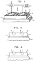
- FIG. 1 A portion of the exemplary photodetector is schematically depicted in FIG. 1, wherein numerals 10-12 refer, respectively, to a substrate (typically Si), a dielectric (typically SiO 2 ) layer, and a high quality crystalline Si (active) layer.
- Si-on-insulator (SOI) wafers of the type used to make the device shown in FIG. 1 are well known and are commercially available.
- the buried SiO 2 layer is exemplarily about 0.4-1 ⁇ m thick, and the thickness t of layer 12 is selected to be substantially less than the relevant absorption length ⁇ -1 in Si, typically ⁇ 0.5 ⁇ -1 .
- t is selected to be approximately equal to the product of hole drift velocity v h in the lowest electric field region and the maximum response time ⁇ of the device.
- the former typically is about 10 6 cm/s, and for 1Gb/s operation of the detector ⁇ should be ⁇ 300ps.
- the thickness of layer 12 thus exemplarily is selected to be about 3 ⁇ m, typically in the range 1.5-5 ⁇ m.
- the doping of the Si active layer is advantageously selected such that the layer is substantially depleted at anticipated bias voltages, e.g., at CMOS bias voltage levels of 3.5 - 5 V.
- the active layer doping is ⁇ 10 16 cm -3 , exemplarily about 10 15 cm -3 p-type.
- a textured Si surface suitable for devices according to the invention can be produced, for instance, by plasma etching.
- a suitable textured surface results when about 1 ⁇ m of layer 12 is removed, using a helicon high density plasma source, with the highly Si/SiO 2 selective gas mixture of 69% HBr, 22% He, 5.5% O 2 and 3.5% SF 6 at the pressure of 5 mTorr, a RF source power of 2500W and a chuck bias of 50V.
- the average feature size is in the range 0.2 ⁇ /n to 5 ⁇ /n, where n is the refractive index of crystalline Si for radiation of (vacuum) wavelength ⁇ .
- n is the refractive index of crystalline Si for radiation of (vacuum) wavelength ⁇ .
- the average feature size is ( ⁇ /2n) ⁇ 50%.
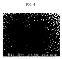
- the textured surface had, in SEM micrographs, a "hill and dale” appearance, with substantially rounded “hills", as can be seen from FIG. 4.
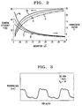
- FIG. 2 shows results of such a calculation, for 1 ⁇ m wide interdigitated metal electrodes on the surface, with 4 ⁇ m spacing between the electrodes.
- Reference numerals 14 and 15 in FIG. 1 designate the electrodes, and numerals 16 refer to an appropriate bias voltage source and receiver, respectively. Voltage source and receiver can be conventional.
- FIG. 1 of the previously cited C.-C. Wang paper shows an exemplary set of interdigitated electrodes in plan view, and the previously cited Yamanaka paper (incorporated herein by reference) shows, inter alia, receiver circuitry and an integrated array of photodetectors and receivers.
- FIG. 2 shows that quite large values of ⁇ can be attained even for rather small values of ⁇ t.
- the figure also shows that ⁇ also depends on the composition of the electrodes, with Ag yielding the highest values and Ti the lowest, with Al being intermediate.
- a Ti layer On the above described textured surface of the exemplary wafer was deposited a Ti layer, which was then patterned by conventional means into 100 ⁇ m square interdigitated MSM patterns with 1.6 ⁇ m finger linewidths and 4.4 ⁇ m finger spacings. Ti was chosen for the metal contacts to provide a stringent test, since it has relatively low reflectivity. Other contact metals can be used.
- the same electrode patterns were also formed on an untextured portion of the same wafer, to provide side by side comparison.
- the speed of the above described exemplary SMS detector according to the invention was tested with a 1 Gb/s square wave laser signal. Exemplary results are shown in FIG. 3. The rise and fall times are about 200 ps. The bumps on the trace are unrelated to detector performance.
- FIGs. 5 and 6 schematically depict a portion of a p-i-n-type photodetector and of a photoconductor-type photodetector.
- numerals 51 and 52 refer to p- and n-doped regions, whereas in the latter regions 61 are of the same conductivity type, exemplarily p-type.
- the above discussed selection criteria for, e.g., thickness and doping of the active layer 12, and average feature size of textured surface 13 typically apply to all embodiments of the invention.
- Contacts are conventional and may be ohmic or non-ohmic.
- the invention can be embodied in an article that comprises a discrete photodetector according to the invention, the invention is most advantageously embodied in an article that comprises an integrated array of photodetectors and associated circuitry.
- integrated arrays can be used, for instance, in optical interconnect apparatus or optical links. See, for instance, FIG. 2 of the previously referenced Yamanaka paper.
- a detector according to the invention, with integrated associated circuitry can be advantageously used, for instance, on subscriber premises for fiber-to-the-home broadband communication systems. For all these applications the potentially relatively low cost and high functionality of integrated Si-based photodetector/circuitry combinations will be of advantage.
Landscapes
- Light Receiving Elements (AREA)
Applications Claiming Priority (2)
| Application Number | Priority Date | Filing Date | Title |
|---|---|---|---|
| US379422 | 1982-05-18 | ||
| US08/379,422 US5589704A (en) | 1995-01-27 | 1995-01-27 | Article comprising a Si-based photodetector |
Publications (3)
| Publication Number | Publication Date |
|---|---|
| EP0724299A2 true EP0724299A2 (de) | 1996-07-31 |
| EP0724299A3 EP0724299A3 (de) | 1997-04-02 |
| EP0724299B1 EP0724299B1 (de) | 2001-11-21 |
Family
ID=23497208
Family Applications (1)
| Application Number | Title | Priority Date | Filing Date |
|---|---|---|---|
| EP96300306A Expired - Lifetime EP0724299B1 (de) | 1995-01-27 | 1996-01-16 | Vorrichtung mit Photodetektor auf Siliziumbasis |
Country Status (4)
| Country | Link |
|---|---|
| US (1) | US5589704A (de) |
| EP (1) | EP0724299B1 (de) |
| JP (1) | JPH08242015A (de) |
| DE (1) | DE69617064T2 (de) |
Cited By (3)
| Publication number | Priority date | Publication date | Assignee | Title |
|---|---|---|---|---|
| WO2000057487A1 (fr) * | 1999-03-22 | 2000-09-28 | Onera (Office National D'etudes Et De Recherches Aerospatiales) | Dispositif opto-electronique premuni contre les detections par un faisceau lumineux collimate |
| EP1845562A1 (de) * | 2005-11-10 | 2007-10-17 | Tatung Company | Antireflexsubstrat und Herstellungsverfahren dafür |
| EP2560215A4 (de) * | 2010-04-14 | 2014-04-09 | Hamamatsu Photonics Kk | Halbleiter-lichterkennungselement |
Families Citing this family (27)
| Publication number | Priority date | Publication date | Assignee | Title |
|---|---|---|---|---|
| TW415103B (en) * | 1998-03-02 | 2000-12-11 | Ibm | Si/SiGe optoelectronic integrated circuits |
| CA2365499C (en) | 2000-12-26 | 2011-02-15 | National Research Council Of Canada | High speed and high efficiency si-based photodetectors using waveguides formed with silicides for near ir applications |
| US7442629B2 (en) | 2004-09-24 | 2008-10-28 | President & Fellows Of Harvard College | Femtosecond laser-induced formation of submicrometer spikes on a semiconductor substrate |
| US7057256B2 (en) | 2001-05-25 | 2006-06-06 | President & Fellows Of Harvard College | Silicon-based visible and near-infrared optoelectric devices |
| KR100678291B1 (ko) * | 2004-11-11 | 2007-02-02 | 삼성전자주식회사 | 나노입자를 이용한 수광소자 |
| US8329046B2 (en) * | 2009-02-05 | 2012-12-11 | Asia Union Electronic Chemical Corporation | Methods for damage etch and texturing of silicon single crystal substrates |
| JP5185206B2 (ja) | 2009-02-24 | 2013-04-17 | 浜松ホトニクス株式会社 | 半導体光検出素子 |
| JP5185205B2 (ja) * | 2009-02-24 | 2013-04-17 | 浜松ホトニクス株式会社 | 半導体光検出素子 |
| JP5185207B2 (ja) | 2009-02-24 | 2013-04-17 | 浜松ホトニクス株式会社 | フォトダイオードアレイ |
| JP5185208B2 (ja) | 2009-02-24 | 2013-04-17 | 浜松ホトニクス株式会社 | フォトダイオード及びフォトダイオードアレイ |
| JP2010283223A (ja) * | 2009-06-05 | 2010-12-16 | Hamamatsu Photonics Kk | 半導体光検出素子及び半導体光検出素子の製造方法 |
| US9673243B2 (en) | 2009-09-17 | 2017-06-06 | Sionyx, Llc | Photosensitive imaging devices and associated methods |
| US9911781B2 (en) | 2009-09-17 | 2018-03-06 | Sionyx, Llc | Photosensitive imaging devices and associated methods |
| JP2011066316A (ja) * | 2009-09-18 | 2011-03-31 | Asahi Kasei Electronics Co Ltd | 光センサ |
| JP5427531B2 (ja) * | 2009-09-29 | 2014-02-26 | 三菱重工業株式会社 | 光検出素子、光検出装置及び赤外線検出素子、赤外線検出装置 |
| US8120027B2 (en) * | 2009-12-10 | 2012-02-21 | Leonard Forbes | Backside nanoscale texturing to improve IR response of silicon solar cells and photodetectors |
| US8212250B2 (en) | 2009-12-10 | 2012-07-03 | Leonard Forbes | Backside texturing by cusps to improve IR response of silicon solar cells and photodetectors |
| JP5616099B2 (ja) * | 2010-04-01 | 2014-10-29 | 浜松ホトニクス株式会社 | 距離センサ及び距離画像センサ |
| US8692198B2 (en) | 2010-04-21 | 2014-04-08 | Sionyx, Inc. | Photosensitive imaging devices and associated methods |
| EP2583312A2 (de) | 2010-06-18 | 2013-04-24 | Sionyx, Inc. | Lichtempfindliche hochgeschwindigkeitsvorrichtungen und verfahren dafür |
| US9496308B2 (en) | 2011-06-09 | 2016-11-15 | Sionyx, Llc | Process module for increasing the response of backside illuminated photosensitive imagers and associated methods |
| EP2732402A2 (de) | 2011-07-13 | 2014-05-21 | Sionyx, Inc. | Biometrische bildgebungsvorrichtungen und entsprechende verfahren |
| US9064764B2 (en) | 2012-03-22 | 2015-06-23 | Sionyx, Inc. | Pixel isolation elements, devices, and associated methods |
| JP6466346B2 (ja) | 2013-02-15 | 2019-02-06 | サイオニクス、エルエルシー | アンチブルーミング特性を有するハイダイナミックレンジcmos画像センサおよび関連づけられた方法 |
| US9939251B2 (en) | 2013-03-15 | 2018-04-10 | Sionyx, Llc | Three dimensional imaging utilizing stacked imager devices and associated methods |
| US9209345B2 (en) | 2013-06-29 | 2015-12-08 | Sionyx, Inc. | Shallow trench textured regions and associated methods |
| US10879407B2 (en) | 2016-09-27 | 2020-12-29 | Nec Corporation | Optical sensor and method for forming same |
Family Cites Families (2)
| Publication number | Priority date | Publication date | Assignee | Title |
|---|---|---|---|---|
| JPS60140752A (ja) * | 1983-12-28 | 1985-07-25 | Olympus Optical Co Ltd | 半導体光電変換装置 |
| US4989972A (en) * | 1989-05-01 | 1991-02-05 | Hewlett-Packard Company | Low reflectivity surface relief gratings for photodetectors |
-
1995
- 1995-01-27 US US08/379,422 patent/US5589704A/en not_active Expired - Lifetime
-
1996
- 1996-01-16 DE DE69617064T patent/DE69617064T2/de not_active Expired - Fee Related
- 1996-01-16 EP EP96300306A patent/EP0724299B1/de not_active Expired - Lifetime
- 1996-01-26 JP JP8011365A patent/JPH08242015A/ja active Pending
Cited By (6)
| Publication number | Priority date | Publication date | Assignee | Title |
|---|---|---|---|---|
| WO2000057487A1 (fr) * | 1999-03-22 | 2000-09-28 | Onera (Office National D'etudes Et De Recherches Aerospatiales) | Dispositif opto-electronique premuni contre les detections par un faisceau lumineux collimate |
| FR2791473A1 (fr) * | 1999-03-22 | 2000-09-29 | Onera (Off Nat Aerospatiale) | Dispositif opto-electronique premuni contre les detections par un faisceau lumineux collimate. |
| EP1845562A1 (de) * | 2005-11-10 | 2007-10-17 | Tatung Company | Antireflexsubstrat und Herstellungsverfahren dafür |
| US7524773B2 (en) | 2005-11-10 | 2009-04-28 | Tatung Company | Anti-reflective substrate and the manufacturing method thereof |
| EP2560215A4 (de) * | 2010-04-14 | 2014-04-09 | Hamamatsu Photonics Kk | Halbleiter-lichterkennungselement |
| US9293499B2 (en) | 2010-04-14 | 2016-03-22 | Hamamatsu Photonics K.K. | Semiconductor light detecting element having silicon substrate and conductor |
Also Published As
| Publication number | Publication date |
|---|---|
| US5589704A (en) | 1996-12-31 |
| EP0724299A3 (de) | 1997-04-02 |
| JPH08242015A (ja) | 1996-09-17 |
| DE69617064T2 (de) | 2002-07-18 |
| EP0724299B1 (de) | 2001-11-21 |
| DE69617064D1 (de) | 2002-01-03 |
Similar Documents
| Publication | Publication Date | Title |
|---|---|---|
| EP0724299B1 (de) | Vorrichtung mit Photodetektor auf Siliziumbasis | |
| US5525828A (en) | High speed silicon-based lateral junction photodetectors having recessed electrodes and thick oxide to reduce fringing fields | |
| US7525170B2 (en) | Pillar P-i-n semiconductor diodes | |
| EP0485115B1 (de) | Herstellungsverfahren für eine Opto-elektronische Strahlungsdetektormatrix | |
| TWI577033B (zh) | 具有加強電磁輻射偵測之裝置與相關方法 | |
| US5100478A (en) | Solar cell | |
| US6593636B1 (en) | High speed silicon photodiodes and method of manufacture | |
| EP1063708B1 (de) | Photoleitfähiger Schalter mit verbesserter Halbleiterstruktur | |
| EP1995793A1 (de) | Lichtdiode, verfahren zur herstellung einer derartigen lichtdiode, optische kommunikationsvorrichtung und optisches verbindungsmodul | |
| EP1627454A2 (de) | Auf verunreinigungen basierende wellenleiterdetektoren | |
| US20190019903A1 (en) | SILICON WAVEGUIDE INTEGRATED WITH SILICON-GERMANIUM (Si-Ge) AVALANCHE PHOTODIODE DETECTOR | |
| US12132131B2 (en) | Backside illuminated avalanche photodiode and manufacturing method thereof | |
| WO2021154603A1 (en) | Single photon avalanche diode device | |
| EP1204148A2 (de) | Verbesserter flacher Photodetektor mit einem Resonanzhohlraum | |
| US8247881B2 (en) | Photodiodes with surface plasmon couplers | |
| Schinke et al. | Photodetectors | |
| KR100459894B1 (ko) | 실리콘 수광소자 | |
| KR102290467B1 (ko) | 태양 전지 및 이의 제조 방법 | |
| KR100709645B1 (ko) | 방사 경화된 가시성 p-i-n 검출기 | |
| Vernon et al. | High performance porous silicon solar cell development | |
| EP3886185A1 (de) | Fotovoltaische vorrichtung und verfahren zur herstellung davon | |
| CN117712201B (zh) | 一种硅基高饱和探测器及其制备方法 | |
| KR100654014B1 (ko) | 대구경 수광부를 위한 전극구조를 구비한 포토 다이오드 | |
| US8829418B2 (en) | Photodiode comprising polarizer | |
| CN119497434A (zh) | 一种背入射式雪崩光电探测器及其制备方法 |
Legal Events
| Date | Code | Title | Description |
|---|---|---|---|
| PUAI | Public reference made under article 153(3) epc to a published international application that has entered the european phase |
Free format text: ORIGINAL CODE: 0009012 |
|
| AK | Designated contracting states |
Kind code of ref document: A2 Designated state(s): DE FR GB |
|
| PUAL | Search report despatched |
Free format text: ORIGINAL CODE: 0009013 |
|
| AK | Designated contracting states |
Kind code of ref document: A3 Designated state(s): DE FR GB |
|
| 17P | Request for examination filed |
Effective date: 19970918 |
|
| GRAG | Despatch of communication of intention to grant |
Free format text: ORIGINAL CODE: EPIDOS AGRA |
|
| 17Q | First examination report despatched |
Effective date: 20010531 |
|
| GRAG | Despatch of communication of intention to grant |
Free format text: ORIGINAL CODE: EPIDOS AGRA |
|
| GRAH | Despatch of communication of intention to grant a patent |
Free format text: ORIGINAL CODE: EPIDOS IGRA |
|
| GRAH | Despatch of communication of intention to grant a patent |
Free format text: ORIGINAL CODE: EPIDOS IGRA |
|
| GRAA | (expected) grant |
Free format text: ORIGINAL CODE: 0009210 |
|
| AK | Designated contracting states |
Kind code of ref document: B1 Designated state(s): DE FR GB |
|
| REG | Reference to a national code |
Ref country code: GB Ref legal event code: IF02 |
|
| REF | Corresponds to: |
Ref document number: 69617064 Country of ref document: DE Date of ref document: 20020103 |
|
| PG25 | Lapsed in a contracting state [announced via postgrant information from national office to epo] |
Ref country code: GB Free format text: LAPSE BECAUSE OF NON-PAYMENT OF DUE FEES Effective date: 20020221 |
|
| ET | Fr: translation filed | ||
| PG25 | Lapsed in a contracting state [announced via postgrant information from national office to epo] |
Ref country code: DE Free format text: LAPSE BECAUSE OF NON-PAYMENT OF DUE FEES Effective date: 20020821 |
|
| PLBE | No opposition filed within time limit |
Free format text: ORIGINAL CODE: 0009261 |
|
| STAA | Information on the status of an ep patent application or granted ep patent |
Free format text: STATUS: NO OPPOSITION FILED WITHIN TIME LIMIT |
|
| PG25 | Lapsed in a contracting state [announced via postgrant information from national office to epo] |
Ref country code: FR Free format text: LAPSE BECAUSE OF NON-PAYMENT OF DUE FEES Effective date: 20020930 |
|
| GBPC | Gb: european patent ceased through non-payment of renewal fee |
Effective date: 20020221 |
|
| REG | Reference to a national code |
Ref country code: FR Ref legal event code: ST |
|
| 26N | No opposition filed | ||
| PG25 | Lapsed in a contracting state [announced via postgrant information from national office to epo] |
Ref country code: DE Free format text: LAPSE BECAUSE OF NON-PAYMENT OF DUE FEES Effective date: 20020131 |