EP0721624B1 - Data reduction in a system for analyzing geometric databases - Google Patents
Data reduction in a system for analyzing geometric databases Download PDFInfo
- Publication number
- EP0721624B1 EP0721624B1 EP94929263A EP94929263A EP0721624B1 EP 0721624 B1 EP0721624 B1 EP 0721624B1 EP 94929263 A EP94929263 A EP 94929263A EP 94929263 A EP94929263 A EP 94929263A EP 0721624 B1 EP0721624 B1 EP 0721624B1
- Authority
- EP
- European Patent Office
- Prior art keywords
- group
- shape
- model
- models
- result
- Prior art date
- Legal status (The legal status is an assumption and is not a legal conclusion. Google has not performed a legal analysis and makes no representation as to the accuracy of the status listed.)
- Expired - Lifetime
Links
Images


Classifications
-
- G—PHYSICS
- G06—COMPUTING OR CALCULATING; COUNTING
- G06F—ELECTRIC DIGITAL DATA PROCESSING
- G06F30/00—Computer-aided design [CAD]
- G06F30/30—Circuit design
- G06F30/39—Circuit design at the physical level
- G06F30/398—Design verification or optimisation, e.g. using design rule check [DRC], layout versus schematics [LVS] or finite element methods [FEM]
Definitions
- This invention relates to computer software and systems used in the design of electronic components and more particularly to a database structure contained within an integrated circuit analyzing computer which reduces the amount of storage memory required to contain database analysis results.
- An integral step in the design and production of integrated circuits involves the computer analysis of the Integrated Circuit (IC) design to verify that each of the geometrical design rules required for effective fabrication of the components is satisfied. These design rules include such parameters as the minimum feature size and the minimum distance between components. Analysis of these circuits has become increasingly difficult over the past decade as the number of electronic devices included on a single integrated circuit is counted in the millions. It is not uncommon for analysis of a complex integrated circuit to take many hours of computation time and require hundreds or thousands of megabytes of storage. Much effort in the past has been devoted to finding ways of performing this analysis more efficiently.
- IC Integrated Circuit
- a system and method for reducing the size of the data set generated from the analysis of layout data used in the design and fabrication of integrated circuits.
- the embodiments of the invention generally involve the generation and use of a specialized register structure for storing analysis results.
- a results register is configured to compress design rule analysis results into fields containing in-group results and override results for each graph entry of the IC database examined.
- In-group results are analysis results which are derived only from the shapes found within the group type being analyzed.
- the results register stores only shape information identifying the type and geometrical placement of the shapes.
- the structure of the present invention is implemented on a general purpose computer, such as a Sun workstation, manufactured by Sun Microsystems, Inc., Mountain View, California.
- the computer uses a Central Processing Unit (CPU) and one or more high speed internal memories which contain program instruction steps and provide storage for the database of the present invention.
- External disk storage is also used to contain original Circuit Data Base (CDB) data relating to the mask layout of the integrated circuit design being analyzed, and to store the Verification Data Base (VDB), which is actually used by the CPU in performing design analysis.
- CDB Circuit Data Base
- VDB Verification Data Base
- a cell reference graph is created in which hierarchical relationships between the various cells are identified. This reference graph identifies a top cell and the hierarchical ordering of lower level cells contained within the IC layout. All cells in the IC layout are identified in a group model register.
- a group model is a collection of pointers to geometries in the shape model register and to other group models in the group model register. The lowest level cell components are called shapes
- the results register is implemented as a memory storage space connected to the CPU, and is used by the CPU to store design analysis results generated during IC layout processing.
- the results register preferably contains analysis results in the form of In-group results and override results.
- the override results contains address pointers to shape model library entries which represent shapes changed by the design analysis.
- FIG. 1 a system 11 is shown for analyzing Integrated Circuit (IC) designs.
- This figure of the high level architecture of the present system 11 shows a conventional general purpose computer 13, having a Central Processing Unit 15 attached via data bus 21 to program memory 17, internal memory 18, Verification Data Base (VDB) memory 19, and an external storage disk 23.
- IC designs generally consist of various lithographic mask layers which are used to produce etched regions of electronic activity within a substrate of crystalline semiconductor material. Each mask layer contains a plurality of geometric shapes for producing specific etched regions. Analysis of these mask layers is performed by examining coordinate representations of these shapes using system 11.
- the coordinate data is produced using a conventional digitizing or layout tool and stored in a format of listed numerical data, herein referred to as the Circuit Data Base (CDB) 22.
- This database is preferably arranged by cells, each cell representing a given area of the final design, and each comprised of references to shapes and other lower level cells.
- the shapes are represented as delimited strings of vertex coordinate points.
- the CDB 22 is conventionally stored in system 11 on an external storage medium such as a disk 23. Since it is not uncommon for the circuit under analysis to contain millions of devices, the complexity of CDB 22 has traditionally made external storage the only practical means for containing this layout data (the strings of coordinates) during processing.
- VDB 19 contains several major components: shape model register 27, group model register 31, reference graph register 24, results register 28, and rain relationship register 26.
- the shape model register 27 contains a library of all shapes used by the IC layout. Each shape used in the IC layout is listed only once in the shape model register 27. In this way, tremendous compression of the IC layout can be achieved, particularly in integrated circuits using large numbers of replicated cells, such as memories.
- the shapes are preferably listed in sequence according to frequency of instantiation in the cells of the CDB 22.
- Each shape model stored within shape model register 27 contains coordinate information identifying vertices of the specific shapes used in the IC layout.
- Shape model register 27 is shown as a table consisting of a column of shape (model) types 34 and shape (model) information 32.
- Each shape type 34 shown in the memory map of FIG. 3 represents a distinct location in internal memory 18.
- Associated with each shape type 34, is a sequential listing of shape information 32. Only one instance of each shape of the integrated circuit layout is contained within the shape model register 27.
- the VDB 19 also contains a group model register 31 for storing a library of group models.
- a group model represents an individual cell within the IC layout. Only one group model is used to represent a cell, regardless of the number of times that cell is referenced in the layout.
- Each group model 31 contains references to: (1) at least two shapes, (2) one or more other group models, or (3) at least one shape and one other group model.
- Each shape or group model reference is represented by a model identifier, a stamping point, and an orientation.
- the model identifier defines the shape or group as an existing shape model, or as an existing group model.
- the stamping point identifies the location of the model (whether a shape or group model) with respect to an absolute location within the cell that references that model.
- a cell that references a model is referred to as that model's "parent.”
- the orientation defines the physical rotation of the model (shape or group) within the model's parent, and with respect to the stamping point of the model. For example, orientation "1" identifies a 90 degree clockwise orientation, orientation "2" indicates that the model is flipped 180 degrees horizontally with respect to the stamping point, and so on.
- the memory map of the group model register 31 is shown illustrating the arrangement of groups within internal memory 18 (FIG. 1).
- the memory map of the group model register 31 consists of two columns.
- the first column is a list of group types 38 where each type listing is contained within a discrete location in internal memory 18.
- Each entry of group information 40 contains a reference to: (1) at least two shape models, (2) one or more other group models, or (3) at least one shape model and one other group model, as well as a reference to design analysis results for the corresponding group.
- FIG. 5 a reference graph 25 is shown, representing in graphical form, the contents of reference graph register 24 (from FIG. 2).
- the reference graph is a data table conventionally used for identifying and organizing the hierarchical relationships between various cells in a layout design.
- One group model in the VDB 19 corresponds to each cell in the graph.
- FIG. 5 shows a simple reference graph 25 including a top cell 57, which is defined to be at Level ⁇ . Internal to the description of the top cell 57 are references to a number of child cells including child 1 through child N. Each of these child cells referenced by top cell 57 are defined to be in Level 1. Similarly, each Level 1 child may reference additional children, creating a layer of Level 2 children.
- each path is also indexed with a data notation which identifies the number of times each child cell is referenced.
- a path 59 is indexed with notation n 1 , where n 1 represents the number of times that child 1 is referenced by its parent cell (top cell 57).
- the path 58 from top cell 57 to child N is indexed as n N indicating that child N is referenced by top cell 57, n N number of times.
- each cell of the layout is accordingly assigned a hierarchical position in VDB 19. Since any cell may occur more than once in an IC layout, the same cell may occur at multiple locations in the reference graph 25. Following one path, a specific cell may be encountered at Level 2, while going down another path, the same cell might be encountered at Level 5.
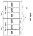
- FIG. 6(a) a memory map of the results register 28 (from FIG. 2) is shown.
- the memory map of results register 28 contains one "row" for each group model type 33 in the design, and shows a series of column sets of rule processing results 42 (separately, 42(a), and 42(b)), one for each verification rule processed. This series of column sets continues to produce N number of column sets representing N number of design rules analyzed.
- the first column of rule processing results shown in column set 42(a) is the "In-group results" 35 which are derived only from the shapes within that group type.
- Column 37 contains override results for each group type 33.
- the override results 37 are produced when the spatial relationship between shapes in that group type 33 and shapes in that group type's lower level cell references is such that the lower level results are invalidated.
- An example of an invalid lower level result would be one in which a spacing violation is obviated by the placement of a shape in a higher-level cell overlapping the area of those shapes which violate the spacing requirement.
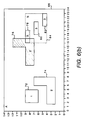
- FIG. 6(b) shows an example of a group model A represented in geometric form.
- the group model A contains both shape models (72, 74, and 76) and another group model, B.
- a bounding box is the smallest rectangle which circumscribes the area of one or more polygons and/or bounding boxes.
- Group B's bounding box 64 is a 5x7 rectangle; it contains three identical shapes, referred to as shape 3 in the shape model library.
- the contents of the group information 40 for group B in the group model register 31 is as follows:
- Group B is contained within the larger group A cell.
- the group information 40 defining group A is as follows:
- An example of a rule processing function which might be performed on group A and group B is the "logical OR" operation.
- the OR operation in the context of a typical design rule analysis would combine any shapes which overlap or abut in any of the cells. Performing a logical OR on group B would yield the original three shapes 78, 80, and 82, when only the shapes in group B are considered. But when group B is analyzed as a component of group A, the "in-group results" for group B are no longer all valid. Rather, from group A's point of view, the results for shapes 80 and 82 of group B are still valid while the result for shape 78 of group B must be overridden.
- the higher-level shape 76 in group A has a spatial relationship with lower-level shape 78 such that the result of shape 78 is invalidated, and the combined shape (shaded area) is entered into group A's (group type 33) override result 37 list.
- group type 33 group type 33
- the logical OR of shape 78 in group B and shape 76 in group A is an "override result,” and the logical-OR causes the lower-level shape to be "overridden.”
- each row of group type 33 entries in the results register 28 is subdivided into two sections, one for in-group results 35, and one for override results 37.
- Lower-level results which are not invalidated in the analysis by higher-level shapes are referred to as implicit results. These results are contained in the lower-level references of the results register 28.
- the final element of VDB 19 shown in FIG. 2 is the rain relationship register 26.
- the rain relationship register 26 contains the hierarchical relationships between cells which are originally generated and stored in reference graph register 24, and further incorporates information identifying possible interaction between groups.
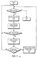
- FIG. 7 a flow chart is shown which outlines the method steps for storing IC design analysis results in the results register 28 of FIG. 6(a).
- CPU 15 starts the analysis of the IC layout with respect to a specific design rule.
- Reference graph register 24 entries (these are equivalently the individual group types 33 of results register 28) are sequentially selected in step 41 and conventionally analyzed with respect to a specific design rule in step 43.
- In-group results created 44 from this analysis are stored in in-group results register 35.
- the computer software program Dracula® from Cadence Design Systems, San Jose, California, is an example of programmed instruction steps which are stored in program memory 17 and executed by CPU 15 for analyzing design rules.
- CPU 15 determines in step 45 whether a rain relationship exists between the current reference graph register 24 entry and any of its lower level cell references. If no such relationship exists, that is, if the individual shape in the current reference graph 25 entry does not have the potential to generate override results 37, then no action is taken and CPU 15 returns to step 41 to evaluate the next reference graph 25 entry.
- the shapes from the current reference graph 25 entry do interact with lower-level shapes in such a manner as to impact the results of the analysis of those lower-level shapes, then the previous lower-level results are overridden in step 49.
- a reference to the override result is stored as an override result 37, and the result shape itself is placed in the shape model register 27 if it does not yet exist. Since this override entry replaces a specific shape or shapes from a cell reference lower in the design hierarchy than the current reference graph register 24 entry, the override result list must also include reference to the specific shapes replaced. Each such reference is defined by a shape model identifier, a stamping point and a rotation.
- step 51 a determination is made as to whether the new override shape has been previously stored in shape model register 27 as a library shape. If the shape has been previously added, the existing model is referenced, and this reference is added as an override result 37 entry associated with the group type 33 being evaluated. The CPU 15 then begins processing the next reference graph 25 entry again in step 41.
- step 51 If it is determined in step 51 that the resulting shape has not been previously stored in shape model register 27, the new shape is then stored 52 into the shape register.
- the new shape type 34 is used to represent the shape as an override result 37, of which it is a component.
- the CPU 15 then begins processing the next reference graph entry again in step 41.
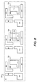
- shapes typical of an integrated circuit layout are arranged to form electrical circuit elements 61, 63, 65, 67, 69, and 71.
- the first four shapes (61-67) are each placed three times in the cell marked "A", whose bounding box 73 is depicted as a dashed rectangle surrounding the shapes.
- Shape 69 is placed once in A.
- Group A also references three instances of group B (B1, B2, and B3).
- the bounding box 75 for B is depicted by the dashed line surrounding shape 71.
- Shape 71 is the sole shape contained by group B.
- the reference graph for the circuit layout of FIG. 8 is pictorially shown in FIG. 9.
- the reference graph contains all groups in the design, namely groups A and B, with group B shown referenced three times by group A.
- a rain relationship exists between shape 69 of group A and group B2, because shape 69 covers some portion of the area within group B's bounding box 75.
- FIG. 10 a partial layout diagram of FIG. 8 is shown, illustrating an example design rule analysis in which an exclusive-OR (XOR) of the shapes of FIG. 8 is calculated.
- the exclusive-OR is defined as a logical binary operation in which two or more logical operands are compared, producing a logical "1" if any but not all of the operands are in a "1" state, and producing a logical "0" otherwise.
- the shaded areas represent an area which is circumscribed by the area of one shape (69) or the other (71), but not both. (Note that the center 77 is unshaded, since this center area is circumscribed by both shapes 69 and 71.)
- the in-group data for shapes 61, 63, 65 and 67 are first processed with respect to the XOR operation.
- the results created from this operation are the shapes 61, 63, 65 and 67.
- the resulting shapes are entered as in-group results 35.
- a rain-relationship is noted (as in step 45 of FIG. 7) between shape 69 in group A and shape 71 in lower-level group B.
- the XOR operation will modify shape 71 by virtue of its interaction with shape 69 in the higher level above it in the hierarchy.
Landscapes
- Engineering & Computer Science (AREA)
- Computer Hardware Design (AREA)
- Physics & Mathematics (AREA)
- Theoretical Computer Science (AREA)
- Evolutionary Computation (AREA)
- Geometry (AREA)
- General Engineering & Computer Science (AREA)
- General Physics & Mathematics (AREA)
- Design And Manufacture Of Integrated Circuits (AREA)
Applications Claiming Priority (3)
| Application Number | Priority Date | Filing Date | Title |
|---|---|---|---|
| US08/124,330 US5440720A (en) | 1993-09-20 | 1993-09-20 | Architecture and method for data reduction in a system for analyzing geometric databases |
| US124330 | 1993-09-20 | ||
| PCT/US1994/010626 WO1995008811A1 (en) | 1993-09-20 | 1994-09-20 | Data reduction in a system for analyzing geometric databases |
Publications (3)
| Publication Number | Publication Date |
|---|---|
| EP0721624A1 EP0721624A1 (en) | 1996-07-17 |
| EP0721624A4 EP0721624A4 (Direct) | 1996-08-07 |
| EP0721624B1 true EP0721624B1 (en) | 2000-06-14 |
Family
ID=22414239
Family Applications (1)
| Application Number | Title | Priority Date | Filing Date |
|---|---|---|---|
| EP94929263A Expired - Lifetime EP0721624B1 (en) | 1993-09-20 | 1994-09-20 | Data reduction in a system for analyzing geometric databases |
Country Status (4)
| Country | Link |
|---|---|
| US (1) | US5440720A (Direct) |
| EP (1) | EP0721624B1 (Direct) |
| DE (1) | DE69424944T2 (Direct) |
| WO (1) | WO1995008811A1 (Direct) |
Families Citing this family (50)
| Publication number | Priority date | Publication date | Assignee | Title |
|---|---|---|---|---|
| JPH07334372A (ja) * | 1993-12-24 | 1995-12-22 | Seiko Epson Corp | エミュレートシステム及びエミュレート方法 |
| US5559718A (en) * | 1994-04-28 | 1996-09-24 | Cadence Design Systems, Inc. | System and method for model-based verification of local design rules |
| US5903469A (en) * | 1994-11-08 | 1999-05-11 | Synopsys, Inc. | Method of extracting layout parasitics for nets of an integrated circuit using a connectivity-based approach |
| US5828580A (en) * | 1994-11-08 | 1998-10-27 | Epic Design Technology, Inc. | Connectivity-based approach for extracting parasitic layout in an integrated circuit |
| US5625564A (en) * | 1995-01-13 | 1997-04-29 | Cadence Design Systems, Inc. | System and method for hierarchical device extraction |
| US5629861A (en) * | 1995-05-19 | 1997-05-13 | International Business Machines Corporation | Nested maximum space computation and efficient generation of nested shape complementation |
| US7715642B1 (en) * | 1995-06-06 | 2010-05-11 | Hewlett-Packard Development Company, L.P. | Bitmap image compressing |
| US5740071A (en) * | 1995-06-07 | 1998-04-14 | International Business Machines Corporation | Method and apparatus for selective shape adjustment of hierarchical designs |
| US5726903A (en) * | 1996-02-07 | 1998-03-10 | Unisys Corporation | Method and apparatus for resolving conflicts between cell substitution recommendations provided by a drive strength adjust tool |
| US5812415A (en) * | 1996-04-05 | 1998-09-22 | Cadence Design Systems, Inc. | Method and apparatus for enhancing performance of design verification systems |
| US5887155A (en) * | 1996-07-25 | 1999-03-23 | Microunity Systems Engineering, Inc. | Vertex based geometry engine system for use in integrated circuit design |
| US5914889A (en) * | 1996-09-13 | 1999-06-22 | Lucent Technologies Inc. | Method and system for generating a mask layout of an optical integrated circuit |
| US6026220A (en) * | 1996-11-19 | 2000-02-15 | Unisys Corporation | Method and apparatus for incremntally optimizing a circuit design |
| US5980092A (en) * | 1996-11-19 | 1999-11-09 | Unisys Corporation | Method and apparatus for optimizing a gated clock structure using a standard optimization tool |
| US5956256A (en) * | 1996-11-19 | 1999-09-21 | Unisys Corporation | Method and apparatus for optimizing a circuit design having multi-paths therein |
| US5864487A (en) * | 1996-11-19 | 1999-01-26 | Unisys Corporation | Method and apparatus for identifying gated clocks within a circuit design using a standard optimization tool |
| US5960184A (en) * | 1996-11-19 | 1999-09-28 | Unisys Corporation | Method and apparatus for providing optimization parameters to a logic optimizer tool |
| US5802075A (en) * | 1997-01-16 | 1998-09-01 | Unisys Corporation | Distributed test pattern generation |
| US5912820A (en) * | 1997-01-22 | 1999-06-15 | Unisys Corporation | Method and apparatus for distributing a clock tree within a hierarchical circuit design |
| US6516456B1 (en) | 1997-01-27 | 2003-02-04 | Unisys Corporation | Method and apparatus for selectively viewing nets within a database editor tool |
| US6718520B1 (en) | 1997-01-27 | 2004-04-06 | Unisys Corporation | Method and apparatus for selectively providing hierarchy to a circuit design |
| US7076410B1 (en) | 1997-01-27 | 2006-07-11 | Unisys Corporation | Method and apparatus for efficiently viewing a number of selected components using a database editor tool |
| US6684376B1 (en) | 1997-01-27 | 2004-01-27 | Unisys Corporation | Method and apparatus for selecting components within a circuit design database |
| US6708144B1 (en) | 1997-01-27 | 2004-03-16 | Unisys Corporation | Spreadsheet driven I/O buffer synthesis process |
| US6910200B1 (en) | 1997-01-27 | 2005-06-21 | Unisys Corporation | Method and apparatus for associating selected circuit instances and for performing a group operation thereon |
| US6754879B1 (en) | 1997-01-27 | 2004-06-22 | Unisys Corporation | Method and apparatus for providing modularity to a behavioral description of a circuit design |
| US6701289B1 (en) | 1997-01-27 | 2004-03-02 | Unisys Corporation | Method and apparatus for using a placement tool to manipulate cell substitution lists |
| US6009250A (en) * | 1997-09-30 | 1999-12-28 | Synopsys, Inc. | Selective flattening in layout areas in computer implemented integrated circuit design |
| JPH11233581A (ja) * | 1998-02-13 | 1999-08-27 | Mitsubishi Electric Corp | ウェーハテスト方法 |
| US7340698B1 (en) | 1998-07-22 | 2008-03-04 | Magma Design Automation, Inc. | Method of estimating performance of integrated circuit designs by finding scalars for strongly coupled components |
| US6499129B1 (en) * | 1998-07-22 | 2002-12-24 | Circuit Semantics, Inc. | Method of estimating performance of integrated circuit designs |
| US6470477B1 (en) | 1999-12-23 | 2002-10-22 | Koninklijke Philips Electronics N.V. | Methods for converting features to a uniform micron technology in an integrated circuit design and apparatus for doing the same |
| US6539519B1 (en) * | 2000-05-31 | 2003-03-25 | Mark D. Meeker | Spatial characteristic and logical hierarchy based manner for compactly storing IC design data and related operations |
| US6889370B1 (en) | 2000-06-20 | 2005-05-03 | Unisys Corporation | Method and apparatus for selecting and aligning cells using a placement tool |
| US6546532B1 (en) | 2000-06-20 | 2003-04-08 | Unisys Corporation | Method and apparatus for traversing and placing cells using a placement tool |
| DE10149021B4 (de) * | 2001-09-28 | 2006-04-27 | Infineon Technologies Ag | Datenverarbeitungssystem zum Entwurf eines Layouts einer integrierten elektronischen Schaltung aus einer Vielzahl von elektronischen Bauelementen |
| US20030217026A1 (en) * | 2002-01-31 | 2003-11-20 | Steven Teig | Structure for storing a plurality os sub-networks |
| US6954910B2 (en) * | 2002-01-31 | 2005-10-11 | Cadence Design Systems, Inc. | Method and apparatus for producing a circuit description of a design |
| DE10206658B4 (de) * | 2002-02-15 | 2011-11-17 | Qimonda Ag | Verfahren zum Überprüfen einer integrierten elektrischen Schaltung |
| DE10245037B4 (de) * | 2002-09-26 | 2007-08-23 | Infineon Technologies Ag | Verfahren zum Entwurf von DRAM-Halbleiter-Speicherbauelementen |
| US6941527B2 (en) * | 2003-04-28 | 2005-09-06 | International Business Machines Corporation | Method, system and program product for reducing a size of a configuration database utilized to configure a hardware digital system |
| US7069534B2 (en) | 2003-12-17 | 2006-06-27 | Sahouria Emile Y | Mask creation with hierarchy management using cover cells |
| US7913206B1 (en) | 2004-09-16 | 2011-03-22 | Cadence Design Systems, Inc. | Method and mechanism for performing partitioning of DRC operations |
| US7904852B1 (en) | 2005-09-12 | 2011-03-08 | Cadence Design Systems, Inc. | Method and system for implementing parallel processing of electronic design automation tools |
| US8448096B1 (en) | 2006-06-30 | 2013-05-21 | Cadence Design Systems, Inc. | Method and system for parallel processing of IC design layouts |
| US8214775B2 (en) * | 2007-09-14 | 2012-07-03 | Luminescent Technologies, Inc. | System for determining repetitive work units |
| JP2009176049A (ja) * | 2008-01-24 | 2009-08-06 | Fujitsu Ltd | 解析支援装置、解析支援方法および解析支援プログラム |
| US20140177940A1 (en) * | 2011-08-03 | 2014-06-26 | Hitachi High-Technologies Corporation | Recipe generation apparatus, inspection support apparatus, inspection system, and recording media |
| US20190258396A1 (en) * | 2018-02-20 | 2019-08-22 | Adobe Inc. | Layout design with adaptive areas |
| JP7278795B2 (ja) * | 2019-02-21 | 2023-05-22 | キヤノン株式会社 | 画像処理装置、画像処理方法及びプログラム |
Family Cites Families (15)
| Publication number | Priority date | Publication date | Assignee | Title |
|---|---|---|---|---|
| US5050091A (en) * | 1985-02-28 | 1991-09-17 | Electric Editor, Inc. | Integrated electric design system with automatic constraint satisfaction |
| US4831543A (en) * | 1986-02-21 | 1989-05-16 | Harris Semiconductor (Patents) Inc. | Hierarchical net list derivation system |
| US5212650A (en) * | 1986-09-12 | 1993-05-18 | Digital Equipment Corporation | Procedure and data structure for synthesis and transformation of logic circuit designs |
| US5150308A (en) * | 1986-09-12 | 1992-09-22 | Digital Equipment Corporation | Parameter and rule creation and modification mechanism for use by a procedure for synthesis of logic circuit designs |
| US4924385A (en) * | 1987-10-26 | 1990-05-08 | Casio Computer Co., Ltd. | Method of detecting types of parts constituting a larger group of parts |
| US5301318A (en) * | 1988-05-13 | 1994-04-05 | Silicon Systems, Inc. | Hierarchical netlist extraction tool |
| KR930007749B1 (ko) * | 1988-05-25 | 1993-08-18 | 마쯔시다덴기산교 가부시기가이샤 | 제품생산 계획형 추론장치 |
| US4967367A (en) * | 1988-11-21 | 1990-10-30 | Vlsi Technology, Inc. | Synthetic netlist system and method |
| US5202841A (en) * | 1989-07-14 | 1993-04-13 | Mitsubishi Denki Kabushiki Kaisha | Layout pattern verification system |
| US5231590A (en) * | 1989-10-13 | 1993-07-27 | Zilog, Inc. | Technique for modifying an integrated circuit layout |
| US5249265A (en) * | 1989-10-24 | 1993-09-28 | International Business Machines Corporation | Structure storage management in a graphics display device |
| US5210699A (en) * | 1989-12-18 | 1993-05-11 | Siemens Components, Inc. | Process for extracting logic from transistor and resistor data representations of circuits |
| US5278769A (en) * | 1991-04-12 | 1994-01-11 | Lsi Logic Corporation | Automatic logic model generation from schematic data base |
| US5303161A (en) * | 1990-12-10 | 1994-04-12 | Hughes Aircraft Company | Technology independent integrated circuit mask artwork generator |
| US5349659A (en) * | 1992-01-23 | 1994-09-20 | Cadence Design Systems, Inc. | Hierarchical ordering of logical elements in the canonical mapping of net lists |
-
1993
- 1993-09-20 US US08/124,330 patent/US5440720A/en not_active Expired - Lifetime
-
1994
- 1994-09-20 WO PCT/US1994/010626 patent/WO1995008811A1/en not_active Ceased
- 1994-09-20 EP EP94929263A patent/EP0721624B1/en not_active Expired - Lifetime
- 1994-09-20 DE DE69424944T patent/DE69424944T2/de not_active Expired - Lifetime
Also Published As
| Publication number | Publication date |
|---|---|
| DE69424944T2 (de) | 2000-10-19 |
| EP0721624A4 (Direct) | 1996-08-07 |
| EP0721624A1 (en) | 1996-07-17 |
| DE69424944D1 (de) | 2000-07-20 |
| WO1995008811A1 (en) | 1995-03-30 |
| US5440720A (en) | 1995-08-08 |
Similar Documents
| Publication | Publication Date | Title |
|---|---|---|
| EP0721624B1 (en) | Data reduction in a system for analyzing geometric databases | |
| US5818729A (en) | Method and system for placing cells using quadratic placement and a spanning tree model | |
| US5696693A (en) | Method for placing logic functions and cells in a logic design using floor planning by analogy | |
| US6189130B1 (en) | System and method for determining density maps in hierarchical designs | |
| EP0757819B1 (en) | System and method for model-based verification of local design rules | |
| US6009250A (en) | Selective flattening in layout areas in computer implemented integrated circuit design | |
| US6493658B1 (en) | Optimization processing for integrated circuit physical design automation system using optimally switched fitness improvement algorithms | |
| US6536023B1 (en) | Method and system for hierarchical metal-end, enclosure and exposure checking | |
| US5581474A (en) | Identifying overconstraints using port abstraction graphs | |
| US6598211B2 (en) | Scaleable approach to extracting bridges from a hierarchically described VLSI layout | |
| US20030088839A1 (en) | Method of designing integrated circuit and apparatus for designing integrated circuit | |
| JPH03156572A (ja) | 論理回路比較検証システムおよび方法 | |
| WO2000065492A1 (en) | Method for storing multiple levels of design data in a common database | |
| CN114861590B (zh) | 一种应用于大规模版图数据的索引方法 | |
| US6167555A (en) | System and method for converting polygon-based wires of an integrated circuit design to path-based wires | |
| US20070011637A1 (en) | Method and system for performing local geometrical operation on a hierarchical layout of a semiconductor device | |
| CN115293078B (zh) | 集成电路的节点改写方法、装置、电子设备及介质 | |
| Jiménez-González et al. | CC-Radix: a cache conscious sorting based on Radix sort | |
| Lin et al. | Module placement with boundary constraints using B*-trees | |
| JPH06124202A (ja) | プログラムを実行するためのデジタル信号処理装置 | |
| US12481816B2 (en) | Constraint file-based novel framework for net-based checking technique | |
| US12032894B2 (en) | System and method for synchronizing net text across hierarchical levels | |
| US6189129B1 (en) | Figure operation of layout for high speed processing | |
| US12361509B1 (en) | Semiconductor process simulation on graphics processing unit (GPU) with multi-level data structure | |
| Hedenstierna et al. | The use of inverse layout trees for hierarchical design rule checking |
Legal Events
| Date | Code | Title | Description |
|---|---|---|---|
| PUAI | Public reference made under article 153(3) epc to a published international application that has entered the european phase |
Free format text: ORIGINAL CODE: 0009012 |
|
| 17P | Request for examination filed |
Effective date: 19960403 |
|
| AK | Designated contracting states |
Kind code of ref document: A1 Designated state(s): DE ES FR GB IT |
|
| A4 | Supplementary search report drawn up and despatched |
Effective date: 19960620 |
|
| AK | Designated contracting states |
Kind code of ref document: A4 Designated state(s): DE ES FR GB IT |
|
| GRAG | Despatch of communication of intention to grant |
Free format text: ORIGINAL CODE: EPIDOS AGRA |
|
| 17Q | First examination report despatched |
Effective date: 19990802 |
|
| GRAG | Despatch of communication of intention to grant |
Free format text: ORIGINAL CODE: EPIDOS AGRA |
|
| GRAH | Despatch of communication of intention to grant a patent |
Free format text: ORIGINAL CODE: EPIDOS IGRA |
|
| GRAH | Despatch of communication of intention to grant a patent |
Free format text: ORIGINAL CODE: EPIDOS IGRA |
|
| GRAA | (expected) grant |
Free format text: ORIGINAL CODE: 0009210 |
|
| AK | Designated contracting states |
Kind code of ref document: B1 Designated state(s): DE ES FR GB IT |
|
| PG25 | Lapsed in a contracting state [announced via postgrant information from national office to epo] |
Ref country code: IT Free format text: LAPSE BECAUSE OF FAILURE TO SUBMIT A TRANSLATION OF THE DESCRIPTION OR TO PAY THE FEE WITHIN THE PRESCRIBED TIME-LIMIT;WARNING: LAPSES OF ITALIAN PATENTS WITH EFFECTIVE DATE BEFORE 2007 MAY HAVE OCCURRED AT ANY TIME BEFORE 2007. THE CORRECT EFFECTIVE DATE MAY BE DIFFERENT FROM THE ONE RECORDED. Effective date: 20000614 Ref country code: ES Free format text: THE PATENT HAS BEEN ANNULLED BY A DECISION OF A NATIONAL AUTHORITY Effective date: 20000614 |
|
| REF | Corresponds to: |
Ref document number: 69424944 Country of ref document: DE Date of ref document: 20000720 |
|
| ET | Fr: translation filed | ||
| PLBE | No opposition filed within time limit |
Free format text: ORIGINAL CODE: 0009261 |
|
| STAA | Information on the status of an ep patent application or granted ep patent |
Free format text: STATUS: NO OPPOSITION FILED WITHIN TIME LIMIT |
|
| 26N | No opposition filed | ||
| REG | Reference to a national code |
Ref country code: GB Ref legal event code: IF02 |
|
| PGFP | Annual fee paid to national office [announced via postgrant information from national office to epo] |
Ref country code: GB Payment date: 20120925 Year of fee payment: 19 |
|
| PGFP | Annual fee paid to national office [announced via postgrant information from national office to epo] |
Ref country code: FR Payment date: 20121001 Year of fee payment: 19 |
|
| PGFP | Annual fee paid to national office [announced via postgrant information from national office to epo] |
Ref country code: DE Payment date: 20120927 Year of fee payment: 19 |
|
| GBPC | Gb: european patent ceased through non-payment of renewal fee |
Effective date: 20130920 |
|
| REG | Reference to a national code |
Ref country code: DE Ref legal event code: R119 Ref document number: 69424944 Country of ref document: DE Effective date: 20140401 |
|
| REG | Reference to a national code |
Ref country code: FR Ref legal event code: ST Effective date: 20140530 |
|
| PG25 | Lapsed in a contracting state [announced via postgrant information from national office to epo] |
Ref country code: GB Free format text: LAPSE BECAUSE OF NON-PAYMENT OF DUE FEES Effective date: 20130920 |
|
| PG25 | Lapsed in a contracting state [announced via postgrant information from national office to epo] |
Ref country code: DE Free format text: LAPSE BECAUSE OF NON-PAYMENT OF DUE FEES Effective date: 20140401 Ref country code: FR Free format text: LAPSE BECAUSE OF NON-PAYMENT OF DUE FEES Effective date: 20130930 |