EP0721624B1 - Data reduction in a system for analyzing geometric databases - Google Patents
Data reduction in a system for analyzing geometric databases Download PDFInfo
- Publication number
- EP0721624B1 EP0721624B1 EP94929263A EP94929263A EP0721624B1 EP 0721624 B1 EP0721624 B1 EP 0721624B1 EP 94929263 A EP94929263 A EP 94929263A EP 94929263 A EP94929263 A EP 94929263A EP 0721624 B1 EP0721624 B1 EP 0721624B1
- Authority
- EP
- European Patent Office
- Prior art keywords
- group
- shape
- model
- models
- result
- Prior art date
- Legal status (The legal status is an assumption and is not a legal conclusion. Google has not performed a legal analysis and makes no representation as to the accuracy of the status listed.)
- Expired - Lifetime
Links
Images


Classifications
-
- G—PHYSICS
- G06—COMPUTING; CALCULATING OR COUNTING
- G06F—ELECTRIC DIGITAL DATA PROCESSING
- G06F30/00—Computer-aided design [CAD]
- G06F30/30—Circuit design
- G06F30/39—Circuit design at the physical level
- G06F30/398—Design verification or optimisation, e.g. using design rule check [DRC], layout versus schematics [LVS] or finite element methods [FEM]
Description
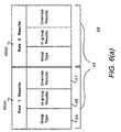
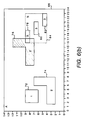
- Shape 1: (0,0), (0,2), (2,2), (2,0)
- Shape 2: (0,0), (0,1), (4,1), (1,5), (5,5), (5,0)
- Shape 3: (0,0), (0,1), (3,1), (3,0)
Claims (8)
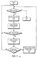
- A method for data storage requirement reduction in a system for analyzing a geometric database, wherein the method comprises the steps of:(a) reading a listing of group models comprising the geometric database include said group models referencing shape models and/or group models, whereby shape models represent the lowest level components, to be found after claim 8;(b) performing a design rule verification upon a set of shape models referenced by a first group model within the listing with respect to a specific design rule, thereby generating an in-group result, where the in-group result is derived from the set of shape models found within the first group model; said method characterised by the following steps:(c) determining whether a rain relationship exists, the rain relationship existing when a spatial relationship between a shape model within the first group model invalidates a lower-level verification result; and(d) creating an override result if a rain relationship exists, wherein the override result references a shape model created during a design rule verification performed upon those shape models causing the rain relationship,
wherein a design rule verification result is not duplicated in said geometric database. - The method for data storage requirement reduction according to Claim 1, wherein the design rule analysis of step (b) is performed according a conventional software program.
- The method for data storage requirement reduction according to Claim 1, wherein if it is determined in step (c) that no rain relationship exists, a next group model is analyzed in step (b).
- The method for data storage requirement reduction according to Claim 1, wherein the step of analyzing the first group model with respect to a specific design rule further comprises the step of creating and storing in-group results.
- The method for data storage requirement reduction of claim 1, further comprising the step of:(e) storing a newly-created shape model corresponding to an override shape in a shape model register.
- The method for data storage requirement reduction of claim 1, further comprising the step of:(e) repeating steps (b) through (d) for a next group model in the geometric database.
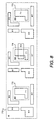
- An apparatus for data storage requirement reduction in a system for analyzing a geometric database include said group models referencing shape models and/or group models, whereby shape models represent the lowest level components, to be found after claim 8, wherein the means for data storage requirement reduction comprises:means for reading a listing of group models comprising the geometric database;means for performing a design rule verification upon a set of shape models referenced by a first group model within the listing with respect to a specific design rule, thereby generating an in-group result, where the in-group result is derived from the set of shape models found within the first group model;said apparatus characterised bymeans for determining whether a rain relationship exists, the rain relationship existing when a spatial relationship between a shape model within the first group model invalidates a lower-level verification result; andmeans for creating an override result if a rain relationship exists, wherein the override result references a shape model created during a design rule verification performed upon those shape models causing the rain relationship,
wherein a design rule verification result is not duplicated in said geometric database. - The apparatus for data storage requirement reduction of claim 7, further comprising a means for storing a newly-created shape model corresponding to an override shape in a shape model register.
Applications Claiming Priority (3)
| Application Number | Priority Date | Filing Date | Title |
|---|---|---|---|
| US08/124,330 US5440720A (en) | 1993-09-20 | 1993-09-20 | Architecture and method for data reduction in a system for analyzing geometric databases |
| PCT/US1994/010626 WO1995008811A1 (en) | 1993-09-20 | 1994-09-20 | Data reduction in a system for analyzing geometric databases |
| US124330 | 1998-07-29 |
Publications (3)
| Publication Number | Publication Date |
|---|---|
| EP0721624A1 EP0721624A1 (en) | 1996-07-17 |
| EP0721624A4 EP0721624A4 (en) | 1996-08-07 |
| EP0721624B1 true EP0721624B1 (en) | 2000-06-14 |
Family
ID=22414239
Family Applications (1)
| Application Number | Title | Priority Date | Filing Date |
|---|---|---|---|
| EP94929263A Expired - Lifetime EP0721624B1 (en) | 1993-09-20 | 1994-09-20 | Data reduction in a system for analyzing geometric databases |
Country Status (4)
| Country | Link |
|---|---|
| US (1) | US5440720A (en) |
| EP (1) | EP0721624B1 (en) |
| DE (1) | DE69424944T2 (en) |
| WO (1) | WO1995008811A1 (en) |
Families Citing this family (50)
| Publication number | Priority date | Publication date | Assignee | Title |
|---|---|---|---|---|
| JPH07334372A (en) * | 1993-12-24 | 1995-12-22 | Seiko Epson Corp | System and method for emulation |
| US5559718A (en) * | 1994-04-28 | 1996-09-24 | Cadence Design Systems, Inc. | System and method for model-based verification of local design rules |
| US5903469A (en) | 1994-11-08 | 1999-05-11 | Synopsys, Inc. | Method of extracting layout parasitics for nets of an integrated circuit using a connectivity-based approach |
| US5828580A (en) * | 1994-11-08 | 1998-10-27 | Epic Design Technology, Inc. | Connectivity-based approach for extracting parasitic layout in an integrated circuit |
| US5625564A (en) * | 1995-01-13 | 1997-04-29 | Cadence Design Systems, Inc. | System and method for hierarchical device extraction |
| US5629861A (en) * | 1995-05-19 | 1997-05-13 | International Business Machines Corporation | Nested maximum space computation and efficient generation of nested shape complementation |
| US7715642B1 (en) * | 1995-06-06 | 2010-05-11 | Hewlett-Packard Development Company, L.P. | Bitmap image compressing |
| US5740071A (en) * | 1995-06-07 | 1998-04-14 | International Business Machines Corporation | Method and apparatus for selective shape adjustment of hierarchical designs |
| US5726903A (en) * | 1996-02-07 | 1998-03-10 | Unisys Corporation | Method and apparatus for resolving conflicts between cell substitution recommendations provided by a drive strength adjust tool |
| US5812415A (en) * | 1996-04-05 | 1998-09-22 | Cadence Design Systems, Inc. | Method and apparatus for enhancing performance of design verification systems |
| US5887155A (en) * | 1996-07-25 | 1999-03-23 | Microunity Systems Engineering, Inc. | Vertex based geometry engine system for use in integrated circuit design |
| US5914889A (en) * | 1996-09-13 | 1999-06-22 | Lucent Technologies Inc. | Method and system for generating a mask layout of an optical integrated circuit |
| US5980092A (en) * | 1996-11-19 | 1999-11-09 | Unisys Corporation | Method and apparatus for optimizing a gated clock structure using a standard optimization tool |
| US5864487A (en) * | 1996-11-19 | 1999-01-26 | Unisys Corporation | Method and apparatus for identifying gated clocks within a circuit design using a standard optimization tool |
| US6026220A (en) * | 1996-11-19 | 2000-02-15 | Unisys Corporation | Method and apparatus for incremntally optimizing a circuit design |
| US5956256A (en) * | 1996-11-19 | 1999-09-21 | Unisys Corporation | Method and apparatus for optimizing a circuit design having multi-paths therein |
| US5960184A (en) * | 1996-11-19 | 1999-09-28 | Unisys Corporation | Method and apparatus for providing optimization parameters to a logic optimizer tool |
| US5802075A (en) * | 1997-01-16 | 1998-09-01 | Unisys Corporation | Distributed test pattern generation |
| US5912820A (en) * | 1997-01-22 | 1999-06-15 | Unisys Corporation | Method and apparatus for distributing a clock tree within a hierarchical circuit design |
| US7076410B1 (en) | 1997-01-27 | 2006-07-11 | Unisys Corporation | Method and apparatus for efficiently viewing a number of selected components using a database editor tool |
| US6754879B1 (en) | 1997-01-27 | 2004-06-22 | Unisys Corporation | Method and apparatus for providing modularity to a behavioral description of a circuit design |
| US6910200B1 (en) | 1997-01-27 | 2005-06-21 | Unisys Corporation | Method and apparatus for associating selected circuit instances and for performing a group operation thereon |
| US6708144B1 (en) | 1997-01-27 | 2004-03-16 | Unisys Corporation | Spreadsheet driven I/O buffer synthesis process |
| US6701289B1 (en) | 1997-01-27 | 2004-03-02 | Unisys Corporation | Method and apparatus for using a placement tool to manipulate cell substitution lists |
| US6684376B1 (en) | 1997-01-27 | 2004-01-27 | Unisys Corporation | Method and apparatus for selecting components within a circuit design database |
| US6718520B1 (en) | 1997-01-27 | 2004-04-06 | Unisys Corporation | Method and apparatus for selectively providing hierarchy to a circuit design |
| US6516456B1 (en) | 1997-01-27 | 2003-02-04 | Unisys Corporation | Method and apparatus for selectively viewing nets within a database editor tool |
| US6009250A (en) * | 1997-09-30 | 1999-12-28 | Synopsys, Inc. | Selective flattening in layout areas in computer implemented integrated circuit design |
| JPH11233581A (en) * | 1998-02-13 | 1999-08-27 | Mitsubishi Electric Corp | Wafer testing method |
| US6499129B1 (en) * | 1998-07-22 | 2002-12-24 | Circuit Semantics, Inc. | Method of estimating performance of integrated circuit designs |
| US7117461B1 (en) | 1998-07-22 | 2006-10-03 | Magma Design Automation, Inc. | Method of estimating performance of integrated circuit designs using state point identification |
| US6470477B1 (en) | 1999-12-23 | 2002-10-22 | Koninklijke Philips Electronics N.V. | Methods for converting features to a uniform micron technology in an integrated circuit design and apparatus for doing the same |
| US6539519B1 (en) * | 2000-05-31 | 2003-03-25 | Mark D. Meeker | Spatial characteristic and logical hierarchy based manner for compactly storing IC design data and related operations |
| US6546532B1 (en) | 2000-06-20 | 2003-04-08 | Unisys Corporation | Method and apparatus for traversing and placing cells using a placement tool |
| US6889370B1 (en) * | 2000-06-20 | 2005-05-03 | Unisys Corporation | Method and apparatus for selecting and aligning cells using a placement tool |
| DE10149021B4 (en) * | 2001-09-28 | 2006-04-27 | Infineon Technologies Ag | Data processing system for designing a layout of an integrated electronic circuit of a plurality of electronic components |
| US7100143B2 (en) * | 2002-01-31 | 2006-08-29 | Cadence Design Systems, Inc. | Method and apparatus for pre-tabulating sub-networks |
| US20030217026A1 (en) * | 2002-01-31 | 2003-11-20 | Steven Teig | Structure for storing a plurality os sub-networks |
| DE10206658B4 (en) * | 2002-02-15 | 2011-11-17 | Qimonda Ag | Method for checking an integrated electrical circuit |
| DE10245037B4 (en) * | 2002-09-26 | 2007-08-23 | Infineon Technologies Ag | Method of designing DRAM semiconductor memory devices |
| US6941527B2 (en) * | 2003-04-28 | 2005-09-06 | International Business Machines Corporation | Method, system and program product for reducing a size of a configuration database utilized to configure a hardware digital system |
| US7069534B2 (en) * | 2003-12-17 | 2006-06-27 | Sahouria Emile Y | Mask creation with hierarchy management using cover cells |
| US7913206B1 (en) | 2004-09-16 | 2011-03-22 | Cadence Design Systems, Inc. | Method and mechanism for performing partitioning of DRC operations |
| US7904852B1 (en) | 2005-09-12 | 2011-03-08 | Cadence Design Systems, Inc. | Method and system for implementing parallel processing of electronic design automation tools |
| US8448096B1 (en) | 2006-06-30 | 2013-05-21 | Cadence Design Systems, Inc. | Method and system for parallel processing of IC design layouts |
| US8214775B2 (en) * | 2007-09-14 | 2012-07-03 | Luminescent Technologies, Inc. | System for determining repetitive work units |
| JP2009176049A (en) * | 2008-01-24 | 2009-08-06 | Fujitsu Ltd | Analysis support device, analysis support method, and analysis support program |
| US20140177940A1 (en) * | 2011-08-03 | 2014-06-26 | Hitachi High-Technologies Corporation | Recipe generation apparatus, inspection support apparatus, inspection system, and recording media |
| US20190258396A1 (en) * | 2018-02-20 | 2019-08-22 | Adobe Inc. | Layout design with adaptive areas |
| JP7278795B2 (en) * | 2019-02-21 | 2023-05-22 | キヤノン株式会社 | Image processing device, image processing method and program |
Family Cites Families (15)
| Publication number | Priority date | Publication date | Assignee | Title |
|---|---|---|---|---|
| US5050091A (en) * | 1985-02-28 | 1991-09-17 | Electric Editor, Inc. | Integrated electric design system with automatic constraint satisfaction |
| US4831543A (en) * | 1986-02-21 | 1989-05-16 | Harris Semiconductor (Patents) Inc. | Hierarchical net list derivation system |
| US5150308A (en) * | 1986-09-12 | 1992-09-22 | Digital Equipment Corporation | Parameter and rule creation and modification mechanism for use by a procedure for synthesis of logic circuit designs |
| US5212650A (en) * | 1986-09-12 | 1993-05-18 | Digital Equipment Corporation | Procedure and data structure for synthesis and transformation of logic circuit designs |
| US4924385A (en) * | 1987-10-26 | 1990-05-08 | Casio Computer Co., Ltd. | Method of detecting types of parts constituting a larger group of parts |
| US5301318A (en) * | 1988-05-13 | 1994-04-05 | Silicon Systems, Inc. | Hierarchical netlist extraction tool |
| KR930007749B1 (en) * | 1988-05-25 | 1993-08-18 | 마쯔시다덴기산교 가부시기가이샤 | Apparatus for inferring planning types of manufacturing |
| US4967367A (en) * | 1988-11-21 | 1990-10-30 | Vlsi Technology, Inc. | Synthetic netlist system and method |
| US5202841A (en) * | 1989-07-14 | 1993-04-13 | Mitsubishi Denki Kabushiki Kaisha | Layout pattern verification system |
| US5231590A (en) * | 1989-10-13 | 1993-07-27 | Zilog, Inc. | Technique for modifying an integrated circuit layout |
| US5249265A (en) * | 1989-10-24 | 1993-09-28 | International Business Machines Corporation | Structure storage management in a graphics display device |
| US5210699A (en) * | 1989-12-18 | 1993-05-11 | Siemens Components, Inc. | Process for extracting logic from transistor and resistor data representations of circuits |
| US5278769A (en) * | 1991-04-12 | 1994-01-11 | Lsi Logic Corporation | Automatic logic model generation from schematic data base |
| US5303161A (en) * | 1990-12-10 | 1994-04-12 | Hughes Aircraft Company | Technology independent integrated circuit mask artwork generator |
| US5349659A (en) * | 1992-01-23 | 1994-09-20 | Cadence Design Systems, Inc. | Hierarchical ordering of logical elements in the canonical mapping of net lists |
-
1993
- 1993-09-20 US US08/124,330 patent/US5440720A/en not_active Expired - Lifetime
-
1994
- 1994-09-20 DE DE69424944T patent/DE69424944T2/en not_active Expired - Lifetime
- 1994-09-20 EP EP94929263A patent/EP0721624B1/en not_active Expired - Lifetime
- 1994-09-20 WO PCT/US1994/010626 patent/WO1995008811A1/en active IP Right Grant
Also Published As
| Publication number | Publication date |
|---|---|
| WO1995008811A1 (en) | 1995-03-30 |
| US5440720A (en) | 1995-08-08 |
| EP0721624A4 (en) | 1996-08-07 |
| EP0721624A1 (en) | 1996-07-17 |
| DE69424944D1 (en) | 2000-07-20 |
| DE69424944T2 (en) | 2000-10-19 |
Similar Documents
| Publication | Publication Date | Title |
|---|---|---|
| EP0721624B1 (en) | Data reduction in a system for analyzing geometric databases | |
| US5818729A (en) | Method and system for placing cells using quadratic placement and a spanning tree model | |
| US5696693A (en) | Method for placing logic functions and cells in a logic design using floor planning by analogy | |
| US6189130B1 (en) | System and method for determining density maps in hierarchical designs | |
| US6011911A (en) | Layout overlap detection with selective flattening in computer implemented integrated circuit design | |
| EP0757819B1 (en) | System and method for model-based verification of local design rules | |
| US6009250A (en) | Selective flattening in layout areas in computer implemented integrated circuit design | |
| CA2308707C (en) | Polygon representation in an integrated circuit layout | |
| US6505328B1 (en) | Method for storing multiple levels of design data in a common database | |
| US20010052062A1 (en) | Parallel computer within dynamic random access memory | |
| US5581474A (en) | Identifying overconstraints using port abstraction graphs | |
| US20030088839A1 (en) | Method of designing integrated circuit and apparatus for designing integrated circuit | |
| US6598211B2 (en) | Scaleable approach to extracting bridges from a hierarchically described VLSI layout | |
| US20070011637A1 (en) | Method and system for performing local geometrical operation on a hierarchical layout of a semiconductor device | |
| JPH03156572A (en) | System and method for comparing and verifying logic circuit | |
| WO2002003261A1 (en) | Method and system for hierarchical metal-end, enclosure and exposure checking | |
| US6167555A (en) | System and method for converting polygon-based wires of an integrated circuit design to path-based wires | |
| US5319743A (en) | Intelligent and compact bucketing method for region queries in two-dimensional space | |
| JPH06124202A (en) | Digital signal processor for executing program | |
| Lin et al. | Module placement with boundary constraints using B*-trees | |
| US6189129B1 (en) | Figure operation of layout for high speed processing | |
| US6704915B1 (en) | Process for fast cell placement in integrated circuit design | |
| JPH07287051A (en) | Input data creation device for logic simulation | |
| Hedenstierna et al. | The use of inverse layout trees for hierarchical design rule checking | |
| US11630934B1 (en) | Integrated circuit analysis using a multi-level data hierarchy implemented on a distributed compute and data infrastructure |
Legal Events
| Date | Code | Title | Description |
|---|---|---|---|
| PUAI | Public reference made under article 153(3) epc to a published international application that has entered the european phase |
Free format text: ORIGINAL CODE: 0009012 |
|
| 17P | Request for examination filed |
Effective date: 19960403 |
|
| AK | Designated contracting states |
Kind code of ref document: A1 Designated state(s): DE ES FR GB IT |
|
| A4 | Supplementary search report drawn up and despatched |
Effective date: 19960620 |
|
| AK | Designated contracting states |
Kind code of ref document: A4 Designated state(s): DE ES FR GB IT |
|
| GRAG | Despatch of communication of intention to grant |
Free format text: ORIGINAL CODE: EPIDOS AGRA |
|
| 17Q | First examination report despatched |
Effective date: 19990802 |
|
| GRAG | Despatch of communication of intention to grant |
Free format text: ORIGINAL CODE: EPIDOS AGRA |
|
| GRAH | Despatch of communication of intention to grant a patent |
Free format text: ORIGINAL CODE: EPIDOS IGRA |
|
| GRAH | Despatch of communication of intention to grant a patent |
Free format text: ORIGINAL CODE: EPIDOS IGRA |
|
| GRAA | (expected) grant |
Free format text: ORIGINAL CODE: 0009210 |
|
| AK | Designated contracting states |
Kind code of ref document: B1 Designated state(s): DE ES FR GB IT |
|
| PG25 | Lapsed in a contracting state [announced via postgrant information from national office to epo] |
Ref country code: IT Free format text: LAPSE BECAUSE OF FAILURE TO SUBMIT A TRANSLATION OF THE DESCRIPTION OR TO PAY THE FEE WITHIN THE PRESCRIBED TIME-LIMIT;WARNING: LAPSES OF ITALIAN PATENTS WITH EFFECTIVE DATE BEFORE 2007 MAY HAVE OCCURRED AT ANY TIME BEFORE 2007. THE CORRECT EFFECTIVE DATE MAY BE DIFFERENT FROM THE ONE RECORDED. Effective date: 20000614 Ref country code: ES Free format text: THE PATENT HAS BEEN ANNULLED BY A DECISION OF A NATIONAL AUTHORITY Effective date: 20000614 |
|
| REF | Corresponds to: |
Ref document number: 69424944 Country of ref document: DE Date of ref document: 20000720 |
|
| ET | Fr: translation filed | ||
| PLBE | No opposition filed within time limit |
Free format text: ORIGINAL CODE: 0009261 |
|
| STAA | Information on the status of an ep patent application or granted ep patent |
Free format text: STATUS: NO OPPOSITION FILED WITHIN TIME LIMIT |
|
| 26N | No opposition filed | ||
| REG | Reference to a national code |
Ref country code: GB Ref legal event code: IF02 |
|
| PGFP | Annual fee paid to national office [announced via postgrant information from national office to epo] |
Ref country code: GB Payment date: 20120925 Year of fee payment: 19 |
|
| PGFP | Annual fee paid to national office [announced via postgrant information from national office to epo] |
Ref country code: FR Payment date: 20121001 Year of fee payment: 19 |
|
| PGFP | Annual fee paid to national office [announced via postgrant information from national office to epo] |
Ref country code: DE Payment date: 20120927 Year of fee payment: 19 |
|
| GBPC | Gb: european patent ceased through non-payment of renewal fee |
Effective date: 20130920 |
|
| REG | Reference to a national code |
Ref country code: DE Ref legal event code: R119 Ref document number: 69424944 Country of ref document: DE Effective date: 20140401 |
|
| REG | Reference to a national code |
Ref country code: FR Ref legal event code: ST Effective date: 20140530 |
|
| PG25 | Lapsed in a contracting state [announced via postgrant information from national office to epo] |
Ref country code: GB Free format text: LAPSE BECAUSE OF NON-PAYMENT OF DUE FEES Effective date: 20130920 |
|
| PG25 | Lapsed in a contracting state [announced via postgrant information from national office to epo] |
Ref country code: DE Free format text: LAPSE BECAUSE OF NON-PAYMENT OF DUE FEES Effective date: 20140401 Ref country code: FR Free format text: LAPSE BECAUSE OF NON-PAYMENT OF DUE FEES Effective date: 20130930 |