EP0721624B1 - Datenreduktion in einem system zur analysierung von geometrischen datenbanken - Google Patents
Datenreduktion in einem system zur analysierung von geometrischen datenbanken Download PDFInfo
- Publication number
- EP0721624B1 EP0721624B1 EP94929263A EP94929263A EP0721624B1 EP 0721624 B1 EP0721624 B1 EP 0721624B1 EP 94929263 A EP94929263 A EP 94929263A EP 94929263 A EP94929263 A EP 94929263A EP 0721624 B1 EP0721624 B1 EP 0721624B1
- Authority
- EP
- European Patent Office
- Prior art keywords
- group
- shape
- model
- models
- result
- Prior art date
- Legal status (The legal status is an assumption and is not a legal conclusion. Google has not performed a legal analysis and makes no representation as to the accuracy of the status listed.)
- Expired - Lifetime
Links
Images


Classifications
-
- G—PHYSICS
- G06—COMPUTING; CALCULATING OR COUNTING
- G06F—ELECTRIC DIGITAL DATA PROCESSING
- G06F30/00—Computer-aided design [CAD]
- G06F30/30—Circuit design
- G06F30/39—Circuit design at the physical level
- G06F30/398—Design verification or optimisation, e.g. using design rule check [DRC], layout versus schematics [LVS] or finite element methods [FEM]
Claims (8)
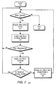
- Verfahren zur Reduktion der Datenspeicher-Erfordernisse in einem System zur Analysierung einer geometrischen Datenbank, wobei das Verfahren die folgenden Schritte umfaßt:(a) Auslesen einer Liste von Gruppenmodellen der geometrischen Datenbank, wobei die Gruppenmodelle sich auf Formmodelle und/oder Gruppenmodelle beziehen und die Formmodelle die Komponenten mit dem niedrigsten Niveau repräsentieren;(b) es wird eine Designregel-Verifikation auf einer Gruppe von Formmodellen durchgeführt, die auf ein erstes Gruppenmodell innerhalb der Liste unter Bezug auf eine spezielle Designregel bezogen sind, wodurch ein gruppeneigenes Ergebnis erzeugt wird, wobei das gruppeneigene Ergebnis von der Gruppe von Formmodellen abgeleitet wird, die sich innerhalb des ersten Gruppenmodells gefunden haben;
wobei das Verfahren durch die folgenden Schritte charakterisiert ist:(c) es wird bestimmt, ob eine Rain-Beziehung besteht, wobei die Rain-Beziehung existiert, wenn eine räumliche Beziehung zwischen einem Formmodell innerhalb des ersten Gruppenmodells ein Verifikationsergebnis mit niedrigerem Niveau ungültig macht; und(d) es wird ein Übersteuerungsergebnis erzeugt, wenn eine Rain-Beziehung vorhanden ist, wobei das Übersteuerungsergebnis sich auf ein Formmodell bezieht, das während einer Designregel-Verifikation erzeugt wurde, die auf jenen Formmodellen durchgeführt wurde, welche die Rain-Beziehung verursachten,
wobei ein Designregel-Verifikationsergebnis in der geometrischen Datenbank nicht dupliziert wird. - Verfahren zur Reduzierung der Datenspeicher-Erfordernisse nach Anspruch 1, bei welchem die Disignregelanalyse gemäß Schritt (b) gemäß einem herkömmlichen Software-Programm durchgeführt wird.
- Verfahren zur Reduzierung der Datenspeicher-Erfordernisse nach Anspruch 1, bei welchem dann, wenn im Schritt (c) bestimmt wird, daß keine Rain-Beziehung existiert, ein nächstes Gruppenmodell in Schritt (b) analysiert wird.
- Verfahren zur Reduzierung der Datenspeicher-Erfordernisse nach Anspruch 1, bei welchem der Schritt der Analyse des ersten Gruppenmodells in bezug auf eine spezielle Designregel außerdem den Schritt umfaßt, gruppeneigene Ergebnisse zu erzeugen und zu speichern.
- Verfahren zur Reduzierung der Datenspeicher-Erfordernisse nach Anspruch 1, welches außerdem den folgenden Schritt umfaßt:(e) es wird ein neu geschaffenes Formmodell entsprechend einer Übersteuerungsform in einem Formmodellregister gespeichert.
- Verfahren zur Reduzierung der Datenspeicher-Erfordernisse nach Anspruch 1, welches weiter den folgenden Schritt umfaßt:(e) es werden die Schritte (b) bis (d) für das nächste Gruppenmodell in der geometrischen Datenbank wiederholt.
- Verfahren zur Reduzierung der Datenspeicher-Erfordernisse in einem System zur Analyse geometrischer Datenbanken,wobei die Gruppenmodelle sich auf Formmodelle und/oder Gruppenmodelle beziehen und die Formmodelle die Komponenten mit dem niedrigsten Niveau repräsentieren;und wobei die Mittel zur Reduzierung der Datenspeicher-Erfordernisse wie folgt ausgebildet sind:Mittel zum Auslesen einer Liste von Gruppenmodellen, welche die geometrische Datenbank bilden;Mittel zur Durchführung einer Designregel-Verifikation auf einer Gruppe von Formmodellen bezogen auf ein erstes Gruppenmodell innerhalb der Liste in bezug auf eine spezielle Designregel, wodurch gruppeneigene Ergebnisse erzielt werden, wobei die gruppeneigenen Ergebnisse von der Gruppe von Formmodellen abgeleitet werden, die sich in dem ersten Gruppenmodell finden;wobei die Vorrichtung charakterisiert ist durchMittel zur Bestimmung, ob eine Rain-Beziehung besteht, wobei eine Rain-Beziehung dann besteht, wenn eine räumliche Beziehung zwischen einem Formmodell innerhalb des ersten Gruppenmodells ein Verifikationsergebnis mit niedrigerem Niveau ungültig macht; undMittel zur Erzeugung eines Übersteuerungs-Ergebnisses, wenn eine Rain-Beziehung vorhanden ist, wobei das Übersteuerungs Ergebnis sich auf ein Formmodell bezieht, das während einer Designregel-Verifikation erzeugt wurde, die für jene Formmodelle durchgeführt wurden, welche die Rain-Beziehung verursachen,
wobei ein Designregel-Verifikationsergebnis nicht in der geometrischen Datenbank dupliziert wird. - Vorrichtung zur Verminderung der Datenspeicher-Erfordernisse nach Anspruch 7, welcher weiterhin Mittel aufweist, um ein neu geschaffenes Formmodell zu speichern, welches einer Übersteuerungsform in einem Formmodellregister entspricht.
Applications Claiming Priority (3)
| Application Number | Priority Date | Filing Date | Title |
|---|---|---|---|
| US08/124,330 US5440720A (en) | 1993-09-20 | 1993-09-20 | Architecture and method for data reduction in a system for analyzing geometric databases |
| US124330 | 1993-09-20 | ||
| PCT/US1994/010626 WO1995008811A1 (en) | 1993-09-20 | 1994-09-20 | Data reduction in a system for analyzing geometric databases |
Publications (3)
| Publication Number | Publication Date |
|---|---|
| EP0721624A1 EP0721624A1 (de) | 1996-07-17 |
| EP0721624A4 EP0721624A4 (de) | 1996-08-07 |
| EP0721624B1 true EP0721624B1 (de) | 2000-06-14 |
Family
ID=22414239
Family Applications (1)
| Application Number | Title | Priority Date | Filing Date |
|---|---|---|---|
| EP94929263A Expired - Lifetime EP0721624B1 (de) | 1993-09-20 | 1994-09-20 | Datenreduktion in einem system zur analysierung von geometrischen datenbanken |
Country Status (4)
| Country | Link |
|---|---|
| US (1) | US5440720A (de) |
| EP (1) | EP0721624B1 (de) |
| DE (1) | DE69424944T2 (de) |
| WO (1) | WO1995008811A1 (de) |
Families Citing this family (50)
| Publication number | Priority date | Publication date | Assignee | Title |
|---|---|---|---|---|
| JPH07334372A (ja) * | 1993-12-24 | 1995-12-22 | Seiko Epson Corp | エミュレートシステム及びエミュレート方法 |
| US5559718A (en) * | 1994-04-28 | 1996-09-24 | Cadence Design Systems, Inc. | System and method for model-based verification of local design rules |
| US5828580A (en) * | 1994-11-08 | 1998-10-27 | Epic Design Technology, Inc. | Connectivity-based approach for extracting parasitic layout in an integrated circuit |
| US5903469A (en) * | 1994-11-08 | 1999-05-11 | Synopsys, Inc. | Method of extracting layout parasitics for nets of an integrated circuit using a connectivity-based approach |
| US5625564A (en) * | 1995-01-13 | 1997-04-29 | Cadence Design Systems, Inc. | System and method for hierarchical device extraction |
| US5629861A (en) * | 1995-05-19 | 1997-05-13 | International Business Machines Corporation | Nested maximum space computation and efficient generation of nested shape complementation |
| US7715642B1 (en) * | 1995-06-06 | 2010-05-11 | Hewlett-Packard Development Company, L.P. | Bitmap image compressing |
| US5740071A (en) * | 1995-06-07 | 1998-04-14 | International Business Machines Corporation | Method and apparatus for selective shape adjustment of hierarchical designs |
| US5726903A (en) * | 1996-02-07 | 1998-03-10 | Unisys Corporation | Method and apparatus for resolving conflicts between cell substitution recommendations provided by a drive strength adjust tool |
| US5812415A (en) * | 1996-04-05 | 1998-09-22 | Cadence Design Systems, Inc. | Method and apparatus for enhancing performance of design verification systems |
| US5887155A (en) * | 1996-07-25 | 1999-03-23 | Microunity Systems Engineering, Inc. | Vertex based geometry engine system for use in integrated circuit design |
| US5914889A (en) * | 1996-09-13 | 1999-06-22 | Lucent Technologies Inc. | Method and system for generating a mask layout of an optical integrated circuit |
| US5956256A (en) * | 1996-11-19 | 1999-09-21 | Unisys Corporation | Method and apparatus for optimizing a circuit design having multi-paths therein |
| US6026220A (en) * | 1996-11-19 | 2000-02-15 | Unisys Corporation | Method and apparatus for incremntally optimizing a circuit design |
| US5960184A (en) * | 1996-11-19 | 1999-09-28 | Unisys Corporation | Method and apparatus for providing optimization parameters to a logic optimizer tool |
| US5864487A (en) * | 1996-11-19 | 1999-01-26 | Unisys Corporation | Method and apparatus for identifying gated clocks within a circuit design using a standard optimization tool |
| US5980092A (en) * | 1996-11-19 | 1999-11-09 | Unisys Corporation | Method and apparatus for optimizing a gated clock structure using a standard optimization tool |
| US5802075A (en) * | 1997-01-16 | 1998-09-01 | Unisys Corporation | Distributed test pattern generation |
| US5912820A (en) * | 1997-01-22 | 1999-06-15 | Unisys Corporation | Method and apparatus for distributing a clock tree within a hierarchical circuit design |
| US6701289B1 (en) | 1997-01-27 | 2004-03-02 | Unisys Corporation | Method and apparatus for using a placement tool to manipulate cell substitution lists |
| US6910200B1 (en) | 1997-01-27 | 2005-06-21 | Unisys Corporation | Method and apparatus for associating selected circuit instances and for performing a group operation thereon |
| US6684376B1 (en) | 1997-01-27 | 2004-01-27 | Unisys Corporation | Method and apparatus for selecting components within a circuit design database |
| US6754879B1 (en) | 1997-01-27 | 2004-06-22 | Unisys Corporation | Method and apparatus for providing modularity to a behavioral description of a circuit design |
| US6708144B1 (en) | 1997-01-27 | 2004-03-16 | Unisys Corporation | Spreadsheet driven I/O buffer synthesis process |
| US6516456B1 (en) | 1997-01-27 | 2003-02-04 | Unisys Corporation | Method and apparatus for selectively viewing nets within a database editor tool |
| US6718520B1 (en) | 1997-01-27 | 2004-04-06 | Unisys Corporation | Method and apparatus for selectively providing hierarchy to a circuit design |
| US7076410B1 (en) | 1997-01-27 | 2006-07-11 | Unisys Corporation | Method and apparatus for efficiently viewing a number of selected components using a database editor tool |
| US6009250A (en) * | 1997-09-30 | 1999-12-28 | Synopsys, Inc. | Selective flattening in layout areas in computer implemented integrated circuit design |
| JPH11233581A (ja) * | 1998-02-13 | 1999-08-27 | Mitsubishi Electric Corp | ウェーハテスト方法 |
| US7117461B1 (en) | 1998-07-22 | 2006-10-03 | Magma Design Automation, Inc. | Method of estimating performance of integrated circuit designs using state point identification |
| US6499129B1 (en) * | 1998-07-22 | 2002-12-24 | Circuit Semantics, Inc. | Method of estimating performance of integrated circuit designs |
| US6470477B1 (en) | 1999-12-23 | 2002-10-22 | Koninklijke Philips Electronics N.V. | Methods for converting features to a uniform micron technology in an integrated circuit design and apparatus for doing the same |
| US6539519B1 (en) * | 2000-05-31 | 2003-03-25 | Mark D. Meeker | Spatial characteristic and logical hierarchy based manner for compactly storing IC design data and related operations |
| US6546532B1 (en) | 2000-06-20 | 2003-04-08 | Unisys Corporation | Method and apparatus for traversing and placing cells using a placement tool |
| US6889370B1 (en) * | 2000-06-20 | 2005-05-03 | Unisys Corporation | Method and apparatus for selecting and aligning cells using a placement tool |
| DE10149021B4 (de) * | 2001-09-28 | 2006-04-27 | Infineon Technologies Ag | Datenverarbeitungssystem zum Entwurf eines Layouts einer integrierten elektronischen Schaltung aus einer Vielzahl von elektronischen Bauelementen |
| US6857117B2 (en) * | 2002-01-31 | 2005-02-15 | Cadence Design Systems, Inc. | Method and apparatus for producing a circuit description of a design |
| US20030217026A1 (en) * | 2002-01-31 | 2003-11-20 | Steven Teig | Structure for storing a plurality os sub-networks |
| DE10206658B4 (de) * | 2002-02-15 | 2011-11-17 | Qimonda Ag | Verfahren zum Überprüfen einer integrierten elektrischen Schaltung |
| DE10245037B4 (de) * | 2002-09-26 | 2007-08-23 | Infineon Technologies Ag | Verfahren zum Entwurf von DRAM-Halbleiter-Speicherbauelementen |
| US6941527B2 (en) * | 2003-04-28 | 2005-09-06 | International Business Machines Corporation | Method, system and program product for reducing a size of a configuration database utilized to configure a hardware digital system |
| US7069534B2 (en) * | 2003-12-17 | 2006-06-27 | Sahouria Emile Y | Mask creation with hierarchy management using cover cells |
| US7913206B1 (en) | 2004-09-16 | 2011-03-22 | Cadence Design Systems, Inc. | Method and mechanism for performing partitioning of DRC operations |
| US7904852B1 (en) | 2005-09-12 | 2011-03-08 | Cadence Design Systems, Inc. | Method and system for implementing parallel processing of electronic design automation tools |
| US8448096B1 (en) | 2006-06-30 | 2013-05-21 | Cadence Design Systems, Inc. | Method and system for parallel processing of IC design layouts |
| US8214775B2 (en) * | 2007-09-14 | 2012-07-03 | Luminescent Technologies, Inc. | System for determining repetitive work units |
| JP2009176049A (ja) * | 2008-01-24 | 2009-08-06 | Fujitsu Ltd | 解析支援装置、解析支援方法および解析支援プログラム |
| US20140177940A1 (en) * | 2011-08-03 | 2014-06-26 | Hitachi High-Technologies Corporation | Recipe generation apparatus, inspection support apparatus, inspection system, and recording media |
| US20190258396A1 (en) * | 2018-02-20 | 2019-08-22 | Adobe Inc. | Layout design with adaptive areas |
| JP7278795B2 (ja) * | 2019-02-21 | 2023-05-22 | キヤノン株式会社 | 画像処理装置、画像処理方法及びプログラム |
Family Cites Families (15)
| Publication number | Priority date | Publication date | Assignee | Title |
|---|---|---|---|---|
| US5050091A (en) * | 1985-02-28 | 1991-09-17 | Electric Editor, Inc. | Integrated electric design system with automatic constraint satisfaction |
| US4831543A (en) * | 1986-02-21 | 1989-05-16 | Harris Semiconductor (Patents) Inc. | Hierarchical net list derivation system |
| US5212650A (en) * | 1986-09-12 | 1993-05-18 | Digital Equipment Corporation | Procedure and data structure for synthesis and transformation of logic circuit designs |
| US5150308A (en) * | 1986-09-12 | 1992-09-22 | Digital Equipment Corporation | Parameter and rule creation and modification mechanism for use by a procedure for synthesis of logic circuit designs |
| US4924385A (en) * | 1987-10-26 | 1990-05-08 | Casio Computer Co., Ltd. | Method of detecting types of parts constituting a larger group of parts |
| US5301318A (en) * | 1988-05-13 | 1994-04-05 | Silicon Systems, Inc. | Hierarchical netlist extraction tool |
| KR930007749B1 (ko) * | 1988-05-25 | 1993-08-18 | 마쯔시다덴기산교 가부시기가이샤 | 제품생산 계획형 추론장치 |
| US4967367A (en) * | 1988-11-21 | 1990-10-30 | Vlsi Technology, Inc. | Synthetic netlist system and method |
| US5202841A (en) * | 1989-07-14 | 1993-04-13 | Mitsubishi Denki Kabushiki Kaisha | Layout pattern verification system |
| US5231590A (en) * | 1989-10-13 | 1993-07-27 | Zilog, Inc. | Technique for modifying an integrated circuit layout |
| US5249265A (en) * | 1989-10-24 | 1993-09-28 | International Business Machines Corporation | Structure storage management in a graphics display device |
| US5210699A (en) * | 1989-12-18 | 1993-05-11 | Siemens Components, Inc. | Process for extracting logic from transistor and resistor data representations of circuits |
| US5278769A (en) * | 1991-04-12 | 1994-01-11 | Lsi Logic Corporation | Automatic logic model generation from schematic data base |
| US5303161A (en) * | 1990-12-10 | 1994-04-12 | Hughes Aircraft Company | Technology independent integrated circuit mask artwork generator |
| US5349659A (en) * | 1992-01-23 | 1994-09-20 | Cadence Design Systems, Inc. | Hierarchical ordering of logical elements in the canonical mapping of net lists |
-
1993
- 1993-09-20 US US08/124,330 patent/US5440720A/en not_active Expired - Lifetime
-
1994
- 1994-09-20 EP EP94929263A patent/EP0721624B1/de not_active Expired - Lifetime
- 1994-09-20 DE DE69424944T patent/DE69424944T2/de not_active Expired - Lifetime
- 1994-09-20 WO PCT/US1994/010626 patent/WO1995008811A1/en active IP Right Grant
Also Published As
| Publication number | Publication date |
|---|---|
| WO1995008811A1 (en) | 1995-03-30 |
| DE69424944D1 (de) | 2000-07-20 |
| EP0721624A1 (de) | 1996-07-17 |
| EP0721624A4 (de) | 1996-08-07 |
| US5440720A (en) | 1995-08-08 |
| DE69424944T2 (de) | 2000-10-19 |
Similar Documents
| Publication | Publication Date | Title |
|---|---|---|
| EP0721624B1 (de) | Datenreduktion in einem system zur analysierung von geometrischen datenbanken | |
| US5818729A (en) | Method and system for placing cells using quadratic placement and a spanning tree model | |
| US5696693A (en) | Method for placing logic functions and cells in a logic design using floor planning by analogy | |
| US6189130B1 (en) | System and method for determining density maps in hierarchical designs | |
| US6011911A (en) | Layout overlap detection with selective flattening in computer implemented integrated circuit design | |
| EP0757819B1 (de) | System und verfahren zur auf einem modell basierender prüfung von lokalen entwurfsregeln | |
| US6009250A (en) | Selective flattening in layout areas in computer implemented integrated circuit design | |
| CA2308707C (en) | Polygon representation in an integrated circuit layout | |
| US6505328B1 (en) | Method for storing multiple levels of design data in a common database | |
| US5914887A (en) | Congestion based cost factor computing apparatus for integrated circuit physical design automation system | |
| US6493658B1 (en) | Optimization processing for integrated circuit physical design automation system using optimally switched fitness improvement algorithms | |
| US20010052062A1 (en) | Parallel computer within dynamic random access memory | |
| US5581474A (en) | Identifying overconstraints using port abstraction graphs | |
| US20030088839A1 (en) | Method of designing integrated circuit and apparatus for designing integrated circuit | |
| US6598211B2 (en) | Scaleable approach to extracting bridges from a hierarchically described VLSI layout | |
| US20070011637A1 (en) | Method and system for performing local geometrical operation on a hierarchical layout of a semiconductor device | |
| JPH03156572A (ja) | 論理回路比較検証システムおよび方法 | |
| WO2002003261A1 (en) | Method and system for hierarchical metal-end, enclosure and exposure checking | |
| US6167555A (en) | System and method for converting polygon-based wires of an integrated circuit design to path-based wires | |
| JPH06124202A (ja) | プログラムを実行するためのデジタル信号処理装置 | |
| Lin et al. | Module placement with boundary constraints using B*-trees | |
| US20210390244A1 (en) | System and Method for Synchronizing Net Text Across Hierarchical Levels | |
| US6189129B1 (en) | Figure operation of layout for high speed processing | |
| US6704915B1 (en) | Process for fast cell placement in integrated circuit design | |
| JPH07287051A (ja) | 論理シミュレータ用入力データ作成装置 |
Legal Events
| Date | Code | Title | Description |
|---|---|---|---|
| PUAI | Public reference made under article 153(3) epc to a published international application that has entered the european phase |
Free format text: ORIGINAL CODE: 0009012 |
|
| 17P | Request for examination filed |
Effective date: 19960403 |
|
| AK | Designated contracting states |
Kind code of ref document: A1 Designated state(s): DE ES FR GB IT |
|
| A4 | Supplementary search report drawn up and despatched |
Effective date: 19960620 |
|
| AK | Designated contracting states |
Kind code of ref document: A4 Designated state(s): DE ES FR GB IT |
|
| GRAG | Despatch of communication of intention to grant |
Free format text: ORIGINAL CODE: EPIDOS AGRA |
|
| 17Q | First examination report despatched |
Effective date: 19990802 |
|
| GRAG | Despatch of communication of intention to grant |
Free format text: ORIGINAL CODE: EPIDOS AGRA |
|
| GRAH | Despatch of communication of intention to grant a patent |
Free format text: ORIGINAL CODE: EPIDOS IGRA |
|
| GRAH | Despatch of communication of intention to grant a patent |
Free format text: ORIGINAL CODE: EPIDOS IGRA |
|
| GRAA | (expected) grant |
Free format text: ORIGINAL CODE: 0009210 |
|
| AK | Designated contracting states |
Kind code of ref document: B1 Designated state(s): DE ES FR GB IT |
|
| PG25 | Lapsed in a contracting state [announced via postgrant information from national office to epo] |
Ref country code: IT Free format text: LAPSE BECAUSE OF FAILURE TO SUBMIT A TRANSLATION OF THE DESCRIPTION OR TO PAY THE FEE WITHIN THE PRESCRIBED TIME-LIMIT;WARNING: LAPSES OF ITALIAN PATENTS WITH EFFECTIVE DATE BEFORE 2007 MAY HAVE OCCURRED AT ANY TIME BEFORE 2007. THE CORRECT EFFECTIVE DATE MAY BE DIFFERENT FROM THE ONE RECORDED. Effective date: 20000614 Ref country code: ES Free format text: THE PATENT HAS BEEN ANNULLED BY A DECISION OF A NATIONAL AUTHORITY Effective date: 20000614 |
|
| REF | Corresponds to: |
Ref document number: 69424944 Country of ref document: DE Date of ref document: 20000720 |
|
| ET | Fr: translation filed | ||
| PLBE | No opposition filed within time limit |
Free format text: ORIGINAL CODE: 0009261 |
|
| STAA | Information on the status of an ep patent application or granted ep patent |
Free format text: STATUS: NO OPPOSITION FILED WITHIN TIME LIMIT |
|
| 26N | No opposition filed | ||
| REG | Reference to a national code |
Ref country code: GB Ref legal event code: IF02 |
|
| PGFP | Annual fee paid to national office [announced via postgrant information from national office to epo] |
Ref country code: GB Payment date: 20120925 Year of fee payment: 19 |
|
| PGFP | Annual fee paid to national office [announced via postgrant information from national office to epo] |
Ref country code: FR Payment date: 20121001 Year of fee payment: 19 |
|
| PGFP | Annual fee paid to national office [announced via postgrant information from national office to epo] |
Ref country code: DE Payment date: 20120927 Year of fee payment: 19 |
|
| GBPC | Gb: european patent ceased through non-payment of renewal fee |
Effective date: 20130920 |
|
| REG | Reference to a national code |
Ref country code: DE Ref legal event code: R119 Ref document number: 69424944 Country of ref document: DE Effective date: 20140401 |
|
| REG | Reference to a national code |
Ref country code: FR Ref legal event code: ST Effective date: 20140530 |
|
| PG25 | Lapsed in a contracting state [announced via postgrant information from national office to epo] |
Ref country code: GB Free format text: LAPSE BECAUSE OF NON-PAYMENT OF DUE FEES Effective date: 20130920 |
|
| PG25 | Lapsed in a contracting state [announced via postgrant information from national office to epo] |
Ref country code: DE Free format text: LAPSE BECAUSE OF NON-PAYMENT OF DUE FEES Effective date: 20140401 Ref country code: FR Free format text: LAPSE BECAUSE OF NON-PAYMENT OF DUE FEES Effective date: 20130930 |