EP0720320B1 - Übertragungssignalverarbeitungsschaltung, die einen optimalen Stopfschwellwert bestimmen kann entsprechend der Untersystemeinheit des Eingangssignales - Google Patents
Übertragungssignalverarbeitungsschaltung, die einen optimalen Stopfschwellwert bestimmen kann entsprechend der Untersystemeinheit des Eingangssignales Download PDFInfo
- Publication number
- EP0720320B1 EP0720320B1 EP95120568A EP95120568A EP0720320B1 EP 0720320 B1 EP0720320 B1 EP 0720320B1 EP 95120568 A EP95120568 A EP 95120568A EP 95120568 A EP95120568 A EP 95120568A EP 0720320 B1 EP0720320 B1 EP 0720320B1
- Authority
- EP
- European Patent Office
- Prior art keywords
- stuff
- signal
- input
- circuit
- threshold value
- Prior art date
- Legal status (The legal status is an assumption and is not a legal conclusion. Google has not performed a legal analysis and makes no representation as to the accuracy of the status listed.)
- Expired - Lifetime
Links
Images

Classifications
-
- H—ELECTRICITY
- H04—ELECTRIC COMMUNICATION TECHNIQUE
- H04J—MULTIPLEX COMMUNICATION
- H04J3/00—Time-division multiplex systems
- H04J3/02—Details
- H04J3/06—Synchronising arrangements
- H04J3/062—Synchronisation of signals having the same nominal but fluctuating bit rates, e.g. using buffers
- H04J3/0623—Synchronous multiplexing systems, e.g. synchronous digital hierarchy/synchronous optical network (SDH/SONET), synchronisation with a pointer process
-
- H—ELECTRICITY
- H04—ELECTRIC COMMUNICATION TECHNIQUE
- H04J—MULTIPLEX COMMUNICATION
- H04J3/00—Time-division multiplex systems
- H04J3/02—Details
- H04J3/06—Synchronising arrangements
- H04J3/07—Synchronising arrangements using pulse stuffing for systems with different or fluctuating information rates or bit rates
- H04J3/076—Bit and byte stuffing, e.g. SDH/PDH desynchronisers, bit-leaking
Definitions
- This invention relates to a synchronous digital multiplexing transmission device for dealing with an input transmission signal based on a synchronous digital hierarchy (SDH) and, more particularly, to a transmission signal processing circuit for use in the synchronous digital multiplexing transmission device in processing the input transmission signal into an output transmission signal.
- SDH synchronous digital hierarchy
- a transmission signal processing circuit of the type described is supplied from a transmission line with an input transmission signal which comprises an input frame (namely, a transmission line frame).
- the input frame (or the transmission line frame) comprises an input pointer and a datum which is typically a tributary unit (TU).
- the input pointer designates a location of a leading edge of the TU in the input frame.
- the transmission signal processing circuit processes the input transmission signal into an output transmission signal comprising an output frame (namely, a device frame).
- the output frame (or the device frame) comprises an output pointer and the TU.
- the output pointer designates another location of the leading edge of the TU in the output frame.
- the transmission signal processing circuit transfers the TU from the input frame onto the output frame.
- the transmission signal processing circuit is called a TU pointer processing circuit as known in the art.
- the TU is defined as a frame used in multiplexing digital signals.
- SDH synchronous digital hierarchy
- ITU-T Telecommunication Standardization Sector of International Telecommunication Union: previously CCITT
- the TU is defined as a frame used in multiplexing digital signals.
- the digital signals having a bit rate of 1.544 Mbits/s in common use is made of a TU-11 as the TU.
- the digital signals having another bit rate of 2.048 Mbits/s in common use is made of a TU-12 as the TU.
- a TU-2 For the digital signals having still another bit rate of 6.312 Mbits/s in common, use is made of a TU-2 as the TU.
- a TU-3 is used as the TU.
- the TU's of four sorts or types namely, the TU-11, the TU-12, the TU-2, and the TU-3 are present in correspondence to signal rates (or the bit rates) of the digital signals.
- a conventional transmission signal processing circuit includes a write controller which controls writing of the tributary unit of the input frame in a memory in response to a location signal representative of a location of the TU in the input frame by supplying a write address signal to the memory.
- a read controller controls reading of the tributary unit out of the memory in response to a stuff request signal by supplying a read address signal to the memory.
- a stuff execution judgement circuit is given an input stuff threshold value and judges whether or not a stuff operation should be executed by comparing a difference between the write address signal and the read address signal with the input stuff threshold value. The stuff execution judgement circuit produces the stuff request signal when the stuff execution judgement circuit judges that the stuff operation should be executed.
- the stuff execution judgement circuit is given the input stuff threshold value which is constant or fixed no matter whether the TU of the input frame has any signal rate.
- the input stuff threshold value is constant or fixed for the TU's of four sorts (namely, the TU-11, the TU-12, the TU-2, and the TU-3). This results in an increase of a delay required from a write timing of the TU in the memory to a read timing of the TU under consideration out of the memory when the TU under consideration has a particular signal rate selected from the bit rates of the TU's of four sorts. This is because optimum stuff threshold values are different from one another for the signal rates of the TU's of four sorts.
- a transmission signal processing circuit is disclosed in JP-A-02-81527 as explained below.
- TU tributary unit
- the transmission signal processing circuit is equivalent to the transmission signal processing circuit described in the preamble of this instant specification and is substantially equivalent to a TU (namely, a tributary unit) pointer processing circuit disclosed in JP-A- 02-81527.
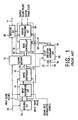
- the transmission signal processing circuit is for use in a synchronous digital multiplexing transmission device (not shown) and is supplied from a transmission line (not shown) with an input transmission signal 10 synchronized with input clock pulses.
- the input transmission signal comprises an input frame (namely, a transmission line frame) which is synchronized with an input frame pulse and which includes a TU.
- the transmission signal processing circuit is further supplied with output clock pulses and an output frame pulse from the synchronous digital multiplexing transmission device.
- the transmission signal processing circuit processes the input transmission signal into an output transmission signal 11 comprising an output frame (namely, a device frame) including the tributary unit by transferring the tributary unit from the input frame onto the output frame of the output transmission signal 11 with the output transmission signal 11 synchronized with the output clock pulses and with the output frame synchronized with the output frame pulse.
- an output transmission signal 11 comprising an output frame (namely, a device frame) including the tributary unit by transferring the tributary unit from the input frame onto the output frame of the output transmission signal 11 with the output transmission signal 11 synchronized with the output clock pulses and with the output frame synchronized with the output frame pulse.
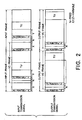
- the input transmission signal 10 of Fig. 1 is depicted along a first or top row.
- the input transmission signal includes an AU (administration unit) pointer which designates a location X of a leading edge of a VC (virtual container) frame in the input frame.
- the input transmission signal further includes a TU pointer in the input frame with a fixed interval N left between the leading edge of the VC frame and the TU pointer.
- the TU pointer designates another location Y of a leading edge of the TU in the input frame.
- An input pointer described in the preamble of the instant specification corresponds to the TU pointer which designates the location Y of the leading edge of the TU in the input frame.
- the output transmission signal 11 of Fig. 1 is depicted along a second or bottom row.
- the output transmission signal includes the AU pointer which designates the location 0 (zero) of the leading edge of the VC frame in the output frame.
- the output transmission signal further includes the TU pointer in the output frame with the fixed interval N left between the leading edge of the VC frame and the TU pointer.
- the TU pointer designates still another location Z of the leading edge of the TU in the output frame.
- An output pointer described in the preamble of the instant specification corresponds to the TU pointer which designates the location Z of the leading edge of the TU in the output frame.
- the transmission signal processing circuit transfers the TU from the input frame onto the output frame with the leading edge of the VC frame shifted so as to make the AU pointer of the output frame designate the location 0.
- the transmission signal processing circuit also carries out renewal of the TU pointer from the input pointer to the output pointer.
- the transmission signal processing circuit is therefore called a TU pointer processing circuit as described in the preamble of the instant specification.
- the TU of the input frame has one of a plurality of predetermined signal rates of the TU's of four sorts which are a TU-11, a TU-12, a TU-2, and a TU-3 and which are mentioned in the preamble of the instant specification. It will also be assumed that the transmission signal processing circuit of Fig. 1 should deal with the TU's of four sorts (namely, the TU-11, the TU-12, the TU-2, and the TU-3).
- the transmission signal processing circuit comprises a buffer memory 12 supplied with the input transmission signal 10.
- a deriving circuit 13 derives the input clock pulses and the input frame pulse from the input transmission signal 10.
- An input recognition circuit 14 is supplied with the input transmission signal 10 and with a plurality of signal rate information signals representative of the predetermined signal rates of the TU's of four sorts (namely, the TU-11, the TU-12, the TU-2, and the TU-3). Connected to the deriving circuit 13, the input recognition circuit 14 recognizes the TU of the input frame in response to the input clock pulses and the input frame pulse and with reference to the TU pointer of the input frame. The input recognition circuit 14 furthermore recognizes whether or not the TU of the input frame has a signal rate which corresponds to one of the predetermined signal rates represented by the signal rate information signals.
- the input recognition circuit 14 recognizes whether or not the TU of the input frame corresponds to one of the TU's of four sorts (namely, the TU-11, the TU-12, the TU-2, and the TU-3) with reference to the signal rate information signals.
- the input recognition circuit 14 recognizes that the TU of the input frame corresponds to one of the TU's of four sorts (namely, the TU-11, the TU-12, the TU-2, and the TU-3)
- the input recognition circuit 14 produces a location signal representative of a location of the TU in the input frame.
- a write controller 15 is connected to the deriving circuit 13 and the input recognition circuit 14.
- the write controller 15 controls writing of the TU of the input frame in the buffer memory 12 in response to the input clock pulses, the input frame pulse, and the location signal by supplying a write instruction signal 16 and a write address signal 17 to the buffer memory 12.
- the write controller 15 supplies the write instruction signal 16 and the write address signal 17 to the buffer memory 12 so that only the TU of the input frame is written in the buffer memory 12.
- a read controller 18 is supplied with the output clock pulses and the output frame pulse.
- the read controller 18 controls reading of the TU out of the buffer memory 12 in response to a stuff request signal 19 (which is either a positive stuff request signal 20 or a negative stuff request signal 21) by supplying a read address signal 23 and a read instruction signal 24 to the buffer memory 12.
- a stuff request signal 19 which is either a positive stuff request signal 20 or a negative stuff request signal 21
- the TU is read out of the buffer memory 12.
- a stuff execution judgement circuit 25 is given an input stuff threshold value 26 which is a combination of an input positive stuff threshold value 27 and an input negative stuff threshold value 28 which is greater than the input positive stuff threshold value 27.
- the stuff execution judgement circuit 25 judges whether or not a positive stuff operation should be executed by comparing a phase difference between the write address signal 17 and the read address signal 23 with the input positive stuff threshold value 27.
- the stuff execution judgement circuit 25 produces the positive stuff request signal 20 as the stuff request signal 19 when the stuff execution judgement circuit 25 judges that the positive stuff operation should be executed. More specifically, the stuff execution judgement circuit 25 produces the positive stuff request signal 20 when the phase difference is less than the input positive stuff threshold value 27. Responsive to the positive stuff request signal 20, the read controller 18 interrupts a reading operation to thereby increase the phase difference. As a result, a phase of an output signal of the buffer memory 12 becomes late.
- the stuff execution judgement circuit 25 furthermore judges whether or not a negative stuff operation should be executed by comparing the phase difference with the input negative stuff threshold value 28.
- the stuff execution judgement circuit 25 produces the negative stuff request signal 21 as the stuff request signal 19 when the stuff execution judgement circuit 25 judges that the negative stuff operation should be executed. More specifically, the stuff execution judgement circuit 25 produces the negative stuff request signal 21 when the phase difference is greater than the input negative stuff threshold value 28. Responsive to the negative stuff request signal 21, the read controller 18 carries out inverse control to decrease the phase difference.
- a pointer producing circuit 29 is supplied with the output clock pulses and the output frame pulse and supplied with the read address signal 23 and the read instruction signal 24 from the read controller 18. Further supplied with the locating signal from the input recognition circuit 14, the pointer producing circuit 29 produces the output pointer equivalent to the TU pointer which designates the location Z of the leading edge of the TU in the output frame of Fig. 2.
- An inserting circuit 30 is connected to the buffer memory 12 and the pointer producing circuit 29. The inserting circuit 30 inserts the output pointer in the output frame which includes the TU read out of the buffer memory 12. The inserting circuit 30 thereby produces the output transmission signal 11 which includes both the output pointer and the TU in the output frame.
- a combination of the pointer producing circuit 29 and the inserting circuit 30 is operable as an output transmission signal producing circuit. Supplied with the output clock pulses and the output frame pulse and connected to the buffer memory 12, the output transmission signal producing circuit produces the output transmission signal 11.
- the stuff execution judgement circuit 25 is given a constant input positive stuff threshold value 27 and a constant input negative stuff threshold value 28 no matter whether the TU of the input transmission signal 10 has any signal rate. That is, the input stuff threshold value 26 is constant or fixed for the TU's of four sorts (namely, the TU-11, the TU-12, the TU-2, and the TU-3). This results in an increase of a delay required from a write timing of the TU in the buffer memory 12 to a read timing of the TU under consideration out of the buffer memory 12 when the TU under consideration has a particular signal rate as mentioned above.
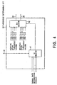
- the transmission signal processing circuit of Fig. 3 is similar to the transmission signal processing circuit of Fig. 1 expect for the following. That is, the input recognition circuit 14 of the transmission signal processing circuit of Fig. 3 further produces a sort signal 31 representative of a sort of the TU in the input frame.
- the transmission signal processing circuit of Fig. 3 further comprises a threshold determining circuit 32. Supplied with the signal rate information signals and connected to the input recognition circuit 14, the threshold determining circuit 32 determines in response to the sort signal 31 an optimum stuff threshold value 33 which is a combination of an optimum positive stuff threshold value 34 and an optimum negative stuff threshold value 35. The threshold determining circuit 32 thereby produces the optimum stuff threshold value 33 as the input stuff threshold value of the stuff execution judgement circuit 25.
- the threshold determining circuit 32 includes first and second selectors 41 and 42.
- the first selector 41 is given the signal rate information signals representative of the predetermined signal rates of the TU's of four sorts (namely, the TU-11, the TU-12, the TU-2, and the TU-3).
- the first selector 41 selects one of the signal rate information signals as a selected rate information signal.
- the above-mentioned one of the signal rate information signals corresponds to the sort of the TU that is represented by the sort signal 31.
- the second selector 42 is given a plurality of predetermined positive stuff threshold values in correspondence to the predetermined signal rates of the TU's of four sorts (namely, the TU-11, the TU-12, the TU-2, and the TU-3) and is also given a plurality of predetermined negative stuff threshold values in correspondence to the predetermined signal rates of the TU's of four sorts (namely, the TU-11, the TU-12, the TU-2, and the TU-3). That is, the second selector 42 is given the predetermined positive stuff threshold values for the TU-11, the TU-12, the TU-2, and the TU-3 and is also given the predetermined negative stuff threshold values for the TU-11, the TU-12, the TU-2, and the TU-3.
- the second selector 42 selects, as the optimum positive stuff threshold value 34 and the optimum negative stuff threshold value 35, one of the predetermined positive stuff threshold values for the TU-11, the TU-12, the TU-2, and the TU-3 and one of the predetermined negative stuff threshold values for the TU-11, the TU-12, the TU-2, and the TU-3.
- the above-mentioned one of the predetermined positive stuff threshold values and the above-mentioned one of the predetermined negative stuff threshold values correspond to the selected rate information signal produced by the first selector 41.
Landscapes
- Engineering & Computer Science (AREA)
- Computer Networks & Wireless Communication (AREA)
- Signal Processing (AREA)
- Computer Hardware Design (AREA)
- Time-Division Multiplex Systems (AREA)
- Synchronisation In Digital Transmission Systems (AREA)
Claims (4)
- Übertragungssignalverarbeitungsschaltung, die dazu geeignet ist, ein mit Eingangstaktimpulsen synchronisiertes Eingangsübertragungssignal (10) zu empfangen, wobei das Eingangsübertragungssignal einen mit einem Eingangsrahmenimpuls synchronisierten Eingangsrahmen und eine Tributary Unit aufweist, wobei die Übertragungssignalverarbeitungsschaltung ferner dazu geeignet ist, Ausgangstaktimpulse und einen Ausgangsrahmenimpuls zu empfangen, um das Eingangsübertragungssignal in ein Ausgangsübertragungssignal (11) zu verarbeiten, das einen Ausgangsrahmen aufweist, der die Tributary Unit aufweist, indem die Tributary Unit vom Eingangsrahmen zum Ausgangsrahmen des Ausgangsübertragungssignals übertragen wird, wobei das Ausgangsübertragungssignal mit den Ausgangstaktimpulsen synchronisiert ist und der Ausgangsrahmen mit dem Ausgangsrahmenimpuls synchronisiert ist;
wobei die Übertragungssignalverarbeitungsschaltung aufweist:dadurch gekennzeichnet, daßeine Ableitungs- oder Entnahmeschaltung (13) zum Entnehmen der Eingangstaktimpulse und des Eingangsrahmenimpulses vom Eingangsübertragungssignal;einen Speicher (12), der dazu geeignet ist, das Eingangsübertragungssignal zu empfangen;eine Erkennungsschaltung (14), die dazu geeignet ist, das Eingangsübertragungssignal zu empfangen und die mit der Entnahmeschaltung verbunden ist, um die Tributary Unit des Eingangsrahmens in Antwort auf die Eingangstaktimpulse und den Eingangsrahmenimpuls zu erkennen, um ein die Position der Tributary Unit im Eingangsrahmen darstellendes Positionssignal zu erzeugen;einen mit der Entnahmeschaltung und der Erkennungsschaltung verbundenen Schreibcontroller (15) zum Steuern des Schreibvorgangs zum Schreiben der Tributary Unit des Eingangsrahmens in Antwort auf die Eingangstaktimpulse; den Eingangsrahmenimpuls und das Positionssignal in den Speicher durch Zuführen eines Schreibadressensignals (17) zum Speicher;einen Lesecontroller (18), der dazu geeignet ist, die Ausgangstaktimpulse und den Ausgangsrahmenimpuls zu empfangen, um den Lesevorgang zum Auslesen der Tributary Unit aus dem Speicher in Antwort auf ein Stopfanforderungssignal (19) durch Zuführen eines Leseadressensignals (23) zum Speicher zu steuern;eine Stopfverarbeitungsentscheidungsschaltung (25), der ein Eingangs-Stopfschwellenwert zugeführt wird, und die mit dem Schreibcontroller und dem Lesecontroller verbunden ist, um durch Vergleichen einer Differenz zwischen dem Schreibadressensignal und dem Leseadressensignal mit dem Eingangs-Stopfschwellenwert zu entscheiden, ob eine Stopfverarbeitung ausgeführt werden sollte oder nicht, wobei die Stopfverarbeitungsentscheidungsschaltung das Stopfanforderungssignal erzeugt, wenn die Stopfverarbeitungsentscheidungsschaltung entscheidet, daß die Stopfverarbeitung ausgeführt werden sollte; undeine Ausgangs-Übertragungssignalerzeugungsschaltung (29, 30), der die Ausgangstaktimpulse und der Ausgangsrahmenimpuls zugeführt werden, und die mit dem Speicher verbunden ist, um das Ausgangsübertragungssignal zu erzeugen;
die Erkennungsschaltung dazu geeignet ist, ein den Typ der Tributary Unit im Eingangsrahmen darstellendes Typsignal (31) zu erzeugen; und
die Übertragungssignalverarbeitungsschaltung ferner aufweist:eine mit der Erkennungsschaltung verbundene Schwellenwertbestimmungsschaltung (32) zum Bestimmen eines optimalen Stopfschwellenwertes (33) in Antwort auf das Typsignal, um den optimalen Stopfschwellenwert als den Eingangs-Stopfschwellenwert zu erzeugen. - Übertragungssignalverarbeitungsschaltung nach Anspruch 1, wobei die Tributary Unit eine von mehreren vorgegebenen Signalraten im Eingangsrahmen aufweist, und wobei die Schwellenwertbestimmungsschaltung aufweist:einen ersten Selektor (41), dem mehrere Signalrateninformationssignale zugeführt werden, die die vorgegebenen Signalraten darstellen, und der mit der Erkennungsschaltung verbunden ist, um eines der Signalrateninformationssignale als ein ausgewähltes Rateninformationssignal auszuwählen, wobei das eine der Signalrateninformationssignale dem durch das Typsignal dargestellten Typ der Tributary Unit entspricht; undeinen zweiten Selektor (42), dem mehrere vorgegebene Stopfschwellenwerte gemäß den vorgegebenen Signalraten zugeführt werden, und der mit dem ersten Selektor verbunden ist, um einen der vorgegebenen Stopfschwellenwerte als den optimalen Stopfschwellenwert auszuwählen, wobei der eine der vorgegebenen Stopfschwellenwerte dem ausgewählten Rateninformationssignal entspricht.
- Übertragungssignalverarbeitungsschaltung nach Anspruch 1, wobei der Stopfverarbeitungsentscheidungsschaltung als Eingangs-Stopfschwellenwert ein positiver Eingangs-Stopfschwellenwert und ein negativer Eingangs-Stopfschwellenwert zugeführt wird, wobei die Stopfverarbeitungsentscheidungsschaltung durch Vergleichen der Differenz mit dem positiven Eingangs-Stopfschwellenwert entscheidet, ob eine positive Stopfverarbeitung ausgeführt werden sollte oder nicht, wobei die Stopfverarbeitungsentscheidungsschaltung ein positives Stopfanforderungssignal (20) als Stopfanforderungssignal erzeugt, wenn die Stopfverarbeitungsentscheidungsschaltung entscheidet, daß die positive Stopfverarbeitung ausgeführt werden sollte, und wobei die Stopfverarbeitungsentscheidungsschaltung durch Vergleichen der Differenz mit dem negativen Eingangs-Stopfschwellenwert entscheidet, ob eine negative Stopfverarbeitung ausgeführt werden sollte oder nicht, wobei die Stopfverarbeitungsentscheidungsschaltung ein negatives Stopfanforderungssignal (21) als Stopfanforderungssignal erzeugt, wenn die Stopfverarbeitungsentscheidungsschaltung entscheidet, daß die negative Stopfverarbeitung ausgeführt werden sollte;
wobei die Schwellenwertbestimmungsschaltung dazu geeignet ist, in Antwort auf das Typsignal einen optimalen positiven Stopfschwellenwert (34) und einen optimalen negativen Stopfschwellenwert (35) als optimalen Stopfschwellenwert zu bestimmen, um den optimalen positiven Stopfschwellenwert und den optimalen negativen Stopfschwellenwert als den positiven Eingangs-Stopfschwellenwert bzw. den negativen Eingangs-Stopfschwellenwert zu erzeugen. - Übertragungssignalverarbeitungsschaltung nach Anspruch 3, wobei die Tributary Unit eine von mehreren vorgegebenen Signalraten im Eingangsrahmen aufweist, und wobei die Schwellenwertbestimmungseinheit aufweist:einen ersten Selektor (41), dem mehrere die vorgegebenen Signalraten darstellende Signalrateninformationssignale zugeführt werden, und der mit der Erkennungsschaltung verbunden ist, um eines der Signalrateninformationssignale als ein ausgewähltes Rateninformationssignal auszuwählen, wobei das eine der Signalrateninformationssignale dem durch das Typsignal dargestellten Typ der Tributary Unit entspricht; undeinen zweiten Selektor (42), dem mehrere den vorgegebenen Signalraten entsprechende, vorgegebene positive Stopfschwellenwerte und mehrere den vorgegebenen Signalraten entsprechende, vorgegebene negative Stopfschwellenwerte zugeführt werden, und der mit dem ersten Selektor verbunden ist, um einen der vorgegebenen positiven Stopfschwellenwerte als den optimalen positiven Stopfschwellenwert auszuwählen und einen der vorgegebenen negativen Stopfschwellenwerte als den optimalen negativen Stopfschwellenwert auszuwählen, wobei der eine der vorgegebenen positiven Stopfschwellenwerte und der eine der vorgegebenen negativen Stopfschwellenwerte dem ausgewählten Rateninformationssignal entspricht.
Applications Claiming Priority (3)
| Application Number | Priority Date | Filing Date | Title |
|---|---|---|---|
| JP6326305A JP2616731B2 (ja) | 1994-12-27 | 1994-12-27 | 伝送信号処理回路 |
| JP32630594 | 1994-12-27 | ||
| JP326305/94 | 1994-12-27 |
Publications (3)
| Publication Number | Publication Date |
|---|---|
| EP0720320A2 EP0720320A2 (de) | 1996-07-03 |
| EP0720320A3 EP0720320A3 (de) | 1998-07-29 |
| EP0720320B1 true EP0720320B1 (de) | 2004-03-17 |
Family
ID=18186286
Family Applications (1)
| Application Number | Title | Priority Date | Filing Date |
|---|---|---|---|
| EP95120568A Expired - Lifetime EP0720320B1 (de) | 1994-12-27 | 1995-12-27 | Übertragungssignalverarbeitungsschaltung, die einen optimalen Stopfschwellwert bestimmen kann entsprechend der Untersystemeinheit des Eingangssignales |
Country Status (6)
| Country | Link |
|---|---|
| US (1) | US5642357A (de) |
| EP (1) | EP0720320B1 (de) |
| JP (1) | JP2616731B2 (de) |
| CA (1) | CA2166139C (de) |
| DE (1) | DE69532705T2 (de) |
| MY (1) | MY111859A (de) |
Families Citing this family (10)
| Publication number | Priority date | Publication date | Assignee | Title |
|---|---|---|---|---|
| US5841762A (en) * | 1996-03-29 | 1998-11-24 | British Telecommunications Public Limited Company | Monitoring a synchronous digital hierarchy transmission path |
| DE19732943A1 (de) * | 1997-07-31 | 1999-02-04 | Alsthom Cge Alcatel | Verfahren und Komponente zum Ausgleich von Frequenz- und Phasenschwankungen |
| US6229863B1 (en) | 1998-11-02 | 2001-05-08 | Adc Telecommunications, Inc. | Reducing waiting time jitter |
| JP2003078497A (ja) * | 2001-09-04 | 2003-03-14 | Fujitsu Ltd | 伝送装置 |
| JP3970581B2 (ja) | 2001-11-09 | 2007-09-05 | 富士通株式会社 | 伝送装置および伝送システム |
| US7839887B1 (en) * | 2003-10-16 | 2010-11-23 | Network Equipment Technologies, Inc. | Method and system for providing frame rate adaption |
| JP2006270792A (ja) * | 2005-03-25 | 2006-10-05 | Fujitsu Ltd | フレーム伝送方法及び装置 |
| US7839885B2 (en) * | 2005-04-25 | 2010-11-23 | Lsi Corporation | Connection memory for tributary time-space switches |
| JP4729049B2 (ja) * | 2005-12-22 | 2011-07-20 | 日本電信電話株式会社 | 光送信器 |
| US8681917B2 (en) | 2010-03-31 | 2014-03-25 | Andrew Llc | Synchronous transfer of streaming data in a distributed antenna system |
Family Cites Families (8)
| Publication number | Priority date | Publication date | Assignee | Title |
|---|---|---|---|---|
| CA1262173A (en) * | 1986-05-29 | 1989-10-03 | James Angus Mceachern | Synchronization of asynchronous data signals |
| JP2782731B2 (ja) * | 1988-09-19 | 1998-08-06 | 日本電気株式会社 | 同期多重化網の回線乗換え方式及び回線乗換えに用いられる演算回路 |
| LU87714A1 (de) * | 1989-11-29 | 1990-07-24 | Siemens Ag | Verfahren zum uebertragen eines digitalen breitbandsignals in einer untersystemeinheitenkette ueber ein netz einer synchron-digital-multiplexhierarchie |
| DE4013317A1 (de) * | 1990-04-26 | 1990-08-23 | Ant Nachrichtentech | Stopfverfahren zur reduktion des wartezeitjitters und anordnung zur durchfuehrung des verfahrens |
| US5263057A (en) * | 1990-05-09 | 1993-11-16 | Ant Nachrichtentechnik Gmbh | Method of reducing waiting time jitter |
| US5276688A (en) * | 1990-06-09 | 1994-01-04 | U.S. Philips Corporation | Circuit arrangement for bit rate adjustment |
| US5331641A (en) * | 1990-07-27 | 1994-07-19 | Transwitch Corp. | Methods and apparatus for retiming and realignment of STS-1 signals into STS-3 type signal |
| DE4108429A1 (de) * | 1991-03-15 | 1992-09-17 | Philips Patentverwaltung | Uebertragungssystem fuer die digitale synchrone hierarchie |
-
1994
- 1994-12-27 JP JP6326305A patent/JP2616731B2/ja not_active Expired - Fee Related
-
1995
- 1995-12-27 US US08/578,079 patent/US5642357A/en not_active Expired - Lifetime
- 1995-12-27 DE DE69532705T patent/DE69532705T2/de not_active Expired - Lifetime
- 1995-12-27 EP EP95120568A patent/EP0720320B1/de not_active Expired - Lifetime
- 1995-12-27 CA CA002166139A patent/CA2166139C/en not_active Expired - Fee Related
- 1995-12-27 MY MYPI95004115A patent/MY111859A/en unknown
Also Published As
| Publication number | Publication date |
|---|---|
| MY111859A (en) | 2001-01-31 |
| EP0720320A3 (de) | 1998-07-29 |
| JP2616731B2 (ja) | 1997-06-04 |
| CA2166139C (en) | 1999-02-23 |
| CA2166139A1 (en) | 1996-06-28 |
| DE69532705T2 (de) | 2004-08-05 |
| US5642357A (en) | 1997-06-24 |
| JPH08186556A (ja) | 1996-07-16 |
| DE69532705D1 (de) | 2004-04-22 |
| EP0720320A2 (de) | 1996-07-03 |
Similar Documents
| Publication | Publication Date | Title |
|---|---|---|
| US5210745A (en) | Frame restructuring interface for digital bit streams multiplexed by time-division multiplexing digital tributaries with different bit rates | |
| EP0459686B1 (de) | Synchronisierung eines digitalen Signals mit einer elastischen Speicherung | |
| US5359605A (en) | Circuit arrangement for adjusting the bit rates of two signals | |
| EP0529012B1 (de) | Verfahren und anordnung für datensynchronisierung | |
| US4543652A (en) | Time-division switching unit | |
| EP0720320B1 (de) | Übertragungssignalverarbeitungsschaltung, die einen optimalen Stopfschwellwert bestimmen kann entsprechend der Untersystemeinheit des Eingangssignales | |
| EP0559649A1 (de) | Verfahren und mittel zum transfer einer datennutzlast von einem ersten sonet-signal zu einem sonet-signal mit unterschiedlicher frequenz | |
| US5563877A (en) | Telecommunication network node | |
| US4920547A (en) | Stuff synchronization circuit | |
| US5515362A (en) | Digital signal transmission apparatus | |
| EP0584636B1 (de) | Phasendetektor für elastischen Speicherung | |
| US7639673B2 (en) | Method and apparatus for SDH/SONET frame alignment | |
| EP0699363B1 (de) | Verfahren und vorrichtung zum bestimmen einer stopfentscheidung in einem knoten eines synchronen digitalen nachrichtenübertragungssystems (sdh) | |
| JPH0621929A (ja) | 伝送装置および等化回路装置 | |
| US5357515A (en) | Non-interruption transmission line switching system in a duplex transmission network | |
| US5923669A (en) | Adaptive boundary buffers | |
| WO1994003023A1 (en) | Method for implementing time switching and a time switch | |
| EP1073226B1 (de) | Verfahren zur Abbildung von Übertragungsbändern in Zeitrahmen in Telekommunikationsnetzwerken und entsprechende Schaltung | |
| JP3198675B2 (ja) | データレート変換装置 | |
| KR0168921B1 (ko) | 동기식 전송시스템에서 시험액세스를 위한 24x3교차 스위치 회로 | |
| JP3010634B2 (ja) | フレーム同期多重処理方式 | |
| JPH04322525A (ja) | 同期ディジタルハイアラーキにおけるポインタ値発生方法 | |
| HK1011821B (en) | Method for implementing time switching and a time switch | |
| JPH0670384A (ja) | クロスコネクト装置 |
Legal Events
| Date | Code | Title | Description |
|---|---|---|---|
| PUAI | Public reference made under article 153(3) epc to a published international application that has entered the european phase |
Free format text: ORIGINAL CODE: 0009012 |
|
| AK | Designated contracting states |
Kind code of ref document: A2 Designated state(s): DE FR SE |
|
| PUAL | Search report despatched |
Free format text: ORIGINAL CODE: 0009013 |
|
| AK | Designated contracting states |
Kind code of ref document: A3 Designated state(s): DE FR SE |
|
| 17P | Request for examination filed |
Effective date: 19980623 |
|
| 17Q | First examination report despatched |
Effective date: 20021106 |
|
| GRAP | Despatch of communication of intention to grant a patent |
Free format text: ORIGINAL CODE: EPIDOSNIGR1 |
|
| GRAS | Grant fee paid |
Free format text: ORIGINAL CODE: EPIDOSNIGR3 |
|
| GRAA | (expected) grant |
Free format text: ORIGINAL CODE: 0009210 |
|
| AK | Designated contracting states |
Kind code of ref document: B1 Designated state(s): DE FR SE |
|
| REG | Reference to a national code |
Ref country code: SE Ref legal event code: TRGR |
|
| REF | Corresponds to: |
Ref document number: 69532705 Country of ref document: DE Date of ref document: 20040422 Kind code of ref document: P |
|
| ET | Fr: translation filed | ||
| PLBE | No opposition filed within time limit |
Free format text: ORIGINAL CODE: 0009261 |
|
| STAA | Information on the status of an ep patent application or granted ep patent |
Free format text: STATUS: NO OPPOSITION FILED WITHIN TIME LIMIT |
|
| 26N | No opposition filed |
Effective date: 20041220 |
|
| PGFP | Annual fee paid to national office [announced via postgrant information from national office to epo] |
Ref country code: SE Payment date: 20081205 Year of fee payment: 14 |
|
| EUG | Se: european patent has lapsed | ||
| PG25 | Lapsed in a contracting state [announced via postgrant information from national office to epo] |
Ref country code: SE Free format text: LAPSE BECAUSE OF NON-PAYMENT OF DUE FEES Effective date: 20091228 |
|
| PGFP | Annual fee paid to national office [announced via postgrant information from national office to epo] |
Ref country code: DE Payment date: 20131224 Year of fee payment: 19 |
|
| PGFP | Annual fee paid to national office [announced via postgrant information from national office to epo] |
Ref country code: FR Payment date: 20131209 Year of fee payment: 19 |
|
| REG | Reference to a national code |
Ref country code: DE Ref legal event code: R119 Ref document number: 69532705 Country of ref document: DE |
|
| REG | Reference to a national code |
Ref country code: FR Ref legal event code: ST Effective date: 20150831 |
|
| PG25 | Lapsed in a contracting state [announced via postgrant information from national office to epo] |
Ref country code: DE Free format text: LAPSE BECAUSE OF NON-PAYMENT OF DUE FEES Effective date: 20150701 |
|
| PG25 | Lapsed in a contracting state [announced via postgrant information from national office to epo] |
Ref country code: FR Free format text: LAPSE BECAUSE OF NON-PAYMENT OF DUE FEES Effective date: 20141231 |