EP0714535B1 - Skalares unterbrechungs-rückquittierungssystem - Google Patents
Skalares unterbrechungs-rückquittierungssystem Download PDFInfo
- Publication number
- EP0714535B1 EP0714535B1 EP94922449A EP94922449A EP0714535B1 EP 0714535 B1 EP0714535 B1 EP 0714535B1 EP 94922449 A EP94922449 A EP 94922449A EP 94922449 A EP94922449 A EP 94922449A EP 0714535 B1 EP0714535 B1 EP 0714535B1
- Authority
- EP
- European Patent Office
- Prior art keywords
- count
- processed
- unprocessed
- response
- detected
- Prior art date
- Legal status (The legal status is an assumption and is not a legal conclusion. Google has not performed a legal analysis and makes no representation as to the accuracy of the status listed.)
- Expired - Lifetime
Links
Images





Classifications
-
- G—PHYSICS
- G06—COMPUTING OR CALCULATING; COUNTING
- G06F—ELECTRIC DIGITAL DATA PROCESSING
- G06F13/00—Interconnection of, or transfer of information or other signals between, memories, input/output devices or central processing units
- G06F13/14—Handling requests for interconnection or transfer
- G06F13/20—Handling requests for interconnection or transfer for access to input/output bus
- G06F13/24—Handling requests for interconnection or transfer for access to input/output bus using interrupt
Definitions
- the present invention relates to data processing systems and, in particular, to an interrupt-acknowledgement circuit that generates a single interrupt signal when a plurality of events are detected and that allows a host device to process all of the detected events without delayed processing, spurious interrupts, or additional overhead.
- a simple interrupt-acknowledgement protocol can be utilized to define the communications between the peripheral device and the host device.
- the peripheral device typically detects a single event, generates a single interrupt signal in response to the detected event, and then ignores subsequent events until the interrupt signal is acknowledged by the host device (i.e., the host device modifies a register on the peripheral device).
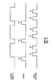
- FIG. 1 shows a timing diagram which illustrates the operation of the host device and the peripheral device under a simple interrupt-acknowledgement protocol.
- the detection of a series of events by the peripheral device is represented in FIG. 1 by a series of event pulses 10 where the falling edge 12 of each event pulse 10 represents the detection of a complete event.
- the peripheral device generates the rising edge 14 of an interrupt signal V 1 in response to the falling edge 12 of a detected event.
- each event 10 by the host device is represented in FIG. I by a series of processing pulses 16.
- the host device begins processing each event 10 a leading delay time T1 after the rising edge 14 of the interrupt signal V I is generated.
- the host device completes the processing of the event 10 and then generates an acknowledgement signal V A which is received by the peripheral device a trailing delay time T2 after the event has been processed, thereby causing the interrupt signal V I to be deasserted.
- the leading and trailing delay times T1 and T2 can represent, for example, the time required to communicate with the peripheral device via a bus.
- a peripheral device which, as stated above, ignores intervening events can potentially lose all of the data packets transmitted while the interrupt signal is asserted.
- the peripheral device typically detects a burst of packets and then generates a single interrupt signal in response to the first packet detected.
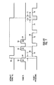
- FIG. 2 shows a timing diagram which illustrates the operation of the host device and the network interface device under a process-then-acknowledge many-to-one protocol.
- the detection of a burst of packets by the network interface device is represented in FIG. 2 as a series of packet pulses 20 where the falling edge 22 represents the detection of a first complete packet.
- the network interface device generates the rising edge 24 of an interrupt signal V II in response to the falling edge 22 of the first detected packet.
- each packet 20 by the host device is represented in FIG. 2 by a series of packet processing pulses 26.
- the host device processes all of the packets 20 detected by the network interface device and then acknowledges the interrupt signal V II the trailing delay time T2 after the last packet is processed.
- a delayed notification condition occurs when the host device completes the processing of all the packets detected by the network interface device at approximately the same time that the network interface device detects a new packet.
- FIG. 3 shows a timing diagram which illustrates a delayed notification from the network interface device to the host device under a process-then-acknowledge many-to-one protocol.
- the burst of packets 20 are represented by a first packet 28, a second packet 30, and a third packet 32.
- the processing of the first packet 28 is represented by a first packet pulse 34 while the processing of the second packet 30 is represented by a second packet pulse 36.
- the host device completes the processing of the second packet 30 and during the trailing delay time T2, while the host device is transmitting an acknowledgement signal to the network interface device, the network interface device detects the third packet 32.
- the presence of the third packet 32 goes undetected because the interrupt signal V II is still asserted during the trailing delay time T2.
- the third packet will remain stored in the network interface device until the next packet is detected and the interrupt signal V II is reasserted.
- FIG. 4 shows a timing diagram which illustrates the host device rechecking a network interface device.
- the burst of packets 20 includes a fourth packet 38 while the processing of the fourth packet is represented by a packet processing pulse 40.
- the series of packet processing pulses includes a rechecking pulse 42.
- the host device rechecks the network interface device, as shown by the rechecking pulse 42, to insure that no packet goes undetected.
- FIG. 5 shows a timing diagram which illustrates the host device rechecking the network interface device, as represented by the rechecking pulse 42, after a single packet 44 has been processed, as represented by a processing pulse 46.
- the host device is able to process each packet detected by the network interface device before a subsequent packet is detected, the additional overhead is present with each packet processed.
- an acknowledge-then-process many-to-one protocol which acknowledges the interrupt signal before any packets are processed, can also be utilized.
- the network interface device detects a packet and then generates the interrupt signal in response.
- FIG. 6 shows a timing diagram which illustrates the operation of the host device and the peripheral device under an acknowledge-then-process many-to-one protocol.
- the detection of a series of packets is represented in FIG. 6 as a series of packet pulses 52 where the falling edge 54 represents the detection of a complete packet.
- the network interface device generates the rising edge 56 of the interrupt signal V II in response to the falling edge 54 of a completely detected packet.
- each packet 52 by the host device is represented in FIG. 6 by a series of packet processing pulses 58. As shown in FIG. 6, the host device acknowledges the interrupt signal V II and then processes a detected packet.
- a spurious interrupt condition occurs when the network interface device generates an interrupt signal after the host device has acknowledged the interrupt signal but before the host device completes the processing of all of the detected packets.
- the spurious interrupt causes the host device to attempt to process packets which do not exist.
- FIG. 7 shows a timing diagram which illustrates the generation of a spurious interrupt signal.
- the burst of packets 52 are represented by a first packet 62, a second packet 64, and a third packet 66.
- the processing of the packets are correspondingly represented by a first packet processing pulse 70, a second packet processing pulse 72, and a third packet processing pulse 74.
- the spurious interrupt signal is represented by a spurious packet processing pulse 76.
- the network interface device generates the rising edge 56 of the interrupt signal V II in response to the falling edge 54 of the first detected packet 62.
- the host device acknowledges the interrupt signal V II and then begins processing the first packet 62.
- the network interface device detects the second and the third packets 64 and 66, and reasserts the interrupt signal V II .
- the host device processes all three of the packets 62, 64, and 66 detected by the network interface device. Since the interrupt signal V II was reasserted when the second packet 64 was detected, the host device reacknowledges the interrupt signal, as shown by the spurious packet processing pulse 76, and then attempts to process packets which do not exist.
- FIG. 8 shows a timing diagram which illustrates the effect of acknowledging the interrupt signal prior to processing each packet. As shown in FIG. 8, when an acknowledgement signal V AA is generated with the processing of each packet, three acknowledgements are generated when only one is required.
- an interrupt-acknowledgement circuit that generates a single interrupt signal when a plurality of events are detected and that allows a host device to process all of the detected events without delayed processing, the generation of spurious signals, or the use of additional overhead such as redundant checks or acknowledgements.
- the present invention provides a scalar interrupt-acknowledgement system which utilizes counters to count both the number of unprocessed events and the number of processed events, and to both assert and deassert an interrupt signal in response to the values held by the counters.
- a scalar interrupt-acknowledgement system which utilizes counters to count both the number of unprocessed events and the number of processed events, and to both assert and deassert an interrupt signal in response to the values held by the counters.
- a peripheral device includes a detector and an unprocessed event counter.
- the detector detects one or more events and generates a first increment signal in response to each detected event.
- the unprocessed event counter counts the number of unprocessed events by incrementing an unprocessed count in response to each first increment signal and by decrementing the unprocessed count by the value of a processed count each time an externally-generated processed count word is received where each externally-generated processed count word defines the value of the processed count.
- the unprocessed event counter also asserts an interrupt signal when the unprocessed count indicates that an event remains unprocessed, such as when the unprocessed count is greater than zero, and deasserts the interrupt signals when the unprocessed count indicates that all of the detected events have been processed, such as when the unprocessed count is equal to zero.
- a host device includes a processor and a processed event counter.
- the processor processes the events detected by an external detector, generates a second increment signal in response to the processing of each detected event, and produces a transmit signal each time a number of the detected events are processed.
- the processed event counter counts the number of processed events by incrementing a processed count value in response to each second increment signal, transmits a processed count word which represents the processed count in response to the transmit signal, and resets the processed count in response to the transmission of each processed count word.
- the unprocessed event counter can include, for example, a memory that stores the processed count, as transmitted by each processed count word, and the unprocessed count.
- An adder/subtractor adds a count to the unprocessed count in response to each first increment signal, and subtracts the processed count from the unprocessed count each time the unprocessed count word is received.
- a comparator asserts the interrupt signal when the unprocessed count indicates that detected events remain unprocessed, and deasserts the interrupt signal when the unprocessed count indicates that all detected events have been processed.
- the processor may, for example, generate the second increment signal before or after each event is processed.
- FIG. 1 is a timing diagram illustrating the operation of the host device and the peripheral device under a simple interrupt-acknowledgement protocol.
- FIG. 2 is a timing diagram illustrating the operation of the host device and the network interface device under a process-then-acknowledge many-to-one protocol.
- FIG. 3 is a timing diagram illustrating a delayed notification from the network interface device to the host device under a process-then-acknowledge many-to-one protocol.
- FIG. 4 is a timing diagram illustrating the host device rechecking a network interface device.
- FIG. 5 is a timing diagram illustrating the host device rechecking the network interface device, as represented by the rechecking pulse 42, after a single packet 44 has been processed, as represented by a processing pulse 46.
- FIG. 6 is a timing diagram illustrating the operation of the host device and the peripheral device under an acknowledge-then-process many-to-one protocol.
- FIG. 7 is a timing diagram illustrating the generation of a spurious interrupt signal.
- FIG. 8 is a timing diagram illustrating the effect of acknowledging the interrupt signal prior to processing each packet.
- FIG. 9 is a block diagram illustrating a network interface device and a host device which implement a scalar interrupt-acknowledgement system in accordance with the present invention.
- FIG. 10 is a block diagram illustrating an embodiment of detected packet counter 118.
- FIG. 11 is a block diagram illustrating how the bits of RAM 210 which correspond to the unprocessed count can be connected to comparator 214 to detect the zero and non-zero condition when RAM 210 is written to or read from.
- FIG. 9 shows a block diagram of a network interface device 110 and a host device 112 that implement a scalar interrupt-acknowledgement system in accordance with the present invention.
- the scalar interrupt-acknowledgement system utilizes counter circuitry to count both the number of detected packets and the number of processed packets, and to both assert and deassert an interrupt signal in response to the values held by the counter circuitry.
- network interface device 110 includes a packet detector 114 and a detected packet counter 116.
- Network interface device 110 detects data packets DP transmitted to network interface device 110 across an external bus 118, generates an increment signal V INCR1 in response to each detected data packet DP, stores the detected data packets DP for retransmission, and retransmits the stored data packets as received data packets RDP in response to a request signal V R .
- the detected packet counter 116 counts the number of unprocessed packets by incrementing an unprocessed count in response to each increment signal V INCR1 , and by decrementing the unprocessed count by the value of a processed count each time an externally-generatedprocessed count word PCW is received where each externally-generated processed count word PCW defines the value of the processed count.
- Detected packet counter 116 also asserts an interrupt signal V INT when the unprocessed count is greater than zero, and deasserts the interrupt signal V INT when the unprocessed count is equal to zero. Alternately, other counting schemes can also be used.
- host device 112 includes a packet processor 120 and a processed packet counter 122.
- Processor 120 generates the request signal V R in response to the interrupt signal V INT , receives and processes the received data packets RDP retransmitted by packet detector 114, and generates an increment signal V INCR2 in response to the processing of each detected packet.
- packet processor 120 can generate the increment signal V INCR2 either before or after the processing of each packet.
- the packet processor 120 also generates a transmit signal V T when the processing of a number of the received data packets RDP has been completed. For example, the packet processor 120 could generate the transmit signal V T following the processing of every nth received data packet RDP or when the processing of all the received data packets RDP have been processed.
- processed packet counter 122 counts the number of processed packets by incrementing a processed count in response to each increment signal V INCR2 , transmits the processed count as the processed count word PCW in response to the transmit signal V T , and resets the processed count in response to the transmission of each processed count word PCW.
- network interface device 110 and host device 112 are able to accurately track the number of remaining or unprocessed packets.
- network interface device 110 and host device 112 transmit and receive the processed count word PCW, the interrupt signal V INT , the request signal V R , and the received data packets RDP across a shared bus.
- network interface device 110 asserts the interrupt signal V INT after the first packet is detected and counted, and then continues to count each subsequently detected packet.
- Host device 112 asynchronously processes and counts each packet detected by network interface device 110.
- host device 112 To acknowledge the interrupt signal V INT , host device 112 writes the processed count back to network interface device 110 as the processed count word PCW. Network interface device 110 then subtracts the processed count from the unprocessed count to determine whether the interrupt signal V INT should be deasserted. Thus, when the transmit signal is generated after all of the packets have been processed, host device 112 need make only a single access across the shared bus to acknowledge the interrupt signal V INT . Since both network interface device 110 and host device 112 maintain a count of the number of packets detected and processed, the delayed notification and spurious interrupt conditions cannot arise.
- each bus master may retain the bus up to 7.8 microseconds. With five bus masters, it can take up to 39 microseconds before the host device can access the network interface device. Since the scalar interrupt-acknowledgement system maintains a count of both the unprocessed and processed packets, less bus time is required.
- FIG. 10 shows a block diagram of an embodiment of detected packet counter 116.
- detected packet counter 116 can be implemented using a random access memory (RAM) 210, an adder/subtractor 212, and a comparator 214.
- RAM 210 stores the processed count, as transmitted by the processed count word PCW, and the unprocessed count.
- Adder/subtractor 212 adds a count to the unprocessed count in response to each increment signal V INCR1 and subtracts the processed count from the unprocessed count each time the processed count word PCW is received.
- Comparator 214 asserts the interrupt signal V INT when the unprocessed count is greater than zero and deasserts the interrupt signal V INT when the unprocessed count is equal to zero.
- FIG. 11 shows a block diagram which illustrates how the bits of RAM 210 which correspond to the unprocessed count can be connected to comparator 214 to detect the zero and non-zero condition when RAM 210 is written to or read from.
Landscapes
- Engineering & Computer Science (AREA)
- Theoretical Computer Science (AREA)
- Physics & Mathematics (AREA)
- General Engineering & Computer Science (AREA)
- General Physics & Mathematics (AREA)
- Bus Control (AREA)
Claims (9)
- Scalare Unterbrechungs-Bestätigungs-Schaltung zur Erzeugung eines einzelnen Unterbrechungssignals, wenn eine Anzahl von Ereignissen erfaßt wird, wobei die Schaltung aufweist:einen Detektor (114), der ein oder mehrere Ereignisse detektiert und ein erstes Inkrementsignal in Abhängigkeit von jedem detektierten Ereignis erzeugt,einen Prozessor (120), der die durch den Detektor detektierten Ereignisse verarbeitet, ein zweites Inkrementsignal in Abhängigkeit von der Verarbeitung jedes detektierten Ereignisses erzeugt und ein Übermittlungssignal erzeugt, wenn die detektierten Ereignisse verarbeitet werden,einen Zähler (122) für verarbeitete Ereignisse, der die Anzahl der verarbeiteten Ereignisse durch Inkrementieren einer Verarbeitungszählung in Abhängigkeit von jedem zweiten Inkrementsignal zählt, in Abhängigkeit von dem Übermittlungssignal ein Verarbeitungszählungswort übermittelt, das die Verarbeitungszählung wiedergibt, und die Verarbeitungszählung in Abhängigkeit von der Übermittlung jedes Verarbeitungszählungswortes zurückstellt, undeinen Zähler (116) für unverarbeitete Ereignisse, der die Anzahl von unverarbeiteten Ereignisse durch Inkrementieren eines Unverarbeitungszählers in Abhängigkeit von jedem ersten Inkrementsignal und durch Dekrementieren der Unverarbeitungszählung durch die Verarbeitungszählung, die durch jedes Verarbeitungszählungswort wiedergegeben ist, in Abhängigkeit von einem Empfang jedes Verarbeitungszählungswortes zählt, ein Unterbrechungssignal aktiviert, wenn die Unverarbeitungszählung anzeigt, daß ein Ereignis unverarbeitet verblieben ist, und das Unterbrechungssignal deaktiviert, wenn die Unverarbeitungszählung anzeigt, daß alle erfaßten Ereignisse verarbeitet sind.
- Schaltung nach Anspruch 1, wobei der Prozessor (120) das zweite Inkrementsignal erzeugt, nachdem jedes Ereignis verarbeitet wurde.
- Schaltung nach Anspruch 1, wobei der Prozessor (120) das zweite Inkrementsignal erzeugt, bevor jedes Ereignis verarbeitet ist.
- Schaltung nach einem der vorstehenden Ansprüche, wobei der Unverarbeitungsereigniszähler (116) aufweist:einen Speicher (210), der die Verarbeitungszählung wie durch das Verarbeitungszählungswort übermittelt speichert und die Unverarbeitungszählung,einen Addierer/Subtrahierer (212), der eine Zählung zu der Unverarbeitungszählung in Abhängigkeit von jedem ersten Inkrementsignal addiert und die Verarbeitungszählung von der Unverarbeitungszählung in Abhängigkeit von dem Empfang des Unverarbeitungszählungswortes subtrahiert, undeinen Vergleicher (214), der das Unterbrechungssignal aktiviert, wenn die Unverarbeitungszählung anzeigt, daß detektierte Ereignisse unverarbeitet sind, und das Unterbrechungssignal deaktiviert, wenn die Unverarbeitungszählung anzeigt, daß alle detektierten Ereignisse verarbeitet sind.
- Schaltung nach Anspruch 4, wobei der Vergleicher (214) das Unterbrechungssignal aktiviert, wenn die Unverarbeitungszählung größer als 0 ist, und das Unterbrechungssignal deaktiviert, wenn die Unverarbeitungszählung gleich 0 ist.
- Schaltung nach einem der vorstehenden Ansprüche, wobei der Prozessor (120) das Übermittlungssignal während der Verarbeitung der detektierten Ereignisse erzeugt.
- Schaltung nach einem der vorstehenden Ansprüche, wobei jedes Ereignis eine Datenpaket ist.
- Verfahren zum Erzeugen eines einzelnen Unterbrechungssignals, wenn eine Anzahl von Ereignissen detektiert wird, wobei das Verfahren die Schritte aufweist:Detektieren von einem oder mehreren Ereignissen und Erzeugen eines ersten Inkrementsignals in Abhängigkeit von jedem detektierten Ereignis,Verarbeiten der detektierten Ereignisse, Erzeugen eines zweiten Inkrementsignals in Abhängigkeit von der Verarbeitung jedes detektierten Ereignisses und Erzeugen eines Übermittlungssignals, wenn die detektierten Ereignisse verarbeitet werden,Zählen der Anzahl der verarbeiteten Ereignisse durch Inkrementieren einer Verarbeitungszählung in Abhängigkeit von jedem zweiten Inkrementsignal, Übermitteln eines Verarbeitungszählungswortes, das die Verarbeitungszählung wiedergibt, in Abhängigkeit von dem Übermittlungssignal und Rückstellen der Verarbeitungszählung in Abhängigkeit von der Übermittlung jedes Verarbeitungszählungswortes, undZählen der Anzahl von unverarbeiteten Ereignissen durch Inkrementieren einer Unverarbeitungszählung in Abhängigkeit von jedem ersten Inkrementsignal und durch Dekrementieren der Unverarbeitungszählung durch die Verarbeitungszählung, die durch jedes Verarbeitungszählungswort wiedergegeben wird, in Abhängigkeit von einem Empfang jedes Verarbeitungszählungswortes, Aktivieren eines Unterbrechungssignals, wenn die Unverarbeitungszählung anzeigt, daß ein Ereignis unverarbeitet geblieben ist, und Deaktivieren des Unterbrechungssignals, wenn die Unverarbeitungszählung anzeigt, daß alle erfaßten Ereignisse verarbeitet sind.
- Verfahren nach Anspruch 8, wobei jedes Ereignis ein Datenpaket ist.
Applications Claiming Priority (3)
| Application Number | Priority Date | Filing Date | Title |
|---|---|---|---|
| US08/097,438 US5913071A (en) | 1993-07-26 | 1993-07-26 | Scalar interrupt-acknowledgement system that responds to a plurality of events with a single interrupt signal |
| US97438 | 1993-07-26 | ||
| PCT/US1994/007117 WO1995003584A1 (en) | 1993-07-26 | 1994-06-24 | A scalar interrupt-acknowledgement system |
Publications (2)
| Publication Number | Publication Date |
|---|---|
| EP0714535A1 EP0714535A1 (de) | 1996-06-05 |
| EP0714535B1 true EP0714535B1 (de) | 1999-01-20 |
Family
ID=22263346
Family Applications (1)
| Application Number | Title | Priority Date | Filing Date |
|---|---|---|---|
| EP94922449A Expired - Lifetime EP0714535B1 (de) | 1993-07-26 | 1994-06-24 | Skalares unterbrechungs-rückquittierungssystem |
Country Status (6)
| Country | Link |
|---|---|
| US (1) | US5913071A (de) |
| EP (1) | EP0714535B1 (de) |
| JP (1) | JPH09500992A (de) |
| KR (1) | KR100302891B1 (de) |
| DE (1) | DE69416138T2 (de) |
| WO (1) | WO1995003584A1 (de) |
Families Citing this family (7)
| Publication number | Priority date | Publication date | Assignee | Title |
|---|---|---|---|---|
| US5659758A (en) * | 1995-07-07 | 1997-08-19 | Sun Microsystems, Inc. | Interrupt modular for receiving bursty high speed network traffic |
| US6012115A (en) * | 1997-07-28 | 2000-01-04 | Vlsi Technology, Inc. | Method and system for accurate temporal determination of real-time events within a universal serial bus system |
| US6615305B1 (en) * | 1998-08-27 | 2003-09-02 | Intel Corporation | Interrupt pacing in data transfer unit |
| US6195725B1 (en) * | 1998-12-14 | 2001-02-27 | Intel Corporation | Dynamically varying interrupt bundle size |
| DE10052834B4 (de) * | 2000-10-24 | 2019-09-19 | Leica Biosystems Nussloch Gmbh | Verfahren zur Behandlung von Objekten |
| US7953906B2 (en) * | 2007-02-20 | 2011-05-31 | Ati Technologies Ulc | Multiple interrupt handling method, devices and software |
| US9304955B2 (en) * | 2012-12-18 | 2016-04-05 | Advanced Micro Devices, Inc. | Techniques for identifying and handling processor interrupts |
Family Cites Families (6)
| Publication number | Priority date | Publication date | Assignee | Title |
|---|---|---|---|---|
| JPS4995548A (de) * | 1973-01-12 | 1974-09-10 | ||
| FR2470412B1 (fr) * | 1979-11-19 | 1986-10-03 | Bull Sa | Procede et dispositif de comptabilisation et de gestion des evenements asynchrones emis par des appareils peripheriques dans un systeme de traitement de donnees |
| JPS57196357A (en) * | 1981-05-29 | 1982-12-02 | Toshiba Corp | Data processor |
| US4851987A (en) * | 1986-01-17 | 1989-07-25 | International Business Machines Corporation | System for reducing processor power consumption by stopping processor clock supply if a desired event does not occur |
| US5313622A (en) * | 1990-08-16 | 1994-05-17 | National Instruments | Timing apparatus and method for generating instruction signals |
| EP0477448B1 (de) * | 1990-09-28 | 1995-07-12 | Hewlett-Packard Company | Netzüberwachungssystem und -vorrichtung |
-
1993
- 1993-07-26 US US08/097,438 patent/US5913071A/en not_active Expired - Lifetime
-
1994
- 1994-06-24 KR KR1019960700405A patent/KR100302891B1/ko not_active Expired - Fee Related
- 1994-06-24 JP JP7505155A patent/JPH09500992A/ja not_active Ceased
- 1994-06-24 DE DE69416138T patent/DE69416138T2/de not_active Expired - Fee Related
- 1994-06-24 EP EP94922449A patent/EP0714535B1/de not_active Expired - Lifetime
- 1994-06-24 WO PCT/US1994/007117 patent/WO1995003584A1/en not_active Ceased
Also Published As
| Publication number | Publication date |
|---|---|
| EP0714535A1 (de) | 1996-06-05 |
| KR100302891B1 (ko) | 2001-11-22 |
| JPH09500992A (ja) | 1997-01-28 |
| US5913071A (en) | 1999-06-15 |
| DE69416138D1 (de) | 1999-03-04 |
| WO1995003584A1 (en) | 1995-02-02 |
| KR960704272A (ko) | 1996-08-31 |
| DE69416138T2 (de) | 1999-07-22 |
Similar Documents
| Publication | Publication Date | Title |
|---|---|---|
| US4785396A (en) | Push-pull serial bus coupled to a plurality of devices each having collision detection circuit and arbitration circuit | |
| US5802048A (en) | Method and apparatus for accelerating arbitration in a serial bus by detection of acknowledge packets | |
| US4070648A (en) | Computer to computer communication system | |
| US20040236875A1 (en) | Computer for dynamically determining interrupt delay | |
| US6205153B1 (en) | System and method for improving CSMA/CD network performance during collisions | |
| US5913071A (en) | Scalar interrupt-acknowledgement system that responds to a plurality of events with a single interrupt signal | |
| US4621323A (en) | Message transmission circuitry | |
| US20080031386A1 (en) | Method and device for robust signal detection in wireless communications | |
| US6130619A (en) | Monitoring circuit for a communication device | |
| EP0490002B1 (de) | Flagzählerschaltung | |
| JP2834062B2 (ja) | 情報処理システム | |
| JP2844656B2 (ja) | 割込制御回路 | |
| SU1520530A1 (ru) | Устройство дл сопр жени ЭВМ с каналом св зи | |
| JPH0465577B2 (de) | ||
| JP3060660B2 (ja) | 端末装置の送信制御方式 | |
| CN119254568A (zh) | 一种用于异常时序处理的音频数据传输总线接口 | |
| CN118592018A (zh) | 检测装置及检测方法 | |
| CN120216417A (zh) | 一种数据处理方法、装置、芯片、芯片系统和电子设备 | |
| US7124182B2 (en) | Method for real-time detection of which units are present on an arcnet | |
| JPH0723049A (ja) | 通信端末装置 | |
| JPH0136740B2 (de) | ||
| JPH06350673A (ja) | プロトコル処理装置 | |
| JPS6221426B2 (de) | ||
| JPH0546501A (ja) | シリアルインターフエイス方式 | |
| EP0465206A2 (de) | Geteiltes Arbitrierungsgerät verwendbar für einen tauben Knotenpunkt |
Legal Events
| Date | Code | Title | Description |
|---|---|---|---|
| PUAI | Public reference made under article 153(3) epc to a published international application that has entered the european phase |
Free format text: ORIGINAL CODE: 0009012 |
|
| 17P | Request for examination filed |
Effective date: 19960125 |
|
| AK | Designated contracting states |
Kind code of ref document: A1 Designated state(s): DE FR GB |
|
| 17Q | First examination report despatched |
Effective date: 19970102 |
|
| GRAG | Despatch of communication of intention to grant |
Free format text: ORIGINAL CODE: EPIDOS AGRA |
|
| GRAG | Despatch of communication of intention to grant |
Free format text: ORIGINAL CODE: EPIDOS AGRA |
|
| GRAH | Despatch of communication of intention to grant a patent |
Free format text: ORIGINAL CODE: EPIDOS IGRA |
|
| GRAH | Despatch of communication of intention to grant a patent |
Free format text: ORIGINAL CODE: EPIDOS IGRA |
|
| GRAA | (expected) grant |
Free format text: ORIGINAL CODE: 0009210 |
|
| AK | Designated contracting states |
Kind code of ref document: B1 Designated state(s): DE FR GB |
|
| PG25 | Lapsed in a contracting state [announced via postgrant information from national office to epo] |
Ref country code: FR Free format text: LAPSE BECAUSE OF FAILURE TO SUBMIT A TRANSLATION OF THE DESCRIPTION OR TO PAY THE FEE WITHIN THE PRESCRIBED TIME-LIMIT Effective date: 19990120 |
|
| REF | Corresponds to: |
Ref document number: 69416138 Country of ref document: DE Date of ref document: 19990304 |
|
| EN | Fr: translation not filed | ||
| PG25 | Lapsed in a contracting state [announced via postgrant information from national office to epo] |
Ref country code: GB Free format text: LAPSE BECAUSE OF NON-PAYMENT OF DUE FEES Effective date: 19990624 |
|
| PLBE | No opposition filed within time limit |
Free format text: ORIGINAL CODE: 0009261 |
|
| STAA | Information on the status of an ep patent application or granted ep patent |
Free format text: STATUS: NO OPPOSITION FILED WITHIN TIME LIMIT |
|
| 26N | No opposition filed | ||
| GBPC | Gb: european patent ceased through non-payment of renewal fee |
Effective date: 19990624 |
|
| PGFP | Annual fee paid to national office [announced via postgrant information from national office to epo] |
Ref country code: DE Payment date: 20080731 Year of fee payment: 15 |
|
| PG25 | Lapsed in a contracting state [announced via postgrant information from national office to epo] |
Ref country code: DE Free format text: LAPSE BECAUSE OF NON-PAYMENT OF DUE FEES Effective date: 20100101 |