EP0708918B1 - Vorrichtung zur spektralanalyse unter einer mehrzahl von winkeln - Google Patents
Vorrichtung zur spektralanalyse unter einer mehrzahl von winkeln Download PDFInfo
- Publication number
- EP0708918B1 EP0708918B1 EP94921955A EP94921955A EP0708918B1 EP 0708918 B1 EP0708918 B1 EP 0708918B1 EP 94921955 A EP94921955 A EP 94921955A EP 94921955 A EP94921955 A EP 94921955A EP 0708918 B1 EP0708918 B1 EP 0708918B1
- Authority
- EP
- European Patent Office
- Prior art keywords
- detector
- sample
- incidence
- elements
- light
- Prior art date
- Legal status (The legal status is an assumption and is not a legal conclusion. Google has not performed a legal analysis and makes no representation as to the accuracy of the status listed.)
- Expired - Lifetime
Links
Images


Classifications
-
- G—PHYSICS
- G01—MEASURING; TESTING
- G01B—MEASURING LENGTH, THICKNESS OR SIMILAR LINEAR DIMENSIONS; MEASURING ANGLES; MEASURING AREAS; MEASURING IRREGULARITIES OF SURFACES OR CONTOURS
- G01B11/00—Measuring arrangements characterised by the use of optical techniques
- G01B11/02—Measuring arrangements characterised by the use of optical techniques for measuring length, width or thickness
- G01B11/06—Measuring arrangements characterised by the use of optical techniques for measuring length, width or thickness for measuring thickness ; e.g. of sheet material
- G01B11/0616—Measuring arrangements characterised by the use of optical techniques for measuring length, width or thickness for measuring thickness ; e.g. of sheet material of coating
- G01B11/0641—Measuring arrangements characterised by the use of optical techniques for measuring length, width or thickness for measuring thickness ; e.g. of sheet material of coating with measurement of polarization
-
- G—PHYSICS
- G01—MEASURING; TESTING
- G01N—INVESTIGATING OR ANALYSING MATERIALS BY DETERMINING THEIR CHEMICAL OR PHYSICAL PROPERTIES
- G01N21/00—Investigating or analysing materials by the use of optical means, i.e. using sub-millimetre waves, infrared, visible or ultraviolet light
- G01N21/17—Systems in which incident light is modified in accordance with the properties of the material investigated
- G01N21/21—Polarisation-affecting properties
- G01N21/211—Ellipsometry
Definitions
- This invention relates to an apparatus for evaluating a sample.
- the preferred devices rely on non-contact, optical measurement techniques.
- a probe beam is directed to the sample, and a particular parameter of the reflected probe beam is measured.
- the intensity of the reflected probe beam will vary due to the variation in interference effects created at the interface between the thin film and the substrate.
- the thickness of the thin film will have an effect on the change in polarization state which occurs when the probe beam is reflected off the sample surface.
- a spectrophotometer is designed to provide interferometric type measurements at various wavelengths.
- Another approach for gaining additional accuracy is to take measurements at a number of different angles of incidence of the probe beam.
- the probe beam was generated by a laser having an output that was substantially diffraction limited allowing focusing to a spot size on the order of one micron in diameter. This approach provides high spatial resolution permitting analysis of extremely small regions on the sample.
- a means is provided for sequentially or simultaneously selecting a plurality of individual wavelengths.
- the means can include various combinations of filters, gratings or prisms.
- the need to provide wavelength selective elements adds to the cost and complexity of the apparatus as well as requiring moving parts. More significantly, the need to take sequential measurements slows the operation of the device. Therefore, it would be desirable to be able to obtain simultaneous measurements not only at different angles, but at different wavelengths as well.
- US-A-5 166 752 to Dogr, which describes a simultaneous multiple angle of incidence ellipsometer.
- One embodiment of the device includes a polychromatic light source.
- Figure 5 of US-A-5 166 752 illustrates a method by which it is suggested that simultaneous measurements can be made at both multiple angles of incidence and at multiple wavelengths. This approach includes providing a dispersing element for spreading out the beam as a function of wavelength.
- a collimated beam of polychromatic light is brought to a point focus on a sample surface by a converging lens the optical axis of which makes an acute angle with the normal to the surface at the focal point, so that in a plane of incidence containing the optical axis of the lens, a range of angles of incidence is provided.
- the reflected light is gathered by another converging lens placed so as to collimate the divergent reflected beam.
- the collimated beam is then directed through the dispersing element to a photodetector having a two dimensional array of individual detector elements.
- the array is oriented so that each column measures light from only a narrow band of wavelengths at a plurality of angles of incidence.
- the columns are disposed parallel to the plane of incidence containing the optical axes of the two lenses.
- each row is arranged to obtain measurements at a single angle of incidence at various wavelengths.
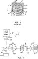
- Figure 1 illustrates a two dimensional photodetector array 10 of the type proposed by Dogr.
- the array includes a plurality of rows 6 and columns 8 of detector elements. Superimposed on top of the array are the foot prints of two different probe beams (2 and 4) having different wavelengths.
- the pattern of the probe beams (2,4) would be of the type created using a dispersing element to spatially separate the wavelengths in a polychromatic beam.
- the dispersing element is oriented in a manner to separate light of different wavelengths along a vertical axis so that the detector elements across each row 6 measure light as a function of angle of incidence.
- Arrow A in Figure 1 is aligned with the row of photodetector elements associated with the central diameter of beam 2.
- the left and right-hand detector elements 14 and 16 will correspond to the maximum and minimum angles of incidence in the beam.
- the spread of angles of incidence is on the order of 128 degrees.
- the detector elements 14 and 16 at the radially outermost points on the beam will measure rays having angles of incidence of +64 degrees and -64 degrees.
- the light falling on element 18 is not limited to light associated with the wavelength of beam 2. Rather, light from beam 4 of an adjacent wavelength falls on element 18 as well. Having light of different wavelengths fall on individual detector elements will complicate the wavelength dependent analysis of the sample. More significantly, the light falling on element 18 from beam 4 corresponds to a substantially different angle of incidence than the light from beam 2. This difference can be appreciated by comparing the radial distance between the center of beam 2 and element 18 (R1) with the radial distance between the center of beam 4 and element 18 (R2). As can be seen, the radial distance R2 is significantly greater than the radial distance R1.
- the angle of incidence is directly related to the radial position of the rays within the beam, it can be seen that the angle of incidence for the light ray of the wavelength of beam 4 at element 18 is larger than the angle of incidence for the ray associated with beam 2 at element 18. In the illustrated example, the angle of incidence of the ray for beam 4 at element 18 would be on the order of 46 degrees as compared to the 27 degrees for beam 2.
- Preferred embodiments of the invention provide: an improved method for simultaneously measuring both angle and wavelength information contained in a reflected probe beam;
- a preferred embodiment of the invention allows for easily varying the area on the sample over which measurements are taken.
- a spot size on the order of one micron can be obtained using a fast lens.
- a white light source such tight focusing is not possible and a much wider area is illuminated.
- the minimum focused spot size which could be achieved with a white light source would be on the order of 150 microns in diameter.
- This preferred embodiment provides a system wherein the selected measurement region can be less than the minimum focused spot size diameter, and a device wherein the size of the measurement region can be easily changed without moving or replacing the lens elements.
- the preferred embodiment takes the form of a simultaneous multiple angle of incidence measurement device, particularly suited for evaluating thin films on semiconductors.
- a simultaneous multiple angle of incidence measurement device particularly suited for evaluating thin films on semiconductors.
- the advances discussed herein can be used on both interferometric and ellipsometric devices.
- Both aspects relate to the use of white light sources with simultaneous multiple angle of incidence measurement devices.
- the use of a white light source allows measurements to be taken at multiple wavelengths.
- One problem associated with a non-coherent white light source is that the focused spot size tends to be larger than that which can be achieved using a coherent laser source.
- the area of measurement can be reduced using a variable image filter located in the path of the reflected beam and prior to the detector.
- the variable image filter consists of a combination of a relay lens and an aperture plate.
- the aperture plate is located in the focal plane of the lens.
- the relay lens projects an image of the beam as it exists on the sample surface onto the aperture plate.
- variable image filter described was utilized to limit spurious reflections returning from outside the focused laser beam spot from reaching the detector.
- the preferred embodiment of the present invention differs from that prior disclosure in that the variable image filter herein is used to image a region smaller than the focused white light spot. More significantly, in the preferred embodiment disclosed herein, the variable image filter is provided with a plurality of aperture plates allowing the size of the imaged region to be easily selected by the operator without having to change and/or reposition the lens elements.
- the method disclosed herein for improving simultaneous multiple wavelength measurements in devices which also simultaneously measure light at multiple angles of incidence is applicable to either interferometric or ellipsometric devices.
- the preferred measurement device will include a polychromatic light source for generating a probe beam of radiation, and a microscope objective used to focus the probe beam on the sample in a manner to create a spread of angles of incidence and a detector provided to analyze the reflected probe beam.
- the detector will measure the intensity of the beam.
- the detector components will determine the change in polarization state which occurs when the beam interacts with the sample.
- the detector will measure various rays as a function of their radial position within the reflected probe beam to provide specific data on different angles of incidence with respect to the sample surface.
- a wavelength dispersion element is located in the path of the reflected probe beam.
- the dispersion element functions to angularly spread the beam as a function of wavelength.
- the detector includes a two dimensional array of elements, wherein each row of elements measures the full angle of incidence information for a different central wavelength.
- a spatial filter is located in the path of the reflected probe beam, prior to the dispersion element.
- the spatial filter includes a narrow rectangular aperture aligned along a diameter of the beam.
- the aperture should be oriented to be perpendicular to the plane in which the dispersion element angularly spreads the light.
- the dimensions of the aperture are selected to transmit a narrow cross-section of the beam that when imaged on the detector will correspond to the width of one row of detector elements.
- the aperture should transmit allow only about ten percent of the total cross-section of the beam.
- the narrow aperture substantially reduces the amount of overlap between beams of different wavelengths. Any overlap which occurs is limited to wavelengths which are close, minimizing the adverse affect on wavelength dependent calculations. Moreover, the adverse impact of overlapping wavelength information is almost fully eliminated because there is no overlap of different angle of incidence information. More specifically, since the slit filter is arranged so that the only light passing through is along a single beam diameter, the radial distance from the center of the transmitted rectangular cross-section to a given detector element illuminated by that beam will be essentially the same for any wavelength. If the radial distance is the same for all wavelengths, then the angle of incidence of the light rays striking that detector element are the same as well. Therefore, the detector assembly provides isolation for simultaneous multiple angles of incidence measurements while simultaneously measuring multiple wavelengths.
- the probe beam light is linearly polarized and a spherical objective is used to focus the light on the sample surface.
- the spherical objective lens creates light having orthogonally related S and P-polarization states.
- the aperture in the filter is aligned with one of the axes so that either the S or P-polarization components can be isolated.
- Figure 1 is an illustration of an approach for producing simultaneous multiple angle and multiple wavelength measurements not embodying the invention.
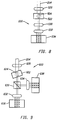
- Figure 2 is a schematic diagram of an optical measurement device incorporating the concepts of the subject invention.
- Figure 3 is an illustration depicting the appearance of the probe beam after it passes through the filter 60 of Figure 2.
- Figure 4 is an illustration depicting the appearance of the probe beams associated with two different wavelengths after the probe beam has passed through the dispersion element 62 of Figure 2.
- FIG 5 is an illustration similar to Figure 4 except that the wavelengths shown are closer together such that the separation between the probe beams is less.
- Figure 6 is a schematic diagram of a device wherein simultaneous multiple angle of incidence measurements can be made at a plurality of selected wavelengths.
- Figure 7 is a schematic diagram of a replacement detection assembly suitable for simultaneous measurement at multiple angles of incidence and multiple wavelengths which can isolate pure polarization states of the probe beam in the device of Figure 6.
- Figure 8 is a schematic diagram of a further replacement detection assembly suitable for deriving ellipsometric parameters based on the simultaneous measurement of both multiple angle of incidence and multiple wavelength information for use in the device of Figure 6.
- Figure 9 is a schematic diagram of another replacement detection assembly suitable for simultaneous measurement of integrated ellipsometric data at multiple wavelengths as well as specific angle of incidence information for use in the device of Figure 6.
- Figure 2 there is illustrated a system 30 for performing optical measurements in accordance with the subject invention.
- Figure 2 includes a light source 32 for generating polychromatic or white light with multiple wavelength components.
- the non-coherent output 34 is focused onto the surface of the sample 36 via a spherical microscope objective lens 40.
- the sample can be mounted on a movable stage 42 to allow the probe beam to be scanned over the sample.
- the probe beam 34 is directed normal to the sample surface and lens 40 has a high numerical aperture, on the order of 0.90.
- This high numerical aperture creates a large spread of angles of incidence on the surface of the sample 36.
- the angles of incidence can be traced within the reflected beam and simultaneously measured at the detector.
- the center ray corresponds to the central angle of incidence.
- the variation in the angle of incidence from the central angles varies in proportion to the increase in the radial position of the ray within the beam.
- the location of any ray in the reflected probe beam corresponds to the sine of the angle of incidence.
- the filter 50 consists of a relay lens 52 and a plate 54.
- Plate 54 is located in the focal plane of relay lens 52 and includes an aligned aperture 56.
- the relay lens projects a magnified image of the surface of the sample into the plane of plate 54.
- the extent of magnification is given by the ratio of the focal length of lens 52 divided by the focal length of lens 40. A typical magnification would be about 60.
- the aperture 56 is dimensioned so that it only transmits a portion of the relayed sample image.
- the amount of the image that is transmitted is defined by the size of the aperture divided by the magnification of the image.
- the non-coherent light source can be focused down to a spot size of about 150 microns in diameter.
- image spots on the order of a micron can be achieved.
- the diameter of the aperture would be 60 microns for a magnification of 60. It should be understood, however, that as the image of the spot is reduced, the energy reaching the detector is also reduced making measurement more difficult. Therefore, if larger image sizes are acceptable, (which is the case when high speed, average measurements are desired) more accurate results can be obtained with a larger image size.
- the reflected beam is then passed to the detection system.
- the detection system includes a filter 60, a dispersion element 62 and a detector 64. Suitable devices which could be used for detector 64 can be a two-dimensional photodiode array or a CCD camera.
- the prior art has suggested an approach which included the dispersion element and a two dimensional detector array.
- the dispersion element functioned to angularly spread the beam as a function of wavelength.
- Optical devices which are suitable for the dispersion element include prisms, gratings and holographic plates. By spreading the beam, it is possible to separately measure the intensity of the light rays as a function of wavelength.
- Filter 60 includes an aperture 72 configured to transmit only a portion of reflected beam 54.
- aperture 72 is in the form of an elongated slit which is positioned along a diameter of the beam and is located in the relay image plane of the exit pupil of the objective lens 40.
- lens 52 also serves to create this relay image.
- Aperture 72 is oriented in a manner to be perpendicular to the direction in which the dispersion element 62 angularly spreads the light.
- the dimensions of the slit 72 are selected so that the image transmitted to the detector will be on the order of the dimensions of a row of detector elements.
- the slit should be oriented in either the S or P-planes of polarization.
- Figure 3 illustrates the appearance of the beam just after it has passed through the aperture 72. As can be seen, only an elongated rectangular segment 74 is transmitted. The circular outline of the beam which has been blocked by filter 60 is shown in dotted line 76. Because the filter 60 is located in the relay image plane of the exit pupil of lens 40, the transmitted strip will include rays corresponding to all of the angles of incidence created by lens 40. In the preferred embodiment, point 78 will correspond to zero degrees, point 80 will correspond to 64 degrees and point 82 will correspond to 27 degrees.
- FIG 4 illustrates the beam 34 after it has passed through the dispersion element 62.
- Beams 86 and 88 represent two different wavelengths. The difference in the wavelengths is intended to be the same as the two beams illustrated in Figure 1.
- Each wavelength illustrated in Figure 4 includes a central rectangular transmitted segment 90, 92 carrying all of the angle of incidence information. As can be seen, for these two exemplary wavelengths, even though the circular beam foot prints would overlap, the transmitted segments do not, so there is no blurring of wavelength information for wavelengths having any significant difference. Thus, the row of detector elements aligned with segment 90 will provide full angle of incidence of information with no blurring of data from a second, disparate wavelength.
- Figure 5 illustrates the situation with beams 98 and 102 representing two, relatively closely spaced wavelengths. Where the two wavelengths are close, the dispersion element will provide only limited separation.
- the filter 60 of the subject invention substantially eliminates any measurement problems caused by the minimal overlap. More specifically, the aperture 72 in filter 60 is designed to transmit rays only along a single radial direction. Thus, the distance from the center of the beam to any given detector element will be substantially the same for each wavelength. Since this radial distance is the same, the angle of incidence of the rays falling on a given detector element will be the same for any wavelength.
- FIG. 5 This result can be seen in Figure 5 taking detector element 106 as an example.
- the aperture 72 in filter 60 limits the transmission to two elongated segments 108 and 110 for beams 98 and 102 respectively.
- the radial distances between the center of each beam and the detector element 106 are shown as R3 and R4. As can be seen, these two radial distances are essentially the same, so that the angle of incidence of the rays striking the detector element 106 are the same.
- the dispersion element 62 may cause the pattern of the beam to spread in a rectangular fashion.
- suitable additional optical elements such as a cylindrical lens 120 to recollimate the beam into a square format.
- any row of detector elements will cover the full angle of incidence measurements at a central wavelength for the either pure S or P-polarization state.
- One approach for deriving both S and P-information would be to take a second measurement after filter 60 and the dispersion element 62 have been rotated by ninety degrees as indicated by arrow B in Figure 2. In this orientation, the remaining pure polarization state information could be detected. If it was desired to measure both polarization states simultaneously, a beam splitter could be inserted in the path of the reflected beam prior to the filter 60 to redirect a portion of the beam along another path. The other path would then be provided with a separate filter, dispersion element and array detector. The separate filter and dispersion element would be oriented orthogonally with respect to the filter and dispersion elements along the main path. This arrangement is illustrated in Figure 7, discussed below.
- the filter 60 of the subject invention has a further advantage when attempting to measure light of pure S or P-polarization.
- an individual detector element will receive light from rays having different angles of incidence.
- the light from beam 4 is along a radial direction different from the radial direction of beam 2, it will also include a different combination of S and P-polarization states. If the row of elements designated by arrow A in Figure 1 were oriented such that it was receiving pure polarization state light from beam 2, the prior art measurement would be further degraded because the light from beam 4 would contain a blend of S and P-polarization information.
- the filter of the subject invention overcomes this problem as well.
- the aperture 72 of filter 60 should be aligned with one of the two polarization states. In that case, the only light which will be transmitted will be either S or P-polarized. Any light of unwanted or a mixed polarization state will be blocked.
- the computational advantages associated with using pure polarized light can be maintained while simultaneously measuring information at different wavelengths.
- the subject inventions can be utilized with either interferometric or ellipsometric devices.
- the main elements in Figure 2 represent an interferometric device wherein the intensity variations of the reflected light rays are monitored. Details of the type of analysis which can be performed with this data are set forth in U.S. Patent No. 4,999,014.
- additional elements For operation as an ellipsometer, additional elements must be provided for determining the change in polarization state of the beam which occurs upon reflection off of the sample.
- these additional elements would include the polarizer 122 and an analyzing section 132 (shown in phantom line).
- the polarizing and analyzing sections will include polarizing elements which can be rotated about the propagation axis of the beam. By knowing the relative azimuthal positions of these rotatable elements in conjunction with the intensity of measurements of detector 64, the change in polarization state of the rays in the beam can be determined.
- a discussion of simultaneous multiple angle of incidence ellipsometric analyses is set forth in U.S. Patent No. 5,042,951.
- Figure 2 illustrates both the improved variable image filter 50 and the detection system for simultaneous multiple angle of incidence and wavelength measurements, these two developments could be used separately. This independence can be appreciated with reference to Figure 6 which illustrates one preferred form of an optical measurement system using a white light source and a multiple aperture variable image filter.
- Figure 6 illustrates some of the additional elements which would be desirable in an simultaneous multiple angle of incidence interferometric measurement device 200.
- the device in Figure 6 uses a non-coherent light source 210 and a variable image filter 212.
- the device of Figure 6 does not include a detection system suitable for simultaneous measurement at multiple wavelengths. The latter feature is disclosed as an alternative in Figure 7.
- source 210 should be a bright, polychromatic or white light source such as a tungsten-halogen lamp.
- the light 214 from source 210 is then passed through one of a plurality of narrow band filters 220 for selecting one of a plurality of different wavelengths.
- the light is then passed through an on/off shutter 224 to polarizing beam splitter 226 for creating linearly polarized light.
- lens 230 which relays an image of the source onto the pupil of spherical microscope objective lens 232.
- lens 232 is arranged to tightly focus the beam normal to the surface of the sample 233 to create a large spread of angles of incidence.
- the lens also functions to create light with substantial components of S and P-polarized light.
- One axis will contain predominantly S-polarized light while the orthogonal axis will contain predominantly P-polarized light.
- the polarization states will be mixed.
- Detector 236 monitors the fluctuations in the output power of source 210 so that the measurements can be normalized.
- filter 212 includes a relay lens 254 which projects an image of the surface sample into the plane of plate 256.
- the filter includes a plurality of interchangeable plates each having a different size apertures 258. By this arrangement, the operator can select the size of the image field to be projected onto the principle detectors 260 and 262.
- the plates 256 may be mounted on a rotatable wheel (not shown). The desired aperture can be positioned in the beam path by adjusting the rotational angle of the wheel.
- each detector 260, 262 consists of a one dimensional linear array of photodetector elements. One array is oriented to provide full angle of incidence information for S-polarized light. The other array is oriented perpendicular to the first array and will provide full angle of incidence information for P-polarized light.
- simultaneous multiple angles of incidence information can be generated at a plurality of wavelengths in a sequential manner. This information will allow for an interferometric evaluation of thin film samples.
- the processor will evaluate the sample based on the simultaneous angular dependent intensity measurements made by the detectors. These intensity measurements are a function of the interference effects created by the interaction of the probe beam with the surface of the thin film and the interface between the thin film and the sample. These simultaneous angle of incidence measurements will be repeated for each of a plurality of different wavelengths selected by filters 220.
- two detectors each having a linear area of detector elements are utilized.
- a single detector head could be used having two orthogonally disposed linear arrays. The latter type of detector head is described in U.S. Patent No. 4,999,014.
- a full two dimensional array of the type shown in Figure 2 could be used.
- detector elements can also be used.
- a detector arrangement designed to measure different wavelengths simultaneously may be employed in which the use of the narrow band filters 220 can be eliminated.
- a portion of the light passing through filter 212 is picked off by a splitter 271 and directed to full power detector 272.
- measurement ambiguities from the multiple angle of incidence measurements can be resolved using an additional full beam power measurement.
- plates 256 are made reflective and redirect, to a camera 274, that portion of the image which is larger than the associated aperture 258 in plate 256.
- the image received by the camera 274 will have a central dark spot corresponding to that portion of the light transmitted by the aperture 258.
- a lens 276 is provided to image the sample surface onto the camera.
- the white light measurement system is combined with the elements for a laser detection system as described in U.S. Patent Nos. 4,999,014 and 5,181,080, assigned to the same assignee as herein and incorporated by reference.
- a laser diode 240 is used to generate a linearly polarized probe beam 280.
- the wavelength of the output is preferably on the order of 650 to 820nm.
- the probe beam 280 is passed through an on/off shutter 282 to a beam splitter 284. A portion of the beam passes through splitter 284 and falls on incident power detector 286 for monitoring fluctuations in the output of the laser diode.
- the remainder of the beam is redirected down through beam splitter 250 to lens 232 and focused on the sample 233. Since the beam from the laser is monochromatic and reasonably coherent, it can be focused down to a spot size on the order of one micron by lens 232. A portion of the reflected beam is redirected by splitter 290 to an autofocus system used to maintain the focus of the lens 232 and onto sample 233. In the assignees present commercial devices wherein this type of autofocus system is used, the lens focus spacing can be maintained to less than one hundredth of a micron.
- the autofocus system includes servo mechanisms 292 for varying the vertical position of the lens 232.
- the servo is driven by an analog detection loop which determines if the lens 232 is properly focusing the probe beam.
- the detection loop includes the reflected light which is focused by a lens 294 through a chopper wheel 296 located in the focal plane of lens 294. The light passing the chopper wheel 296 falls on a split-cell photodetector 298. If the lens 232 is out of focus, there will be a phase difference in the light striking the two sides of the split cell 298 which is detected by a phase detector 302. The phase difference is used as an input to an amplifier 304 which in turn drives the servo 292.
- This approach to autofocusing is known as the automated Foucault knife edge focus method.
- both specific multiple angle of incidence information as well as a signal which represents an integration of the intensity of all rays having different angles of incidence is measured for the laser probe beam 280.
- a portion of the returning reflected probe laser beam is redirected by splitter 250 to splitter 234.
- Splitter 234 redirects the probe laser beam downwardly towards detector arrays 260 and 262.
- the detector arrays 260, 262 are used to measure light from both the white light source 210 and the laser 240, the measurements should be taken sequentially, with only one source emitting radiation at a time. Sequential operation is achieved using shutters 224 and 282. Since the power output of the two sources will be different, it will be necessary to adjust the gain of the detectors for the different measurements.
- the filter 212 When detecting light from the probe laser beam, the filter 212 would be arranged to image a twenty-five micron size spot. By this arrangement, the filter 212 will function in a manner analogous to the filter described in the prior patent No.5,159,412, where light reaching the detector from areas beyond the focused spot on the sample is minimized.
- the reflected probe beam light from laser 240 is also passed upwardly, past beam splitter 290 to a quarter-wave plate 310 for retarding the phase of one of the polarization states of the beam by ninety degrees.
- the beam is then passed through a linear polarizer 312 which functions to cause the two polarization states of the beam to interfere with each other.
- the axis of the polarizer should be oriented at an angle of 45 degrees with respect to the fast and slow axes of the quarter-wave plate.
- Detector 330 is a photocell having four radially disposed quadrants. Each quadrant will generate an output signal proportional to the magnitude of the power of the probe beam striking the quadrant. This signal represents an integration of the polarization interference signals from of all the rays having different angles of incidence with respect to the sample surface.
- the quadrant arrangement is configured to generate independent signals along two orthogonal axes. As described in detail in U.S.
- Patent 5,181,080 by subtracting the sum of the outputs of the diametrically opposed quadrants, a signal can be obtained which is linearly proportional to the thickness of the thin film.
- this approach provides an accurate measurement of the ellipsometric parameter ⁇ which is related to both the optical thickness of the thin film as well as the extinction coefficient of the substrate.
- a processor 340 is provided for evaluating the output from detectors 236, 260, 262, 272, 286 and 330 to provide unambiguous information about the characteristics of the sample.
- the apparatus 200 of Figure 6 can be modified to simultaneously measure multiple wavelength information.
- the detector arrangement 410 for implementing this approach is illustrated in Figure 7.
- the detector arrangement in 410 would replace (or be used in conjunction with) the elements indicated at 270 in Figure 6.
- the wavelength selective filters 220 of the Figure 6 embodiment would not be used.
- the detector arrangement 410 is configured to simultaneously evaluate both S and P-polarization states. Accordingly, the polychromatic light 214 is passed to a beam splitter 420 which divides the light into two beams. One part of the beam passes through a filter 430 having an aperture 432 aligned with the axis of one of the two pure polarization states. Filter 430 is located in the image plane of the exit pupil of lens 232. In this embodiment, lens 254 creates this relay image. Dispersion element 434 is oriented to angularly spread the light in a direction perpendicular to the orientation of aperture 432. Detector 436 includes a two dimensional array of detector elements and is configured to simultaneously measure angle of incidence and wavelength information of the selected polarization state. The filter 430, dispersion element 434 and detector 436 are identical to that described in Figure 2.
- a second set of detector elements are provided in the alternate path of the beam.
- a filter 440 (with aperture 442), dispersion element 444 and detector 446 are provided.
- the difference in this arm of the optical lay-out is that the filter 440 and dispersion element 444 are rotated ninety degrees with respect to the filter 430 and dispersion element 434.
- the filter 440 will isolate the light having the remaining polarization state for measurement by the detector.
- the polychromatic beam 214 is first passed through a quarter wave retarder 520.
- the quarter wave retarder changes the linear polarization of the beam into circular polarization.
- a retarder which is suitable for use over a wide wavelength range would include a Fresnel rhomb of the type available from Spindler and Hoyer.
- the beam would than be passed through a filter 522 having an elongated aperture 524.
- filter 522 is located in the relay image plane of the objective 232.
- the beam is then passed through a rotating polarizer 530 and dispersion element 532 and onto a two-dimensional photodetector array 534.
- the derivation of the ellipsometric parameters ⁇ and ⁇ are obtained as a function of both the incidence angle ⁇ and wavelength.
- the filter 522, dispersion element 532 and the two-dimensional array 534 permit the simultaneous measurement at multiple wavelengths.
- the derivation of ⁇ and ⁇ at each of the different wavelengths with respect to the angles of incidence ⁇ is similar to that described in Patent No. 5,042,951 and will be briefly discussed herein.
- ⁇ and ⁇ a plurality of measurements are made at various rotational positions of the polarizer 530.
- the polarizer is rotatable about an azimuthal angle ⁇ with respect to the surface of the sample.
- ⁇ can be calculated using equation 9 and the second two measurements.
- highly accurate measurements of the ellipsometric parameters ⁇ and ⁇ can be made as a function of angle of incidence and of wavelength.
- the polychromatic beam 214 is passed through a quarter-wave retarder 620 such as a Fresnel rhomb positioned so that it will retard one of the polarization states of the beam by ninety degrees.
- the beam is than passed through filter 622 having an elongated aperture 624.
- a portion of the beam is then passed through a polarizing splitter 630 which creates interference between the two polarization states.
- Splitter 630 also creates two beams directed along two different paths.
- One beam will be composed of right-hand circularly polarized components of light reflected from the sample.
- the other beam will be composed of left-hand circularly polarized components of the reflected beam.
- Both the first and second beam paths include a dispersion element 632, 634 and a two-dimensional detector array 636, 638.
- the filter 622 is positioned such that the elongated aperture 624 is oriented at angle of 45 degrees with respect to the initial polarization of the incident beam. In this manner, only the portion of the light having the most relevant information will be transmitted.
- the dispersion elements 632 and 634 are oriented so that the angular spreading of the wavelength information is perpendicular to the orientation of the aperture 624.
- the polarizing beam splitter 630 separates the beam 214 into two equal components, one right-hand circularly polarized, the other left-hand circularly polarized.
- Each row of detector elements will contain information about the range of angles of incidence at a given narrow band of wavelengths.
- the signals coming from a given row in detector 636 can be subtracted from a corresponding row in detector 638. This is similar to the subtraction of quadrant information in the quad cell detector used in U.S. Patent 5,181,080.
- the power hitting corresponding detector elements in each of the two detectors arrays is identical except for a sign change in a term that varies with the ellipsometric parameter ⁇ .
- the detector arrangement of Figure 9 is not limited to the generation of an integration signal but can also be used to provide information with respect to specific angles of incidence.
- the output from a single pixel in one array 636 can be subtracted from the output generated by the corresponding pixel in the other array.
- the location of the pixel with respect to the radial position in the beam can be used to map the angle of incidence of the associated ray. This approach will provide specific angle of incidence information without using a rotating polarizer as shown in Figure 8.
Landscapes
- Physics & Mathematics (AREA)
- General Physics & Mathematics (AREA)
- Biochemistry (AREA)
- Life Sciences & Earth Sciences (AREA)
- Chemical & Material Sciences (AREA)
- Analytical Chemistry (AREA)
- Health & Medical Sciences (AREA)
- General Health & Medical Sciences (AREA)
- Immunology (AREA)
- Pathology (AREA)
- Investigating Or Analysing Materials By Optical Means (AREA)
- Length Measuring Devices By Optical Means (AREA)
- Electromagnets (AREA)
Claims (17)
- Vorrichtung zum Beurteilen eine Probe, umfassend:eine polychromatische Lichtquelle (32) zum Generieren eines Sondenstrahlenbündels (34);eine Linse (40) zum Fokussieren des genannten Sondenstrahlenbündels (34) auf die Oberfläche der Probe (36), so daß die Strahlen in dem fokussierten Sondenstrahlenbündel eine Einfallswinkelstreuung in bezug auf die genannte Oberfläche erzeugen;ein Filter (60), das sich im Pfad des Strahlenbündels befindet, nachdem es mit der Probe in Wechselwirkung getreten ist, und eine längliche Apertur (72) zum Übertragen eines Teils des Strahlenbündels aufweist, wobei sich das genannte Filter in der Ebene eines Bildes der Austrittspupille der Linse (40) befindet;ein Streumittel (62) zum Erzeugen einer winkelmäßigen Streuung des übertragenen Teils des Strahlenbündels in Abhängigkeit von der Wellenlänge des Lichts, wobei die winkelmäßige Streuung in einer Richtung orthogonal zur Ausrichtung der Apertur (72) in dem Filter (60) liegt;einen Detektor (64) zum Empfangen des übertragenen Teils des Strahlenbündels nach dem Passieren des Streumittels (62), wobei der genannte Detektor (64) eine zweidimensionale Anordnung von individuellen Elementen aufweist, wobei wenigstens eine Reihe von Elementen so ausgerichtet ist, daß sie die Intensität individueller Strahlen in Abhängigkeit von der Position in dem Strahlenbündel mißt, und mit wenigstens einer Spalte von Elementen, um die Intensität des Strahlenbündels in Abhängigkeit von der Wellenlänge zu messen; undeinen Prozessor (340) zum Beurteilen der Probe auf der Basis der winkelmäßigen abhängigen Intensitätsmessungen, die vom Detektor (64) an einer Mehrzahl unterschiedlicher Wellenlängen durchgeführt werden.
- Vorrichtung nach Anspruch 1, gekennzeichnet durch eine Relaislinse (52) , die sich im Pfad des Sondenstrahlenbündels befindet, nachdem sie mit der Probe (36) in Wechselwirkung getreten ist, wobei die genannte Relaislinse (52) ein Bild der Austrittspupille der Linse (40) in die Ebene des genannten Filters (60) setzt.
- Vorrichtung nach Anspruch 2, dadurch gekennzeichnet, daß die genannte Apertur ein Schlitz (72) ist.
- Vorrichtung nach Anspruch 3, dadurch gekennzeichnet, daß die Position des Filters (60) und die Abmessungen des Schlitzes (72) so ausgewählt werden, daß die Querschnittsabmessungen eines einzelnen Wellenlängenteils (90; 92) des auf den Detektor (64) fallenden Strahlenbündels den Abmessungen einer Reihe von Detektorelementen (78, 82, 80) entsprechen.
- Vorrichtung nach Anspruch 3, dadurch gekennzeichnet, daß der Schlitz (72) auf einen Durchmesser des Strahlenbündels ausgerichtet ist.
- Vorrichtung nach Anspruch 3, dadurch gekennzeichnet, daß das Sondenstrahlenbündel (34) linear polarisiert ist und von der genannten Oberfläche reflektiert wird, und daß Mittel (40, 48, 52, 54) zum Richten des Strahlenbündels nach der Reflektion an der genannten Oberfläche auf die Apertur (60) vorgesehen sind, damit diese den genannten Teil durch den Schlitz (72) überträgt, und wobei der genannte Schlitz (72) auf eine solche Weise ausgerichtet ist, daß nur S- oder P-polarisiertes Licht übertragen wird.
- Vorrichtung nach Anspruch 2, dadurch gekennzeichnet, daß das Sondenstrahlenbündel (34) linear polarisiert ist und von der genannten Oberfläche reflektiert wird, und Mittel zum Richten des Strahlenbündels nach der Reflektion an der genannten Oberfläche auf die Apertur (622) vorgesehen sind, damit diese den genannten Teil durch den Schlitz (624) überträgt, und dadurch, daß der genannte Schlitz (624) entlang einer Achse zwischen der S- und der P-polarisierten Achse des Strahlenbündels ausgerichtet ist, wobei die Vorrichtung ferner folgendes umfaßt:ein Mittel (620) zum Bremsen der Phase eines Polarisierungszustands in dem Strahlenbündel (214) in bezug auf die Phase des anderen Polarisierungszustands in dem Strahlenbündel (214);einen Polarisationsstrahlenbündelteiler (630) zum Erzeugen der Interferenz zwischen den beiden Polarisationszuständen in dem Strahlenbündel und zum Richten von Teilen des Strahlenbündels über den ersten und den zweiten Pfad, und wobei der Teil des Strahlenbündels in dem ersten Pfad aus rechtsdrehend polarisiertem Licht besteht und auf den genannten Detektor (636) gerichtet ist, und wobei der Teil des Strahlenbündels in dem zweiten Pfad aus linksdrehend polarisiertem Licht besteht;ein zweites Streumittel (634) , das sich auf dem genannten zweiten Pfad befindet, um eine winkelmäßige Streuung des Strahlenbündels in Abhängigkeit von der Wellenlänge des Lichtes erzeugt, wobei die winkelmäßige Streuung in einer Richtung orthogonal zur Ausrichtung des Schlitzes (624) liegt; undeinen zweiten Detektor (638) zum Empfangen des übertragenen Teils des Strahlenbündels nach dem Passieren durch das zweite Streumittel (634), wobei der genannte zweite Detektor (638) eine zweidimensionale Anordnung von individuellen Elementen aufweist, wobei wenigstens eine Reihe von Elementen so ausgerichtet sind, daß sie die Intensität von individuellen Strahlen in Abhängigkeit von der Position in dem Strahlenbündel messen, und mit wenigstens einer Spalte von Elementen, um die Intensität der individuellen Strahlen des Strahlenbündels in Abhängigkeit von der Wellenlänge zu messen.
- Vorrichtung nach Anspruch 7, dadurch gekennzeichnet, daß der genannte Prozesssor die Funktion hat, die Summe der Intensitätsmessungen, die von den Elementen einer Reihe in einem Detektor erzeugt wurden, von der Summe der Intensitätsmessungen zu subtrahieren, die von den Elementen in der entsprechenden Reihe des anderen Detektors erzeugt wurden.
- Vorrichtung nach Anspruch 7, dadurch gekennzeichnet, daß der genannte Prozessor die Funktion hat, die Intensitätsmessung, die von einem Element in einem Detektor erzeugt wird, von der Intensitätsmessung zu subtrahieren, die von dem entsprechenden Element des anderen Detektors erzeugt wird.
- Vorrichtung nach Anspruch 7, dadurch gekennzeichnet, daß der genannte Schlitz (624) in einem Winkel von 45° in bezug auf den genannten S- und den genannten P-Polarisationszustand ausgerichtet ist.
- Vorrichtung nach Anspruch 1, dadurch gekennzeichnet, daß eine Linse (120) vorgesehen ist, die sich zwischen dem Streumittel (62) und dem Detektor (64) befindet, um das Strahlenbündel neu zu kollimieren.
- Vorrichtung nach Anspruch 1, dadurch gekennzeichnet, daß das genannte Streumittel (62) ein Raster ist.
- Vorrichtung nach Anspruch 1, dadurch gekennzeichnet, daß das Streumittel (62) eine holographische Platte ist.
- Vorrichtung nach Anspruch 1, dadurch gekennzeichnet, daß das genannte Streumittel (62) ein Prisma ist.
- Vorrichtung nach Anspruch 1, dadurch gekennzeichnet, daß sie ferner ein Mittel (132) zum Analysieren des Polarisationszustandes des Strahlenbündels nach der Wechselwirkung mit der Probe (36) enthalten ist.
- Vorrichtung nach Anspruch 15, dadurch gekennzeichnet, daß Mittel (122) vorgesehen sind, mit dem das Sondenstrahlenbündel (34) auf eine Probe (36) in einem bekannten Polarisationszustand gerichtet wird, und der Detektor (64) und das Analysierungsmittel (132) die Aufgabe haben, den Polarisationszustand individueller Strahlen des genannten Strahlenbündels nach dessen Wechselwirkung mit der Probe zu analysieren.
- Vorrichtung nach Anspruch 16, dadurch gekennzeichnet, daß das Sondenstrahlenbündel (34) mit der Probe durch Reflektion an der genannten Oberfläche in Wechselwirkung steht, und dadurch, daß das genannte Mittel zum Analysieren des Polarisationszustands der Strahlen in dem Strahlenbündel folgendes umfaßt:ein Mittel (520) zum Bremsen der Phase eines Polarisationszustands in dem Strahlenbündel in bezug auf die Phase des anderen Polarisationszustands in dem Strahlenbündel, undeinen Polarisierer (530), der um einen Azimuthwinkel in bezug auf die Oberfläche der Probe drehbar ist.
Priority Applications (1)
| Application Number | Priority Date | Filing Date | Title |
|---|---|---|---|
| EP98202477A EP0882976A1 (de) | 1993-07-16 | 1994-06-14 | Vorrichtung zur spektralanalyze unter einer mehrzahl von winkeln |
Applications Claiming Priority (3)
| Application Number | Priority Date | Filing Date | Title |
|---|---|---|---|
| US08/093,178 US5412473A (en) | 1993-07-16 | 1993-07-16 | Multiple angle spectroscopic analyzer utilizing interferometric and ellipsometric devices |
| US93178 | 1993-07-16 | ||
| PCT/US1994/006679 WO1995002814A1 (en) | 1993-07-16 | 1994-06-14 | Multiple angle spectroscopic analyzer |
Related Child Applications (1)
| Application Number | Title | Priority Date | Filing Date |
|---|---|---|---|
| EP98202477A Division EP0882976A1 (de) | 1993-07-16 | 1994-06-14 | Vorrichtung zur spektralanalyze unter einer mehrzahl von winkeln |
Publications (2)
| Publication Number | Publication Date |
|---|---|
| EP0708918A1 EP0708918A1 (de) | 1996-05-01 |
| EP0708918B1 true EP0708918B1 (de) | 1999-03-03 |
Family
ID=22237587
Family Applications (2)
| Application Number | Title | Priority Date | Filing Date |
|---|---|---|---|
| EP98202477A Withdrawn EP0882976A1 (de) | 1993-07-16 | 1994-06-14 | Vorrichtung zur spektralanalyze unter einer mehrzahl von winkeln |
| EP94921955A Expired - Lifetime EP0708918B1 (de) | 1993-07-16 | 1994-06-14 | Vorrichtung zur spektralanalyse unter einer mehrzahl von winkeln |
Family Applications Before (1)
| Application Number | Title | Priority Date | Filing Date |
|---|---|---|---|
| EP98202477A Withdrawn EP0882976A1 (de) | 1993-07-16 | 1994-06-14 | Vorrichtung zur spektralanalyze unter einer mehrzahl von winkeln |
Country Status (5)
| Country | Link |
|---|---|
| US (2) | US5412473A (de) |
| EP (2) | EP0882976A1 (de) |
| JP (1) | JPH09504861A (de) |
| DE (1) | DE69416838T2 (de) |
| WO (1) | WO1995002814A1 (de) |
Families Citing this family (157)
| Publication number | Priority date | Publication date | Assignee | Title |
|---|---|---|---|---|
| US6353477B1 (en) | 1992-09-18 | 2002-03-05 | J. A. Woollam Co. Inc. | Regression calibrated spectroscopic rotating compensator ellipsometer system with pseudo-achromatic retarder system |
| US5872630A (en) * | 1995-09-20 | 1999-02-16 | Johs; Blaine D. | Regression calibrated spectroscopic rotating compensator ellipsometer system with photo array detector |
| US6084675A (en) * | 1995-09-20 | 2000-07-04 | J. A. Woollam Co. Inc. | Adjustable beam alignment compensator/retarder with application in spectroscopic ellipsometer and polarimeter systems |
| US6268917B1 (en) | 1992-09-18 | 2001-07-31 | J.A. Woollam Co. Inc. | Combined polychromatic electromagnetic beam source system with application to ellipsometers, spectrophotometers and polarimeters |
| WO1996012941A1 (en) * | 1994-10-21 | 1996-05-02 | Therma-Wave, Inc. | Spectroscopic ellipsometer |
| US6734967B1 (en) | 1995-01-19 | 2004-05-11 | Kla-Tencor Technologies Corporation | Focused beam spectroscopic ellipsometry method and system |
| US5608526A (en) * | 1995-01-19 | 1997-03-04 | Tencor Instruments | Focused beam spectroscopic ellipsometry method and system |
| US7169015B2 (en) * | 1995-05-23 | 2007-01-30 | Nova Measuring Instruments Ltd. | Apparatus for optical inspection of wafers during processing |
| IL113829A (en) * | 1995-05-23 | 2000-12-06 | Nova Measuring Instr Ltd | Apparatus for optical inspection of wafers during polishing |
| US20070123151A1 (en) * | 1995-05-23 | 2007-05-31 | Nova Measuring Instruments Ltd | Apparatus for optical inspection of wafers during polishing |
| FR2737572B1 (fr) * | 1995-08-03 | 1997-10-24 | Centre Nat Rech Scient | Ellipsometre multi-detecteurs et procede de mesure ellipsometrique multi-detecteurs |
| US7336361B1 (en) | 1995-09-20 | 2008-02-26 | J.A. Woollam Co., Inc. | Spectroscopic ellipsometer and polarimeter systems |
| US7215424B1 (en) | 1998-03-03 | 2007-05-08 | J.A. Woollam Co., Inc. | Broadband ellipsometer or polarimeter system including at least one multiple element lens |
| US7075649B1 (en) | 1995-09-20 | 2006-07-11 | J.A. Woollam Co. | Discrete polarization state rotatable compensator spectroscopic ellipsometer system, and method of calibration |
| US7307724B1 (en) | 1995-09-20 | 2007-12-11 | J.A. Woollam Co., Inc. | Method of reducing the effect of noise in determining the value of a dependent variable |
| US7616319B1 (en) | 1995-09-20 | 2009-11-10 | James D. Welch | Spectroscopic ellipsometer and polarimeter systems |
| US7633625B1 (en) | 1995-09-20 | 2009-12-15 | J.A. Woollam Co., Inc. | Spectroscopic ellipsometer and polarimeter systems |
| US7304737B1 (en) | 1995-09-20 | 2007-12-04 | J.A. Woollam Co., Inc | Rotating or rotatable compensator system providing aberation corrected electromagnetic raadiation to a spot on a sample at multiple angles of a incidence |
| US7245376B2 (en) * | 1995-09-20 | 2007-07-17 | J. A. Woollam Co., Inc. | Combined spatial filter and relay systems in rotating compensator ellipsometer/polarimeter |
| US7158231B1 (en) | 1995-09-20 | 2007-01-02 | J.A. Woollam Co., Inc. | Spectroscopic ellipsometer and polarimeter systems |
| US5877859A (en) * | 1996-07-24 | 1999-03-02 | Therma-Wave, Inc. | Broadband spectroscopic rotating compensator ellipsometer |
| US5760901A (en) * | 1997-01-28 | 1998-06-02 | Zetetic Institute | Method and apparatus for confocal interference microscopy with background amplitude reduction and compensation |
| US5852498A (en) * | 1997-04-04 | 1998-12-22 | Kairos Scientific Inc. | Optical instrument having a variable optical filter |
| US6278519B1 (en) | 1998-01-29 | 2001-08-21 | Therma-Wave, Inc. | Apparatus for analyzing multi-layer thin film stacks on semiconductors |
| US5798837A (en) * | 1997-07-11 | 1998-08-25 | Therma-Wave, Inc. | Thin film optical measurement system and method with calibrating ellipsometer |
| DE19745607B4 (de) * | 1997-10-06 | 2004-08-12 | Forschungsverbund Berlin E.V. | Anordnung zur Messung von optischen Parametern kristalliner Proben mittels optischer Reflexion |
| US7265838B1 (en) | 1998-09-29 | 2007-09-04 | J.A. Woollam Co., Inc. | Method of calibrating effects of multi-AOI-system for easy changing angles-of-incidence in ellipsometers and the like |
| US6859278B1 (en) | 2001-01-16 | 2005-02-22 | J.A. Woollam Co. Inc. | Multi-AOI-system for easy changing angles-of-incidence in ellipsometer, polarimeter and reflectometer systems |
| US6483580B1 (en) * | 1998-03-06 | 2002-11-19 | Kla-Tencor Technologies Corporation | Spectroscopic scatterometer system |
| US6999183B2 (en) * | 1998-11-18 | 2006-02-14 | Kla-Tencor Corporation | Detection system for nanometer scale topographic measurements of reflective surfaces |
| US6690473B1 (en) * | 1999-02-01 | 2004-02-10 | Sensys Instruments Corporation | Integrated surface metrology |
| US6804003B1 (en) | 1999-02-09 | 2004-10-12 | Kla-Tencor Corporation | System for analyzing surface characteristics with self-calibrating capability |
| US6184984B1 (en) | 1999-02-09 | 2001-02-06 | Kla-Tencor Corporation | System for measuring polarimetric spectrum and other properties of a sample |
| US6441902B1 (en) | 1999-03-26 | 2002-08-27 | J. A. Woollam Co. Inc. | Method for evaluating sample system anisotropic refractive indices and orientations thereof in multiple dimensions |
| DE19927015A1 (de) * | 1999-06-07 | 2000-12-14 | Zeiss Carl Jena Gmbh | Verfahren und Vorrichtung zur Bestimmung der Dicke und Wachstumsgeschwindigkeit einer Eisschicht |
| EP1111333A4 (de) * | 1999-06-29 | 2002-08-28 | Omron Tateisi Electronics Co | Lichtquellevorrichtung,Spektroskop mit dieser Vorrichtung und Schichfehickesensor |
| US6628397B1 (en) | 1999-09-15 | 2003-09-30 | Kla-Tencor | Apparatus and methods for performing self-clearing optical measurements |
| US6671051B1 (en) | 1999-09-15 | 2003-12-30 | Kla-Tencor | Apparatus and methods for detecting killer particles during chemical mechanical polishing |
| US7215423B1 (en) | 1999-10-18 | 2007-05-08 | J.A. Woollam Co., Inc | Control of beam spot size in ellipsometer and the like systems |
| DE19950559B4 (de) * | 1999-10-20 | 2006-08-17 | Steag Eta-Optik Gmbh | Verfahren zum Bestimmen von geometrischen Strukturen auf oder in einem Substrat sowie von Materialparametern |
| US20020070352A1 (en) * | 1999-11-30 | 2002-06-13 | Douglas C Allan | Creation of three-dimensional structures using ultrashort low energy laser exposure and structures formed thereby |
| US6801312B1 (en) | 1999-12-29 | 2004-10-05 | J.A. Woollam Co. Inc. | Method for evaluating complex refractive indicies utilizing IR range ellipsometry |
| US6667808B2 (en) * | 2000-03-08 | 2003-12-23 | Thermo Electron Scientific Instruments Corporation | Multifunctional fourier transform infrared spectrometer system |
| US6453006B1 (en) | 2000-03-16 | 2002-09-17 | Therma-Wave, Inc. | Calibration and alignment of X-ray reflectometric systems |
| US7277171B1 (en) | 2001-01-16 | 2007-10-02 | J.A. Woollan Co., Inc. | Flying mobile on-board ellipsometer, polarimeter, reflectometer and the like systems |
| US7619752B2 (en) | 2000-03-21 | 2009-11-17 | J. A. Woollam Co., Inc. | Sample orientation system and method |
| US7746471B1 (en) | 2000-03-21 | 2010-06-29 | J.A Woollam Co., Inc. | Flying mobile on-board ellipsometer, polarimeter, reflectometer and the like systems |
| US7084978B1 (en) * | 2003-04-03 | 2006-08-01 | J.A. Woollam Co., Inc. | Sample orientation system and method |
| US8436994B2 (en) * | 2000-03-21 | 2013-05-07 | J.A. Woollam Co., Inc | Fast sample height, AOI and POI alignment in mapping ellipsometer or the like |
| US7872751B2 (en) * | 2000-03-21 | 2011-01-18 | J.A. Woollam Co., Inc. | Fast sample height, AOI and POI alignment in mapping ellipsometer or the like |
| US7333198B1 (en) * | 2003-04-03 | 2008-02-19 | J.A. Woollam Co., Inc. | Sample orientation system and method |
| US6429943B1 (en) * | 2000-03-29 | 2002-08-06 | Therma-Wave, Inc. | Critical dimension analysis with simultaneous multiple angle of incidence measurements |
| DE10021378A1 (de) | 2000-05-02 | 2001-11-08 | Leica Microsystems | Optische Messanordnung mit einem Ellipsometer |
| JP2003532306A (ja) * | 2000-05-04 | 2003-10-28 | ケーエルエー・テンコール・テクノロジーズ・コーポレーション | リソグラフィ・プロセス制御のための方法およびシステム |
| US6462817B1 (en) | 2000-05-12 | 2002-10-08 | Carlos Strocchia-Rivera | Method of monitoring ion implants by examination of an overlying masking material |
| US7345762B1 (en) | 2000-05-30 | 2008-03-18 | J.A. Woollam Co., Inc. | Control of beam spot size in ellipsometer and the like systems |
| US7541201B2 (en) | 2000-08-30 | 2009-06-02 | Kla-Tencor Technologies Corporation | Apparatus and methods for determining overlay of structures having rotational or mirror symmetry |
| US7317531B2 (en) * | 2002-12-05 | 2008-01-08 | Kla-Tencor Technologies Corporation | Apparatus and methods for detecting overlay errors using scatterometry |
| US7535566B1 (en) | 2000-09-05 | 2009-05-19 | J.A. Woollam Co., Inc. | Beam chromatic shifting and directing means |
| US6812045B1 (en) | 2000-09-20 | 2004-11-02 | Kla-Tencor, Inc. | Methods and systems for determining a characteristic of a specimen prior to, during, or subsequent to ion implantation |
| US7130029B2 (en) | 2000-09-20 | 2006-10-31 | Kla-Tencor Technologies Corp. | Methods and systems for determining an adhesion characteristic and a thickness of a specimen |
| US6782337B2 (en) | 2000-09-20 | 2004-08-24 | Kla-Tencor Technologies Corp. | Methods and systems for determining a critical dimension an a presence of defects on a specimen |
| US7349090B2 (en) * | 2000-09-20 | 2008-03-25 | Kla-Tencor Technologies Corp. | Methods and systems for determining a property of a specimen prior to, during, or subsequent to lithography |
| US6891627B1 (en) * | 2000-09-20 | 2005-05-10 | Kla-Tencor Technologies Corp. | Methods and systems for determining a critical dimension and overlay of a specimen |
| US6694284B1 (en) | 2000-09-20 | 2004-02-17 | Kla-Tencor Technologies Corp. | Methods and systems for determining at least four properties of a specimen |
| US7106425B1 (en) | 2000-09-20 | 2006-09-12 | Kla-Tencor Technologies Corp. | Methods and systems for determining a presence of defects and a thin film characteristic of a specimen |
| US6673637B2 (en) | 2000-09-20 | 2004-01-06 | Kla-Tencor Technologies | Methods and systems for determining a presence of macro defects and overlay of a specimen |
| US6946394B2 (en) | 2000-09-20 | 2005-09-20 | Kla-Tencor Technologies | Methods and systems for determining a characteristic of a layer formed on a specimen by a deposition process |
| US6919957B2 (en) | 2000-09-20 | 2005-07-19 | Kla-Tencor Technologies Corp. | Methods and systems for determining a critical dimension, a presence of defects, and a thin film characteristic of a specimen |
| US7115858B1 (en) * | 2000-09-25 | 2006-10-03 | Nanometrics Incorporated | Apparatus and method for the measurement of diffracting structures |
| US6683686B2 (en) * | 2000-10-10 | 2004-01-27 | Photonica Pty Ltd | Temporally resolved wavelength measurement method and apparatus |
| US6744850B2 (en) * | 2001-01-11 | 2004-06-01 | Therma-Wave, Inc. | X-ray reflectance measurement system with adjustable resolution |
| US7746472B1 (en) | 2001-01-16 | 2010-06-29 | J.A. Woollam Co., Inc. | Automated ellipsometer and the like systems |
| US7505134B1 (en) | 2001-01-16 | 2009-03-17 | J.A. Woollam Co., Inc | Automated ellipsometer and the like systems |
| US6795184B1 (en) | 2001-04-06 | 2004-09-21 | J.A. Woollam Co., Inc | Odd bounce image rotation system in ellipsometer systems |
| US20030002043A1 (en) | 2001-04-10 | 2003-01-02 | Kla-Tencor Corporation | Periodic patterns and technique to control misalignment |
| US6898537B1 (en) | 2001-04-27 | 2005-05-24 | Nanometrics Incorporated | Measurement of diffracting structures using one-half of the non-zero diffracted orders |
| US6583876B2 (en) * | 2001-05-24 | 2003-06-24 | Therma-Wave, Inc. | Apparatus for optical measurements of nitrogen concentration in thin films |
| US6514775B2 (en) | 2001-06-29 | 2003-02-04 | Kla-Tencor Technologies Corporation | In-situ end point detection for semiconductor wafer polishing |
| US6713753B1 (en) | 2001-07-03 | 2004-03-30 | Nanometrics Incorporated | Combination of normal and oblique incidence polarimetry for the characterization of gratings |
| US6704661B1 (en) | 2001-07-16 | 2004-03-09 | Therma-Wave, Inc. | Real time analysis of periodic structures on semiconductors |
| JP2003066376A (ja) * | 2001-08-23 | 2003-03-05 | Hitachi Cable Ltd | 波長分離光学デバイス及び波長多重光伝送モジュール |
| US6678046B2 (en) * | 2001-08-28 | 2004-01-13 | Therma-Wave, Inc. | Detector configurations for optical metrology |
| US6507634B1 (en) | 2001-09-19 | 2003-01-14 | Therma-Wave, Inc. | System and method for X-ray reflectometry measurement of low density films |
| US7061615B1 (en) | 2001-09-20 | 2006-06-13 | Nanometrics Incorporated | Spectroscopically measured overlay target |
| DE10146945A1 (de) * | 2001-09-24 | 2003-04-10 | Zeiss Carl Jena Gmbh | Meßanordnung und Meßverfahren |
| WO2003054475A2 (en) * | 2001-12-19 | 2003-07-03 | Kla-Tencor Technologies Corporation | Parametric profiling using optical spectroscopic systems |
| US7136172B1 (en) | 2002-01-15 | 2006-11-14 | J.A. Woollam Co., Inc. | System and method for setting and compensating errors in AOI and POI of a beam of EM radiation |
| US6859279B1 (en) * | 2002-01-25 | 2005-02-22 | Nanometrics Incorporated | Method of measuring small pads on a substrate |
| US6813034B2 (en) * | 2002-02-05 | 2004-11-02 | Therma-Wave, Inc. | Analysis of isolated and aperiodic structures with simultaneous multiple angle of incidence measurements |
| US7061627B2 (en) * | 2002-03-13 | 2006-06-13 | Therma-Wave, Inc. | Optical scatterometry of asymmetric lines and structures |
| US6982793B1 (en) | 2002-04-04 | 2006-01-03 | Nanometrics Incorporated | Method and apparatus for using an alignment target with designed in offset |
| US6949462B1 (en) | 2002-04-04 | 2005-09-27 | Nanometrics Incorporated | Measuring an alignment target with multiple polarization states |
| US7046376B2 (en) * | 2002-07-05 | 2006-05-16 | Therma-Wave, Inc. | Overlay targets with isolated, critical-dimension features and apparatus to measure overlay |
| US6992764B1 (en) | 2002-09-30 | 2006-01-31 | Nanometrics Incorporated | Measuring an alignment target with a single polarization state |
| US6867862B2 (en) * | 2002-11-20 | 2005-03-15 | Mehrdad Nikoonahad | System and method for characterizing three-dimensional structures |
| US7440105B2 (en) * | 2002-12-05 | 2008-10-21 | Kla-Tencor Technologies Corporation | Continuously varying offset mark and methods of determining overlay |
| US6859119B2 (en) * | 2002-12-26 | 2005-02-22 | Motorola, Inc. | Meso-microelectromechanical system package |
| US8059276B2 (en) | 2003-02-28 | 2011-11-15 | J.A. Woollam Co., Inc | Ellipsometric investigation and analysis of textured samples |
| US8570513B2 (en) | 2003-02-28 | 2013-10-29 | J.A. Woollam Co., Inc. | Ellipsometric investigation and analysis of textured samples |
| US7054006B2 (en) * | 2003-05-20 | 2006-05-30 | Therma-Wave, Inc. | Self-calibrating beam profile ellipsometer |
| US7253900B1 (en) | 2003-05-28 | 2007-08-07 | J.A. Woollam Co., Inc. | Ellipsometer or polarimeter and the like system with multiple detector element detector in environmental control chamber including secure sample access |
| DE10324934A1 (de) * | 2003-06-03 | 2004-12-23 | Carl Zeiss Jena Gmbh | Anordnung und ein Verfahren zur Erkennung von Schichten, die auf Oberflächen von Bauteilen angeordnet sind, und Bestimmung deren Eigenschaften |
| WO2005001577A1 (en) * | 2003-06-11 | 2005-01-06 | Therma-Wave, Inc. | System and method for optical mertology of semiconductor wafers |
| US7079247B2 (en) * | 2003-07-08 | 2006-07-18 | Marine Biological Laboratory | Instantaneous polarization measurement system and method |
| FI20031143A0 (fi) * | 2003-08-08 | 2003-08-08 | Wallac Oy | Optinen fokusointimenetelmä ja -järjestely |
| FR2860298B1 (fr) * | 2003-09-25 | 2007-06-15 | Robert Andre Marcel Stehle | Ellipsometre spectroscopique a polarisation incidente et analyseur fixes |
| KR100574963B1 (ko) * | 2003-12-29 | 2006-04-28 | 삼성전자주식회사 | 파장가변 레이저 장치를 구비한 광학적 임계치수 측정장치및 그 측정장치를 이용한 임계치수 측정방법 |
| US7301638B1 (en) | 2004-01-31 | 2007-11-27 | Kla Tencor, Inc. | Dimensional calibration standards |
| US7215431B2 (en) * | 2004-03-04 | 2007-05-08 | Therma-Wave, Inc. | Systems and methods for immersion metrology |
| US7511247B2 (en) * | 2004-03-22 | 2009-03-31 | Panasonic Corporation | Method of controlling hole shape during ultrafast laser machining by manipulating beam polarization |
| KR100831806B1 (ko) * | 2004-04-19 | 2008-05-28 | 아리스트 인스트루먼트, 인크. | 박막 및 cd 측정들을 위한 빔 프로파일 복합 반사율시스템 및 방법 |
| US20080144036A1 (en) * | 2006-12-19 | 2008-06-19 | Asml Netherlands B.V. | Method of measurement, an inspection apparatus and a lithographic apparatus |
| US7791727B2 (en) * | 2004-08-16 | 2010-09-07 | Asml Netherlands B.V. | Method and apparatus for angular-resolved spectroscopic lithography characterization |
| US7206070B2 (en) * | 2004-11-15 | 2007-04-17 | Therma-Wave, Inc. | Beam profile ellipsometer with rotating compensator |
| US7342661B2 (en) * | 2004-12-03 | 2008-03-11 | Therma-Wave, Inc. | Method for noise improvement in ellipsometers |
| US7483133B2 (en) * | 2004-12-09 | 2009-01-27 | Kla-Tencor Technologies Corporation. | Multiple angle of incidence spectroscopic scatterometer system |
| US7619747B2 (en) | 2004-12-17 | 2009-11-17 | Asml Netherlands B.V. | Lithographic apparatus, analyzer plate, subassembly, method of measuring a parameter of a projection system and patterning device |
| WO2006069255A2 (en) * | 2004-12-22 | 2006-06-29 | Kla-Tencor Technologies Corp. | Methods and systems for controlling variation in dimensions of patterned features across a wafer |
| US20070091325A1 (en) * | 2005-01-07 | 2007-04-26 | Mehrdad Nikoonahad | Multi-channel optical metrology |
| US7515253B2 (en) | 2005-01-12 | 2009-04-07 | Kla-Tencor Technologies Corporation | System for measuring a sample with a layer containing a periodic diffracting structure |
| US20070002336A1 (en) * | 2005-06-30 | 2007-01-04 | Asml Netherlands B.V. | Metrology apparatus, lithographic apparatus, process apparatus, metrology method and device manufacturing method |
| DE102005050432A1 (de) * | 2005-10-21 | 2007-05-03 | Rap.Id Particle Systems Gmbh | Vorrichtung und Verfahren zur Charakterisierung von Gleitmittel und Hydrophobierungsfilmen in pharmazeutischen Behältnissen bezüglich Dicke und Homogenität |
| US7567351B2 (en) * | 2006-02-02 | 2009-07-28 | Kla-Tencor Corporation | High resolution monitoring of CD variations |
| US7463369B2 (en) * | 2006-03-29 | 2008-12-09 | Kla-Tencor Technologies Corp. | Systems and methods for measuring one or more characteristics of patterned features on a specimen |
| US7692792B2 (en) * | 2006-06-22 | 2010-04-06 | Asml Netherlands B.V. | Method and apparatus for angular-resolved spectroscopic lithography characterization |
| US7502104B2 (en) * | 2006-08-10 | 2009-03-10 | Kla-Tencor Corporation | Probe beam profile modulated optical reflectance system and methods |
| EP2111529B1 (de) | 2006-10-23 | 2015-08-26 | J.A. Woollam Co. Inc. | Verwendung eines Detektors mit mehreren Elementen um einen Strahl elektromagnetischer Strahlung auf das Ende einer optischen Fasers auszurichten |
| US7924435B2 (en) * | 2006-12-22 | 2011-04-12 | Zygo Corporation | Apparatus and method for measuring characteristics of surface features |
| US7701577B2 (en) * | 2007-02-21 | 2010-04-20 | Asml Netherlands B.V. | Inspection method and apparatus, lithographic apparatus, lithographic processing cell and device manufacturing method |
| WO2009005748A1 (en) * | 2007-06-29 | 2009-01-08 | The Trustees Of Columbia University In The City Ofnew York | Optical imaging or spectroscopy systems and methods |
| WO2009025581A1 (ru) * | 2007-08-17 | 2009-02-26 | Gusev, Mikhail Yurievich | Устройство для получения изображения магнитного поля |
| CN101435928B (zh) * | 2007-11-15 | 2010-12-29 | 财团法人工业技术研究院 | 多通道光谱量测装置与相位差解析方法 |
| NL1036468A1 (nl) * | 2008-02-27 | 2009-08-31 | Asml Netherlands Bv | Inspection method and apparatus, lithographic apparatus, lithographic processing cell and device manufacturing method. |
| US8934096B2 (en) | 2009-02-27 | 2015-01-13 | University Of Nebraska Board Of Regents | Terahertz-infrared ellipsometer system, and method of use |
| US8488119B2 (en) | 2009-02-27 | 2013-07-16 | J.A. Woollam Co., Inc. | Terahertz-infrared ellipsometer system, and method of use |
| US8169611B2 (en) | 2009-02-27 | 2012-05-01 | University Of Nebraska Board Of Regents | Terahertz-infrared ellipsometer system, and method of use |
| US8416408B1 (en) | 2009-02-27 | 2013-04-09 | J.A. Woollam Co., Inc. | Terahertz-infrared ellipsometer system, and method of use |
| US8736838B2 (en) | 2009-02-27 | 2014-05-27 | J.A. Woollam Co., Inc. | Terahertz ellipsometer system, and method of use |
| US8125641B2 (en) * | 2009-03-27 | 2012-02-28 | N&K Technology, Inc. | Method and apparatus for phase-compensated sensitivity-enhanced spectroscopy (PCSES) |
| US7961306B2 (en) * | 2009-03-30 | 2011-06-14 | Tokyo Electron Limited | Optimizing sensitivity of optical metrology measurements |
| US8030632B2 (en) * | 2009-03-30 | 2011-10-04 | Tokyo Electron Limted | Controlling angle of incidence of multiple-beam optical metrology tools |
| US8030631B2 (en) * | 2009-03-30 | 2011-10-04 | Tokyo Electron Limited | Apparatus for controlling angle of incidence of multiple illumination beams |
| US8248607B1 (en) | 2009-08-04 | 2012-08-21 | J.A. Woollam Co., Inc. | Empirical correction for spectroscopic ellipsometric measurements of rough or textured surfaces |
| US8441639B2 (en) * | 2009-09-03 | 2013-05-14 | Kla-Tencor Corp. | Metrology systems and methods |
| US8564777B1 (en) | 2010-08-16 | 2013-10-22 | J.A. Woollam Co., Inc. | System and method for compensating detector non-idealities |
| US8643841B1 (en) | 2011-02-16 | 2014-02-04 | Kla-Tencor Corporation | Angle-resolved spectroscopic instrument |
| DE102011017046A1 (de) * | 2011-04-14 | 2012-10-18 | Till Photonics Gmbh | Umschaltbare Mikroskopanordnung mit mehreren Detektoren |
| US8446584B2 (en) | 2011-05-13 | 2013-05-21 | Kla-Tencor Corporation | Reconfigurable spectroscopic ellipsometer |
| US8456639B2 (en) | 2011-07-01 | 2013-06-04 | Kla-Tencor Corporation | Measurement of critical dimension |
| JP2014167403A (ja) * | 2013-02-28 | 2014-09-11 | Ricoh Co Ltd | 変角特性取得装置、変角分光特性取得装置、及び画像形成装置 |
| JP6688732B2 (ja) * | 2013-09-16 | 2020-04-28 | ケーエルエー コーポレイション | 多入射角半導体計測システム及び方法 |
| CN106547172B (zh) * | 2015-09-17 | 2018-11-13 | 上海微电子装备(集团)股份有限公司 | 一种曝光装置 |
| US10101676B2 (en) * | 2015-09-23 | 2018-10-16 | KLA—Tencor Corporation | Spectroscopic beam profile overlay metrology |
| CN108700824B (zh) | 2016-02-19 | 2021-02-02 | Asml荷兰有限公司 | 测量结构的方法、检查设备、光刻系统、器件制造方法和其中使用的波长选择滤光器 |
| US10451412B2 (en) | 2016-04-22 | 2019-10-22 | Kla-Tencor Corporation | Apparatus and methods for detecting overlay errors using scatterometry |
| JP7420667B2 (ja) | 2020-07-03 | 2024-01-23 | 三星電子株式会社 | エリプソメータ及び半導体装置の検査装置 |
Family Cites Families (29)
| Publication number | Priority date | Publication date | Assignee | Title |
|---|---|---|---|---|
| DE265226C (de) * | ||||
| US3527536A (en) * | 1967-03-08 | 1970-09-08 | Us Navy | Microspectrophotometer device |
| US3904293A (en) * | 1973-12-06 | 1975-09-09 | Sherman Gee | Optical method for surface texture measurement |
| US4210401A (en) * | 1978-07-28 | 1980-07-01 | The United States Of America As Represented By The Administrator Of The National Aeronautics And Space Administration | Visible and infrared polarization ratio spectroreflectometer |
| DE3037622C2 (de) * | 1980-10-04 | 1987-02-26 | Theodor Prof. Dr.-Ing. 1000 Berlin Gast | Einrichtung zur Bestimmung der Oberflächengüte |
| US4653924A (en) * | 1984-06-12 | 1987-03-31 | Victor Company Of Japan, Ltd. | Rotating analyzer type ellipsometer |
| JPS61182507A (ja) * | 1985-02-08 | 1986-08-15 | Nec Kansai Ltd | 膜厚測定装置 |
| JPS63140940A (ja) * | 1986-12-02 | 1988-06-13 | Ricoh Co Ltd | 屈折率・膜厚測定方法 |
| JP2597099B2 (ja) * | 1987-07-17 | 1997-04-02 | 日本航空電子工業株式会社 | 多光源偏光解析法 |
| JPS6428509A (en) * | 1987-07-23 | 1989-01-31 | Nippon Kokan Kk | Apparatus for measuring thickness of film |
| JPS6433602A (en) * | 1987-07-30 | 1989-02-03 | Kobe Steel Ltd | Robot controller |
| FR2628211B1 (fr) * | 1988-03-04 | 1993-05-14 | Vareille Aime | Analyseur par ellipsometrie, procede d'analyse ellipsometrique d'un echantillon et application a la mesure de variation d'epaisseur des couches minces |
| JPH0224502A (ja) * | 1988-07-12 | 1990-01-26 | Dainippon Screen Mfg Co Ltd | 膜厚測定方法 |
| US5003500A (en) * | 1988-09-05 | 1991-03-26 | Ciba-Geigy Corporation | Process and apparatus for the preparation of color formulations utilizing polarized light in spectrophotometry |
| US5042951A (en) * | 1989-09-19 | 1991-08-27 | Therma-Wave, Inc. | High resolution ellipsometric apparatus |
| US4999014A (en) * | 1989-05-04 | 1991-03-12 | Therma-Wave, Inc. | Method and apparatus for measuring thickness of thin films |
| US5166752A (en) * | 1990-01-11 | 1992-11-24 | Rudolph Research Corporation | Simultaneous multiple angle/multiple wavelength ellipsometer and method |
| WO1992012404A1 (en) * | 1991-01-11 | 1992-07-23 | Rudolph Research Corporation | Simultaneous multiple angle/multiple wavelength ellipsometer and method |
| US5159412A (en) * | 1991-03-15 | 1992-10-27 | Therma-Wave, Inc. | Optical measurement device with enhanced sensitivity |
| JPH04294226A (ja) * | 1991-03-22 | 1992-10-19 | Shimadzu Corp | エリプソメータ |
| US5185638A (en) * | 1991-04-26 | 1993-02-09 | International Business Machines Corporation | Computer controlled, multiple angle illumination system |
| JPH0534273A (ja) * | 1991-07-29 | 1993-02-09 | Kanzaki Paper Mfg Co Ltd | レターデーシヨン測定装置 |
| JPH0571923A (ja) * | 1991-09-12 | 1993-03-23 | Canon Inc | 偏光解析方法および薄膜測定装置 |
| US5291269A (en) * | 1991-12-06 | 1994-03-01 | Hughes Aircraft Company | Apparatus and method for performing thin film layer thickness metrology on a thin film layer having shape deformations and local slope variations |
| US5181080A (en) * | 1991-12-23 | 1993-01-19 | Therma-Wave, Inc. | Method and apparatus for evaluating the thickness of thin films |
| US5373359A (en) * | 1992-09-18 | 1994-12-13 | J. A. Woollam Co. | Ellipsometer |
| DE9300956U1 (de) * | 1993-01-14 | 1993-04-08 | Sentech Instruments GmbH, O-1199 Berlin | Anordnung zum Bestimmen chrakteristischer Größen transparenter Schichten mit Hilfe der Ellipsometrie |
| DE4301889A1 (de) * | 1993-01-14 | 1994-07-21 | Sentech Instr Gmbh | Verfahren zum Bestimmen charakteristischer Größen transparenter Schichten mit Hilfe der Ellipsometrie |
| US5416594A (en) * | 1993-07-20 | 1995-05-16 | Tencor Instruments | Surface scanner with thin film gauge |
-
1993
- 1993-07-16 US US08/093,178 patent/US5412473A/en not_active Expired - Lifetime
-
1994
- 1994-06-14 EP EP98202477A patent/EP0882976A1/de not_active Withdrawn
- 1994-06-14 WO PCT/US1994/006679 patent/WO1995002814A1/en not_active Ceased
- 1994-06-14 EP EP94921955A patent/EP0708918B1/de not_active Expired - Lifetime
- 1994-06-14 DE DE69416838T patent/DE69416838T2/de not_active Expired - Fee Related
- 1994-06-14 JP JP7504543A patent/JPH09504861A/ja active Pending
-
1995
- 1995-08-15 US US08/532,871 patent/US5596406A/en not_active Expired - Lifetime
Also Published As
| Publication number | Publication date |
|---|---|
| JPH09504861A (ja) | 1997-05-13 |
| US5596406A (en) | 1997-01-21 |
| DE69416838D1 (de) | 1999-04-08 |
| EP0882976A1 (de) | 1998-12-09 |
| DE69416838T2 (de) | 1999-10-07 |
| EP0708918A1 (de) | 1996-05-01 |
| WO1995002814A1 (en) | 1995-01-26 |
| US5412473A (en) | 1995-05-02 |
Similar Documents
| Publication | Publication Date | Title |
|---|---|---|
| EP0708918B1 (de) | Vorrichtung zur spektralanalyse unter einer mehrzahl von winkeln | |
| US5042951A (en) | High resolution ellipsometric apparatus | |
| JP4880791B2 (ja) | 試料の偏光計スペクトルおよび他の特性を測定するシステム | |
| US5596411A (en) | Integrated spectroscopic ellipsometer | |
| US11175221B2 (en) | Instantaneous ellipsometer or scatterometer and associated measuring method | |
| US6734967B1 (en) | Focused beam spectroscopic ellipsometry method and system | |
| US5910842A (en) | Focused beam spectroscopic ellipsometry method and system | |
| US7400403B2 (en) | Beam profile ellipsometer with rotating compensator | |
| US5517312A (en) | Device for measuring the thickness of thin films | |
| USRE40225E1 (en) | Two-dimensional beam deflector | |
| EP0762143B1 (de) | Chromatischer optischer Senor zum Entfernungsmessen | |
| US6836328B2 (en) | Detector configurations for optical metrology | |
| US6753961B1 (en) | Spectroscopic ellipsometer without rotating components | |
| EP0396409B1 (de) | Ellipsometrische Vorrichtung mit hohem Auflösungsvermögen | |
| US7050162B2 (en) | Optical metrology tool having improved contrast | |
| USRE38153E1 (en) | Two-dimensional beam deflector |
Legal Events
| Date | Code | Title | Description |
|---|---|---|---|
| PUAI | Public reference made under article 153(3) epc to a published international application that has entered the european phase |
Free format text: ORIGINAL CODE: 0009012 |
|
| 17P | Request for examination filed |
Effective date: 19960116 |
|
| AK | Designated contracting states |
Kind code of ref document: A1 Designated state(s): DE ES FR GB IT NL SE |
|
| 17Q | First examination report despatched |
Effective date: 19960610 |
|
| GRAG | Despatch of communication of intention to grant |
Free format text: ORIGINAL CODE: EPIDOS AGRA |
|
| GRAG | Despatch of communication of intention to grant |
Free format text: ORIGINAL CODE: EPIDOS AGRA |
|
| GRAG | Despatch of communication of intention to grant |
Free format text: ORIGINAL CODE: EPIDOS AGRA |
|
| GRAH | Despatch of communication of intention to grant a patent |
Free format text: ORIGINAL CODE: EPIDOS IGRA |
|
| GRAH | Despatch of communication of intention to grant a patent |
Free format text: ORIGINAL CODE: EPIDOS IGRA |
|
| GRAA | (expected) grant |
Free format text: ORIGINAL CODE: 0009210 |
|
| AK | Designated contracting states |
Kind code of ref document: B1 Designated state(s): DE ES FR GB IT NL SE |
|
| PG25 | Lapsed in a contracting state [announced via postgrant information from national office to epo] |
Ref country code: SE Free format text: THE PATENT HAS BEEN ANNULLED BY A DECISION OF A NATIONAL AUTHORITY Effective date: 19990303 Ref country code: NL Free format text: LAPSE BECAUSE OF FAILURE TO SUBMIT A TRANSLATION OF THE DESCRIPTION OR TO PAY THE FEE WITHIN THE PRESCRIBED TIME-LIMIT Effective date: 19990303 Ref country code: IT Free format text: LAPSE BECAUSE OF FAILURE TO SUBMIT A TRANSLATION OF THE DESCRIPTION OR TO PAY THE FEE WITHIN THE PRE;WARNING: LAPSES OF ITALIAN PATENTS WITH EFFECTIVE DATE BEFORE 2007 MAY HAVE OCCURRED AT ANY TIME BEFORE 2007. THE CORRECT EFFECTIVE DATE MAY BE DIFFERENT FROM THE ONE RECORDED.SCRIBED TIME-LIMIT Effective date: 19990303 Ref country code: ES Free format text: THE PATENT HAS BEEN ANNULLED BY A DECISION OF A NATIONAL AUTHORITY Effective date: 19990303 |
|
| ET | Fr: translation filed | ||
| REF | Corresponds to: |
Ref document number: 69416838 Country of ref document: DE Date of ref document: 19990408 |
|
| NLV1 | Nl: lapsed or annulled due to failure to fulfill the requirements of art. 29p and 29m of the patents act | ||
| PLBE | No opposition filed within time limit |
Free format text: ORIGINAL CODE: 0009261 |
|
| STAA | Information on the status of an ep patent application or granted ep patent |
Free format text: STATUS: NO OPPOSITION FILED WITHIN TIME LIMIT |
|
| 26N | No opposition filed | ||
| REG | Reference to a national code |
Ref country code: GB Ref legal event code: IF02 |
|
| PGFP | Annual fee paid to national office [announced via postgrant information from national office to epo] |
Ref country code: FR Payment date: 20030610 Year of fee payment: 10 |
|
| PGFP | Annual fee paid to national office [announced via postgrant information from national office to epo] |
Ref country code: GB Payment date: 20030611 Year of fee payment: 10 |
|
| PGFP | Annual fee paid to national office [announced via postgrant information from national office to epo] |
Ref country code: DE Payment date: 20030626 Year of fee payment: 10 |
|
| PG25 | Lapsed in a contracting state [announced via postgrant information from national office to epo] |
Ref country code: GB Free format text: LAPSE BECAUSE OF NON-PAYMENT OF DUE FEES Effective date: 20040614 |
|
| PG25 | Lapsed in a contracting state [announced via postgrant information from national office to epo] |
Ref country code: DE Free format text: LAPSE BECAUSE OF NON-PAYMENT OF DUE FEES Effective date: 20050101 |
|
| GBPC | Gb: european patent ceased through non-payment of renewal fee |
Effective date: 20040614 |
|
| PG25 | Lapsed in a contracting state [announced via postgrant information from national office to epo] |
Ref country code: FR Free format text: LAPSE BECAUSE OF NON-PAYMENT OF DUE FEES Effective date: 20050228 |
|
| REG | Reference to a national code |
Ref country code: FR Ref legal event code: ST |
|
| P01 | Opt-out of the competence of the unified patent court (upc) registered |
Effective date: 20230525 |