EP0706262B1 - Filterauswahlschaltung für ein digitales Wiederabtastsystem - Google Patents
Filterauswahlschaltung für ein digitales Wiederabtastsystem Download PDFInfo
- Publication number
- EP0706262B1 EP0706262B1 EP95115356A EP95115356A EP0706262B1 EP 0706262 B1 EP0706262 B1 EP 0706262B1 EP 95115356 A EP95115356 A EP 95115356A EP 95115356 A EP95115356 A EP 95115356A EP 0706262 B1 EP0706262 B1 EP 0706262B1
- Authority
- EP
- European Patent Office
- Prior art keywords
- value
- data
- filter
- nphases
- address value
- Prior art date
- Legal status (The legal status is an assumption and is not a legal conclusion. Google has not performed a legal analysis and makes no representation as to the accuracy of the status listed.)
- Expired - Lifetime
Links
Images


Classifications
-
- H—ELECTRICITY
- H03—ELECTRONIC CIRCUITRY
- H03H—IMPEDANCE NETWORKS, e.g. RESONANT CIRCUITS; RESONATORS
- H03H17/00—Networks using digital techniques
- H03H17/02—Frequency selective networks
- H03H17/0223—Computation saving measures; Accelerating measures
- H03H17/0225—Measures concerning the multipliers
-
- H—ELECTRICITY
- H03—ELECTRONIC CIRCUITRY
- H03H—IMPEDANCE NETWORKS, e.g. RESONANT CIRCUITS; RESONATORS
- H03H17/00—Networks using digital techniques
- H03H17/02—Frequency selective networks
- H03H17/0294—Variable filters; Programmable filters
-
- H—ELECTRICITY
- H03—ELECTRONIC CIRCUITRY
- H03H—IMPEDANCE NETWORKS, e.g. RESONANT CIRCUITS; RESONATORS
- H03H17/00—Networks using digital techniques
- H03H17/02—Frequency selective networks
- H03H17/06—Non-recursive filters
- H03H17/0621—Non-recursive filters with input-sampling frequency and output-delivery frequency which differ, e.g. extrapolation; Anti-aliasing
- H03H17/0635—Non-recursive filters with input-sampling frequency and output-delivery frequency which differ, e.g. extrapolation; Anti-aliasing characterized by the ratio between the input-sampling and output-delivery frequencies
- H03H17/065—Non-recursive filters with input-sampling frequency and output-delivery frequency which differ, e.g. extrapolation; Anti-aliasing characterized by the ratio between the input-sampling and output-delivery frequencies the ratio being integer
- H03H17/0657—Non-recursive filters with input-sampling frequency and output-delivery frequency which differ, e.g. extrapolation; Anti-aliasing characterized by the ratio between the input-sampling and output-delivery frequencies the ratio being integer where the output-delivery frequency is higher than the input sampling frequency, i.e. interpolation
-
- H—ELECTRICITY
- H03—ELECTRONIC CIRCUITRY
- H03H—IMPEDANCE NETWORKS, e.g. RESONANT CIRCUITS; RESONATORS
- H03H17/00—Networks using digital techniques
- H03H17/02—Frequency selective networks
- H03H17/06—Non-recursive filters
- H03H17/0621—Non-recursive filters with input-sampling frequency and output-delivery frequency which differ, e.g. extrapolation; Anti-aliasing
- H03H17/0635—Non-recursive filters with input-sampling frequency and output-delivery frequency which differ, e.g. extrapolation; Anti-aliasing characterized by the ratio between the input-sampling and output-delivery frequencies
- H03H17/065—Non-recursive filters with input-sampling frequency and output-delivery frequency which differ, e.g. extrapolation; Anti-aliasing characterized by the ratio between the input-sampling and output-delivery frequencies the ratio being integer
- H03H17/0664—Non-recursive filters with input-sampling frequency and output-delivery frequency which differ, e.g. extrapolation; Anti-aliasing characterized by the ratio between the input-sampling and output-delivery frequencies the ratio being integer where the output-delivery frequency is lower than the input sampling frequency, i.e. decimation
-
- H—ELECTRICITY
- H04—ELECTRIC COMMUNICATION TECHNIQUE
- H04N—PICTORIAL COMMUNICATION, e.g. TELEVISION
- H04N7/00—Television systems
- H04N7/01—Conversion of standards, e.g. involving analogue television standards or digital television standards processed at pixel level
- H04N7/0117—Conversion of standards, e.g. involving analogue television standards or digital television standards processed at pixel level involving conversion of the spatial resolution of the incoming video signal
- H04N7/0122—Conversion of standards, e.g. involving analogue television standards or digital television standards processed at pixel level involving conversion of the spatial resolution of the incoming video signal the input and the output signals having different aspect ratios
-
- H—ELECTRICITY
- H04—ELECTRIC COMMUNICATION TECHNIQUE
- H04N—PICTORIAL COMMUNICATION, e.g. TELEVISION
- H04N5/00—Details of television systems
- H04N5/14—Picture signal circuitry for video frequency region
Definitions
- the present invention concerns a system for resampling, and in particular, to a digital resampling system which resamples signals using a quantized phase.
- Sample re-conversion systems are well known for converting information bearing signals from one format to another format. Such systems are commonly used for data telemetry, audio signal processing, video signal processing, and video signal standards conversion.
- This system uses an N modulo M addition to select which input samples to use in order to provide an output image zoomed by a factor N/M.
- the system described in the SYSTEM AND METHOD FOR CONVERSION OF DIGITAL VIDEO SIGNALS patent converts video signals having a normal sample rate of 13.5 MHz into a digital signal having a sample rate of 14.31818 MHz, (hereinafter 14.3 MHz) which is compatible with the National Television Standards Committee (NTSC) standard.
- the ratio of these two sample frequencies is exactly equal to the ratio of 33 to 35.
- the standards conversions system described in the referenced patent generates 35 output samples for every 33 input samples it receives. This is accomplished using 35 interpolation filters which generate interpolated samples at 35 respective positions between any two of the input samples.
- Equation (1) 33 is the number of input samples, 35 is the number of output samples, MOD is an abbreviation of a modulo operation, X is the interpolation phase location for the current sample in the sequence, and i is the time index.
- the interpolation phase location defines a particular frequency response characteristic to be used to filter the input samples in order to generate the particular resampled output sample.
- sampling scheme may be used where the resampling function is approximated by limiting the number of possible interpolation points. As a result, the actual interpolated point is estimated by choosing the filter that is closest to the desired interpolated point. This is known as sample phase quantization. This technique introduces a phase shift error in the signal. However, with proper quantization, this error may be acceptable.
- a system employing sample phase quantization would include a fixed number of filters or a filter with a fixed number of frequency characteristics which number is designated as NPHASES.
- NPHASES the number of filters in the ideal system is quantized into the number of filters, for the system. This is accomplished using equations (2) and (3) below.
- X i+1 (X i + A)
- MOD B Q X i+1 * NPHASES/B
- B is the number of samples in the output line of the filter
- A is the number of samples in the input line of the filter
- Q is the quantized phase. The quantized phase is used to determine which filter in the system is to be selected to produce the new sample.
- equations (2) and (3) may be used to quantize the filters and phases, the equations require division and multiplication operations which are computationally expensive.
- a fixed number of filter phases e.g. 2 7
- a modulo adder/phase accumulator is used to select the proper filter characteristic according to the phase of the output sample with respect to the input sample grid.
- the modulo adder/phase accumulator is of much higher resolution, e.g, 2 24 , than the number of selectable filter phases in order to minimize the phase error that builds up in the accumulator due to the repeated additions.
- the e.g. seven most significant bits of the phase accumulator word select the filter coefficient set.
- some of the following bits address a ROM containing the difference between two adjacent filter coefficients. This difference is multiplied with the eight bits (which represent the fractional distance between the accumulated phase and the selected filter phase) and added to the selected filter coefficient to provide a weighted interpolation between the values of two adjacent filter coefficients. This additional precision comes, however, at the price of repeated multiplication operations.
- a polyphase filter is addressed by a modulo adder/accumulator which has a variable modulus.
- one or the other of two predetermined phase increment values is added to the previously accumulated phase in response to a comparison of the value of the previously accumulated phase with a third predetermined value.
- the adder/accumulator does not have a higher resolution than what is needed to represent the number of selectable filter phases.
- two phase increment values (representing the ratio of output to input sample rates) are used, one that is slightly higher than the actual ratio, and one that is slightly lower.
- the present invention is embodied in two digital resampling systems according to claims 1 and 6, and in two methods according to claims 11 and 14 of generating a filter address for an interpolation filter in a digital resampling system.
- the filter selection circuit for digital resampling operates by calculating a quantized phase value to determine which filter characteristic of a number of predetermined filter characteristics is to be used to produce an estimated output sample point from actual input samples by choosing the filter characteristic that produces a sample at a phase that is closest to the desired sample point.
- the system quantizes the ideal number of filter characteristics into a fixed number of filter characteristics contained in the system. This is accomplished by using a resampling factor and a specified number of bits to calculate the quantized phase.
- the repetitive calculation of the quantized phase according to the claimed embodiments is simplified to addition, comparison, selection and right shift operations. Further, as both of the inherently possible outcomes of a modulo addition ('wrap' and 'no wrap') are computed simultaneously, the resulting quantized phase value may be provided faster.
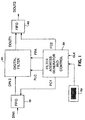
- a sampled data signal DIN1 is applied to a First In First Out (FIFO) memory circuit 10.
- Data samples are read from the FIFO 10 in response to control signal FC1 from filter address generator and control circuitry 30.
- FC1 control signal from filter address generator and control circuitry 30.
- CLK clock signal
- Digital filter 20 is a polyphase digital filter which uses samples provided by the FIFO 10 to generate new data samples of a resampled data signal DOUT1.
- a suitable interpolation filter for use in the filtering system is shown in U.S. Patent No. 5,331,346 entitled APPROXIMATING SAMPLE RATE CONVERSION SYSTEM issued to Shields et al.
- the digital filter in reality has many programmable filter characteristics and may be programmed as a time-division multiplexed (TDM) plurality of frequency characteristics. These TDM frequency characteristics are applied in a determined sequence to generate new data samples DOUT2 which can occur at a rate that may be different from the sampled data signal DIN1 when performing sample rate conversion.
- TDM time-division multiplexed
- the number of samples in a segment or a grid can be changed to produce a zoom in or zoom out effect.
- the input and output sample rates would be the same, however, the number of data sample values in a segment of data would be reduced or increased.
- a segment is, for example, a two dimensional portion of an image.
- the sample rate can be converted as well as the number of samples in a segment or grid.
- Such a system could be used in a wide screen television for displaying pictures in letter box format.
- the picture letter box format would be sample rate converted and the aspect ratio would be changed so that the picture conforms to the aspect ratio of the wide screen television.
- the digital filter 20 produces a new output data sample using the input data samples provided by FIFO 10.
- the digital filter uses a selected frequency characteristic to filter the input data samples to produce the new output data samples.
- the frequency characteristic is selected in response to a filter phase address location signal FPA from the generator and control circuitry 30.
- the resampled data values DOUT1 are supplied to a second FIFO memory 40 which, in turn, supplies the new data samples DOUT2 in response to a control signal FC2 from the generator and control circuitry 30.
- the generator and control circuitry 30 determines which of the plurality of the frequency characteristics of the polyphase digital filter 20 is used at a given time as provided by the signal FPA.
- the generator and control circuitry 30 determines which frequency characteristic to select using equations (4) and (5) below.
- X(i+1) (X(i)+C) mod (NPHASES*2 nbits )
- Q X(i+1) >> nbits
- the variables in equations (4) and (5) are X, the interpolation phase location, nbits, the number of bits for the phase quantization of the system, NPHASES, the fixed number of filters in the digital filter 20, i, the time index, Q, the quantized phase location, and C, the resampling factor.
- the >> operation in equation (5) is a right bit shift operation. nbits is selected to produce a desired resolution in the quantized phase location X. As the value of nbits is increased, the resolution of the quantized phase increases. The value of nbits is, however, limited by the size and speed of the adders required to implement equation (4). As the value of nbits increases the size of the adders increases and as a result, the speed of the adders may decrease.
- Equations (4) and (5) replace conventional equations (2) and (3).
- the ratio of the input sample rate value A and the output sample rate value B of equation (2) is preserved in the resampling factor value C.
- the ratio of the input sample rate value A to the output sample rate value B is expressed in equation (6) below.
- the resampling factor C is determined by equation (7) below.
- C (A/B) * NPHASES * 2 nbits
- the resampling factor is calculated once for a particular input sample rate value A and an output sample rate value B.
- the resampling factor can be calculated by generator and control circuitry 30 prior to resampling or provided to generator and control circuitry via input circuitry 50.
- the quantized phase is calculated for different input samples according to equations (4) and (5) using addition and bit shift operations, thus avoiding the repetitive use of the computationally expensive division and multiplication operations of equations (2) and (3).
- A is the number of samples provided to the digital filter in a first predetermined segment and B is the number of samples produced by the digital filter in a second predetermined segment.
- the first and second segments are equal but the number of data values in the first and second predetermined segments are different to produce a zooming effect.
- the number of data samples SAMP_IN provided to the digital filter is determined by a multiplication coefficient value m and whether a carryout is generated in calculating the resampled data.
- the multiplication coefficient value is the integer portion of the input sample rate divided by the output sample rate.
- A is the number of samples in an input line or segment and B is the number of data samples in an output line or segment.
- the first step in the process illustrated by this flow-chart, step 410 obtains input variables from input circuitry 50, shown in Fig. 1, used by the control and address circuitry 30.
- the input variables are A, the input sample rate, B, the output sample rate, NBITS, the number of bits for the phase quantization of the system, and NPHASES, the maximum number of filters in the digital filter 20.
- the process next determines whether the input sample rate A is greater than the output sample rate B. If the value of A is greater than the value of B, then down sampling is performed. If the value of A is less than the value of B, then upsampling is performed.
- a multiplication co-efficient m is calculated at step 432.
- the multiplication coefficient value is calculated so that it can be determined how many data samples must be provided to the digital filter to produce valid resampled data. For example, if the multiplication coefficient m is two, at least two samples values are provided to the filter 20 to produce a resampled output value.
- the multiplication coefficient value m is determined according to equation (8) below.
- M Int (A/B) Int takes the integer portion of A divided by B.
- the input sample rate value A is set to be equal to the input sample rate value A minus the multiplication coefficient value m multiplied by the output sample rate value B as shown in equation (9).
- A A - m * B
- the new calculated value A is then used, at step 428, to calculate the re-sampling factor value C shown in equation (10) below.
- C (A/B) * NPHASES *2 nbits
- the multiplication factor m is also used to determine the number of sample data to be provided to the digital filter 20 at any sampling instant to generate a new data sample at step 440.
- the generator and control circuitry 30 would control FIFO 10 using control signal FC1 to provide m sample data values DIN2 to the digital filter for each output sample DOUT1 produced by the filter in accordance with the value of SAMP_IN.
- the generator and control circuitry 30 would also provide a control signal FC2 to FIFO 40 to control which of the new data samples DOUT1 are accepted by FIFO 40.
- FC2 control signal
- the digital filter 20 produces a valid new data sample for every two data samples supplied to it. An invalid new data sample will be produced every other valid input sample, however, because the filter 20 produces a resampled data value DOUT1 for each data sample DIN2 provided to it. The invalid data samples produced between the new valid data samples are discarded.
- the address generator and control 30 provides a control signal FC2 to FIFO 40 to discard a new data sample DOUT1 when it is invalid.
- the new data samples DOUT1 are discarded until the correct number of data samples have been provided to digital filter 20 to produce a valid new data sample DOUT1. In this case, two samples are provided to digital filter 20 to produce each valid new data sample.
- a quantized phase location which is provided to the digital filter 20 as an address to select a particular frequency characteristic, is valid even though the corresponding new data sample is invalid and will be discarded. Accordingly, the quantized phase location is retained and used again after an additional sampled data value is provided to digital filter 20.
- digital filter 20 could be replaced with another digital filter which does not produce a new data sample until the correct number of data samples have been provided to the digital filter.
- the multiplication factor m is set equal to 0. Accordingly, the original input sample rate A is subsequently used at step 428 to calculate the resample factor C.
- the resampling factor is used to calculate the quantized phase.
- Fig. 3 shows an embodiment of the filter address generator and control circuitry 30 shown in Fig. 1.
- the interpolation phase location for a current sample is determined.
- An interpolation phase location value X(i) is provided to comparator 1410 to determine if the value of X(i) is greater than or equal to a comparator value COMP_VAL determined by equation (14) below.
- COMP_VAL NPHASES * 2 nbits - C
- the value of X(i) is not greater than the value of COMP_VAL, then the value of SUM_1 produced by adder 1420 is selected by multiplexer 1430 in response to a select signal SEL from comparator 1410. The value of X(i) is added to the re-sample factor value C at adder 1420.
- multiplexer 1430 selects the value of SUM_2 provided by adder 1425 in response to a select signal SEL from comparator 1410.
- the new interpolation phase location value X(i+1) provided by multiplexer 1430 is supplied as an input to comparator 1410 and as an input to the shifter 1440.
- Comparator 1410 uses the new interpolation phase location value X(i+1) as the current interpolation phase location value X(i) to calculate the next value of X(i+1).
- the filter phase address location signal FPA is retained in the address memory and counter 1450 and provided again to digital filter 20 in response to signal CO to calculate the next resampled data value DOUT1 after the next data sample DIN2 is provided to digital filter 20 as shown in Fig. 1.
- the address and counter circuitry maintains a count so that the new data samples provided by digital filter 20 can be provided to FIFO 40, shown in Fig. 1, or discarded in response to signal FC2 provided by address memory counter 1450.
- the digital filter after producing a resampled data value does not immediately provide the new data sample to FIFO 40. Accordingly, the count is maintained so that as the new data samples are provided to FIFO 40, control signal FC2 can be used to direct which new data samples FIFO 40 accepts.
- the generator and control circuitry When a carryout has been generated, the generator and control circuitry provides a control signal FC1 to FIFO 10 to shift in the next data sample. Then, the generator and control circuitry 30 repeats the previous filter phase address location signal FPA which has been stored in the address memory and control circuitry 1450 to produce the new data sample.
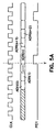
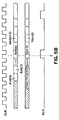
- the filter phase address location "ADR(n)" is used by the digital filter 20 to select a frequency characteristic to produce a new data sample. If a carryout has been generated, as shown at time T, then, the next sampled data value is provided to digital filter 20 and filter phase address location ADR(n) is reused by the digital filter 20 to produce the new data sample using the next data sample. In addition, a control signal FC2 is subsequently provided to FIFO 40 to discard the new data sample which was calculated when the carryout was generated.
- FIFO 40 When upsampling, FIFO 40 accepts new data samples whether the value of X(i) is less than, greater than, or equal to the value of COMP_VAL. FIFO 10, however, does not shift in the next sampled data if the value of X(i) is not greater than the value of COMP_VAL. Digital filter 30 calculates the next new data sample using the data samples it already contains. The next data sample value DIN2 is provided to digital filter 30 from FIFO 10 if the interpolation phase location value X(i) is greater than or equal to the value of COMP_VAL.
- the shift register 1440 shifts the value of X(i+1) right by the value of nbits (i.e. divides X(i+1) by 2 nbits ) to produce a quantized phase value Q.
- the value of Q is provided to digital filter 20 as the filter phase address location signal FPA which uses the filter phase address location signal FPA to select a frequency characteristic of the digital filter 20 to filter the current data samples.
- the generator and control circuitry 30 uses equations (16), (17) and (18) below to calculate the quantized phase value.
- X(i+1) (X(i)+ZI+COY) mod NPHASES
- Y(i+1) (Y(i) + ZF) mod m
- COY (Y(i) + ZF) ⁇ m
- the variables in equations (16) (17), and (18), are X, the interpolation phase location, NPHASES, the fixed number of filters in the digital filter 20, i, the time index, Y, the adder value, m, the size of the adder calculating the value of Y(i) added to ZF, and COY, a carryout produced by the adder calculating the value of Y(i) added to ZF.
- the ⁇ in equation (18) is a logical operation which is only used to express an overflow, a carryout, produced by the adder which adds Y(i) to ZF. If a carryout COY is produced, it is used in equation (16) to calculate the interpolation phase location.
- ZI is the s-r most significant bits of the resampling factor C and ZF is the r least significant bits of the resampling factor C as shown in equations (19) and (20) where the resampling factor C has s bits and r is equal to the value of nbits.
- ZI C[s:r]
- ZF C[(r-1):0]
- the resampling factor is determined using equation (7).
- the resampling factor is calculated once for a particular input sample rate value A and a output sample rate value B.
- the quantized phase repetitively calculated for different input samples is determined according to equations (16) and (17) using addition and bit shift operations, thus avoiding the use of the computationally expensive division and multiplication operations.
- Xint(i+1) Xint(i+1) - NPHASES
- the quantized phase value Q is set equal to the value of Xint(i+1).
- the filter phase address location signal FPA corresponding to the quantized phase value Q is provided to digital filter 20 to choose the frequency characteristic.
- the value of Xint(i+1) is used as the value of Xint(i) to repeat the process.
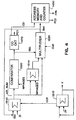
- Fig. 4 shows the filter address generator and control circuitry 30 shown in Fig. 1.
- a first adder 1510 is supplied with the s-r most significant bits of the resampling factor data C as the value ZI where s-r is determined according to equation (19) and (20). The value of ZI is added to the value of Xint(i) to produce the value of XZI_SUM.
- adder 1512 is supplied with the r least significant bits of the resampling factor data C as the value ZF.
- the adder 1512 adds the value of ZF with the value of Y(i). If this addition produces a carryout value COY, the value of COY is provided to adder 1510 to be added to the values of ZI and Xint(i) to produce the value of XZI_SUM.
- the value of Y is also provided as an input to adder 1512.
- the adder 1512 is started prior to adder 1510. As a result, if adder 1512 generates a carryout COY, the carryout COY can be provided to adder 1510 to be added to the corresponding values of Xint(i) and ZI.
- the initial values of Y and X are selected according to the particular application of the resampling circuit.
- the value of XZI_SUM is compared to the value of NPHASES at comparator 1520. If the value of XZI_SUM is less than the value of NPHASES, multiplexer 1530 selects the value XZI_SUM and provides it as an output Xint(i+1) in response to a select signal SEL from comparator 1520. If the value of XZI_SUM is greater than or equal to the value of NPHASES, multiplexer 1530 selects the value of MPHASES subtracted from XZI_SUM at adder 1514 and provides it as an output Xint(i+1) in response to the select signal SEL supplied by multiplexer 1530.
- the output value Xint(i+1) provided by multiplexer 1530 is provided to the digital filter 20 via the filter phase address location signal FPA to identify a frequency characteristic in the digital filter 20 which is to be used to filter the data samples.
- the output value Xint(i+1) provided by multiplexer 1530 is also provided as an input value to adder 1510.
- the address memory and counter 1450 and carryout toggle circuitry 1470 perform the same functions as the corresponding reference numerals in Fig. 3.
Landscapes
- Engineering & Computer Science (AREA)
- Physics & Mathematics (AREA)
- Computer Hardware Design (AREA)
- Mathematical Physics (AREA)
- Computing Systems (AREA)
- Theoretical Computer Science (AREA)
- Computer Graphics (AREA)
- Multimedia (AREA)
- Signal Processing (AREA)
- Transmission Systems Not Characterized By The Medium Used For Transmission (AREA)
- Compression Or Coding Systems Of Tv Signals (AREA)
- Television Systems (AREA)
Claims (16)
- Digitales Wiederabtastsystem mit
einem Interpolations-Filter (20) mit einer Mehrzahl von Phasen, wobei jede Phase eine jeweils andere interpolierte Abtastposition darstellt; und
einer Filter-Auswahlvorrichtung (30) zum Erzeugen einer Sequenz von Filter-Adress-Werten (Q) für den Interpolationsfilter, wobei die Sequenz der Filter-Adress-Werte eine jeweilige Sequenz von Phasen des Interpolations-Filters bezeichnet, welche verwendet wird, um erste Daten von einem ersten Segment von Daten wiederabzutasten, um zweite abgetastete Daten in einem zweiten Segment von Daten zu erzeugen,
dadurch gekennzeichnet, dass die Filter-Auswahlvorrichtung aufweist:eine Vorrichtung (1420) zum Addieren eines Wiederabtast-Faktors (C) zu einem vorherigen Adress-Wert (X(i)), um einen ersten aktuellen Adress-Wert (SUM_1) zu erzeugen;eine Vorrichtung (1425) zum Subtrahieren eines Komparator-Wertes (NPHASES*2nbits-C) von dem vorherigem Adress-Wert (X(i)) um einen zweiten aktuellen Adress-Wert (SUM_2) zu erzeugen;eine Vorrichtung (1430) zum Auswählen des ersten aktuellen Adress-Wertes (SUM_1) als den aktuellen Adress-Wert (X(i+1)) wenn der vorherige Adress-Wert (X(i)) weniger ist als der Komparator-Wert (NPHASES*2nbits-C) und zum Auswählen des zweiten aktuellen Adress-Wertes (SUM_2) als den aktuellen Adress-Wert (X(i+1)), wenn dervorherige Adress-Wert (X(i)) nicht weniger ist als der Komparator-Wert (NPHASES*2nbits-C); undeine Vorrichtung (1440) zum Verschieben des aktuellen Adress-Wertes (X(i+1)) um nbits Bits, um den Filter-Adress-Wert (Q) zu erzeugen, wobei nbits eine ganze Zahl ist und eine Anzahl von Bits einer Phasen-Quantisierung für den Interpolations-Filter definiert. - Digitales Wiederabtastsystem nach Anspruch 1, wobei die Anzahl der Phasen des Interpolations-Filters (20) gleich NPHASES ist, und der Komparator-Wert ist gleich NPHASES*2nbits-C, wobei C der Wiederabtast-Faktor ist.
- Digitales Wiederabtastsystem nach Anspruch 1, wobei die Anzahl der Phasen des Interpolations-Filters (20) gleich NPHASES ist, und der Wiederabtast-Faktor-Wert (C) ist gleich (A/B)* NPHASES*2nbits, wobei A ein Wert ist, welcher eine Menge der ersten Daten in dem ersten Segment der Daten darstellt, und B ist ein Wert, welcher eine Menge der zweiten Daten in dem zweiten Segment von Daten darstellt.
- Digitales Wiederabtastsystem nach Anspruch 1, wobei das System geeignet ist, um das wiederabgetastete zweite Segment von Daten so zu erzeugen, dass das zweite Segment von Daten gleich dem ersten Segment von Daten ist und die Menge der zweiten Daten ist von der Menge der ersten Daten verschieden, zum Erzeugen eines Zoom-Effekts.
- Digitales Wiederabtastsystem nach Anspruch 1, wobei das System geeignet ist, um das wiederabgetastete zweite Segment von Daten so zu erzeugen, dass das zweite Segment der Daten von dem ersten Segment der Daten verschieden ist, zum Durchführen einer Abtast-Raten-Umwandlung.
- Digitales Wiederabtastsystem mit
einem Interpolations-Filter (20) mit Mehrzahl von Phasen, wobei jede Phase eine jeweils andere interpolierte Abtastposition darstellt; und .
einer Filter-Auswahlvorrichtung (30) zum Erzeugen einer Sequenz von Filter-Adress-Werten (Q) für den Interpolationsfilter, wobei die Sequenz der Filter-Adress-Werte eine jeweilige Sequenz von Phasen des Interpolations-Filters bezeichnet, welche verwendet wird, um erste Daten von einem ersten Segment von Daten wiederabzutasten, um zweite abgetastete Daten in einem zweiten Segment von Daten zu erzeugen,
dadurch gekennzeichnet, dass der Filter-Selektor aufweist:eine Vorrichtung zum Empfangen eines Wiederabtast-Faktor-Wertes (C) mit s-bits: s-r höchstwertigen Bits (MSBs) und r niederwertigsten Bits (LSBs), wobei s und r ganze Zahlen sind;einen ersten Addierer (1512) zum Addieren eines früheren bzw. vorangehenden Addier-Wertes (Y(i)) zu den r LSBs (ZF) des Wiederabtast-Faktors (C), um ein Stellenübertrags-Wert (COY) zu erzeugen;einen zweiten Addierer (1510) zum Addieren eines vorherigen Filter-Adress-Wertes Xint(i) und der s-r MSBs (ZI) des Wiederabtast-Faktors (C) und des Stellenübertrags-Wertes (COY), um einen ersten Adress-Wert (XZI_SUM) zu erzeugen;eine Vorrichtung (1514) zum Subtrahieren eines Komparator-Wertes (NPHASES) von dem ersten Adress-Wert (XZI_SUM) um einen zweiten Adress-Wert zu erzeugen;eine Vorrichtung (1520, 1530) zum Auswählen des ersten Adress-Wertes (XZI_SUM) als den quantisierten Adress-Wert (Q), wenn der erste Adress-Wert (XZI_SUM) kleiner ist als der Komparator-Wert (NPHASES) und zum Auswählen des zweiten Adress-Wertes als den quantisierten Adress-Wert (Q), wenn der erste Adress-Wert (XZI_SUM) nicht kleiner ist als der Komparator-Wert (NPHASES). - Digitales Wiederabtastsystem nach Anspruch 6, wobei der Komparator-Wert (NPHASES) gleich der Anzahl der Phasen des Interpolationsfilters ist.
- Digitales Wiederabtastsystem nach Anspruch 6, wobei die Anzahl der Phasen des Interpolations-Filters (20) gleich NPHASES ist, und der Wiederabtast-Faktor-Wert (C) ist gleich (A/B) * NPHASES*2nbits, wobei A ein Wert ist, welcher eine Menge der ersten Daten in dem ersten Segment von Daten darstellt, und B ist ein Wert, welcher eine Menge der zweiten Daten in dem zweiten Segment von Daten darstellt, und nbits ist eine ganze Zahl, welche eine Anzahl von Bits der Phasen-Quantisierung für den Interpolations-Filter definiert.
- Digitales Wiederabtastsystem nach Anspruch 8, wobei der Wert von r gleich dem Wert von nbits ist.
- Digitales Wiederabtastsystem nach Anspruch 6, wobei der Wert von r eine Auflösung des Filter-Adress-Wertes definiert.
- Verfahren zum Erzeugen einer Filter-Adresse für einen Interpolations-Filter in einem digitalen Wiederabtastsystem, wobei der Interpolations-Filter eine Mehrzahl von adressierbaren Phasen aufweist, wobei das Verfahren die Schritte aufweist:Addieren eines vorherigen Adress-Wertes (X(i)) und eines Wiederabtast-Faktors (C), um einen ersten aktuellen Adress-Wert (SUM_1) zu erzeugen;Subtrahieren eines Komparator-Wertes (NPHASES*2nbits-C) von dem vorherigen Adress-Wert (X(i)), um einen zweiten aktuellen Adress-Wert (SUM_2) zu erzeugen;Auswählen des ersten aktuellen Adress-Wertes (SUM_1) als den aktuellen Adress-Wert (X(i+1)), wenn der vorherige Adress-Wert (X(i)) kleiner ist als der Komparator-Wert (NPHASES*2nbits-C);Auswählen des zweiten Adress-Wertes (SUM_2) als den aktuellen Adress-Wert (X(i+1)), wenn der vorherige Adress-Wert (X(i)) nicht kleiner ist als der Komparator-Wert (NPHASES*2nbits-C);Verschieben der aktuellen Filter-Adresse (X(i+1)) um nbits Bits, um den Filter-Adress-Wert (Q) zu erzeugen, wobei nbits eine ganze Zahl ist, welche eine Anzahl von Bits einer Phasen-Quantisierung für den Interpolations-Filter definiert.
- Verfahren nach Anspruch 11, wobei die Anzahl der Phasen des Interpolations-Filters (20) gleich NPHASES ist, und der Komparator-Wert ist gleich NPHASES*2nbits-C, wobei C der Wiederabtast-Faktor ist.
- Verfahren nach Anspruch 11, wobei die Anzahl der Phasen des Interpolations-Filters (20) gleich NPHASES ist, und der Wiederabtast-Faktor-Wert (C) ist gleich (A/B)* NPHASES*2nbits, wobei A ein Wert ist, welcher eine Menge der ersten Daten in dem ersten Segment der Daten darstellt, und B ist ein Wert, welcher eine Menge der zweiten Daten in dem zweiten Segment von Daten darstellt.
- Verfahren zum Erzeugen einer Filter-Adresse für einen Interpolations-Filter in einem digitalen Wiederabtastsystem, wobei der Interpolations-Filter. eine Mehrzahl von adressierbaren Phasen hat und das Verfahren weist die Schritte auf:Empfangen eines Wiederabtast-Faktor-Werts (C) mit s-Bits: s-r höchstwertigen Bits (MSBs) und r niederwertistgen Bits (LSBs), wobei r und s ganze Zahlen sind;Addieren eines vorherigen Addier-Wertes (Y(i)) zu den r LBSs (ZF) des Wiederabtast-Faktors (C), um einen Stellenübertrags-Wert (COY) zu erzeugen;Addieren eines vorherigen Filter-Adress-Wertes Xint(i) und der s-r MSBs (ZI) des Wiederabtast-Faktors (C) und des Stellenübertrags-Wertes (COY), um einen ersten Adress-Wert (XZI_SUM) zu erzeugen;Subtrahieren eines Komparator-Wertes (NPHASES) von dem ersten Adress-Wert (XZI_SUM), um einen zweiten Adress-Wert zu erzeugen;Auswählen des ersten Adress-Wertes (XZI_SUM) als den quantisierten Adress-Wert (Q), wenn der erste Adress-Wert (XZI_SUM) kleiner ist als der Komparator-Wert (NPHASES) und Auswählen des zweiten Adress-Wertes als den quantisierten Adress-Wert (Q), wenn der erste Adress-Wert (XZI_SUM) nicht kleiner ist als der Komparator-Wert (NPHASES).
- Verfahren nach Anspruch 14, wobei der Komparator-Wert (NPHASES) gleich der Anzahl der Phasen des Interpolations-Filters ist.
- Verfahren nach Anspruch 14, wobei die Anzahl der Phasen des Interpolations-Filters (20) gleich NPHASES ist, und der Wiederabtast-Faktor-Wert (C) ist gleich (A/B) * NPHASES *2nbits, wobei A ein Wert ist, welcher eine Menge der ersten Daten in dem ersten Segment von Daten darstellt, und B ist ein Wert, welcher eine Menge der zweiten Daten in dem zweiten Segment von Daten darstellt, und nbits ist eine ganze Zahl, welche eine Anzahl von Bits der Phasen-Quantisierung für den Interpolations-Filter definiert.
Applications Claiming Priority (2)
| Application Number | Priority Date | Filing Date | Title |
|---|---|---|---|
| US317474 | 1994-10-04 | ||
| US08/317,474 US5613084A (en) | 1994-10-04 | 1994-10-04 | Interpolation filter selection circuit for sample rate conversion using phase quantization |
Publications (3)
| Publication Number | Publication Date |
|---|---|
| EP0706262A2 EP0706262A2 (de) | 1996-04-10 |
| EP0706262A3 EP0706262A3 (de) | 1997-11-19 |
| EP0706262B1 true EP0706262B1 (de) | 2002-07-24 |
Family
ID=23233818
Family Applications (1)
| Application Number | Title | Priority Date | Filing Date |
|---|---|---|---|
| EP95115356A Expired - Lifetime EP0706262B1 (de) | 1994-10-04 | 1995-09-28 | Filterauswahlschaltung für ein digitales Wiederabtastsystem |
Country Status (4)
| Country | Link |
|---|---|
| US (1) | US5613084A (de) |
| EP (1) | EP0706262B1 (de) |
| JP (1) | JPH08181950A (de) |
| DE (1) | DE69527482T2 (de) |
Families Citing this family (13)
| Publication number | Priority date | Publication date | Assignee | Title |
|---|---|---|---|---|
| US5617088A (en) * | 1994-01-26 | 1997-04-01 | Sony Corporation | Sampling frequency converting device and memory address control device |
| TW348266B (en) * | 1996-03-11 | 1998-12-21 | Toshiba Co Ltd | Semiconductor memory device |
| US6175592B1 (en) | 1997-03-12 | 2001-01-16 | Matsushita Electric Industrial Co., Ltd. | Frequency domain filtering for down conversion of a DCT encoded picture |
| US6618443B1 (en) | 1997-03-12 | 2003-09-09 | Matsushita Electric Industrial Co., Ltd. | Upsampling filter for a down conversion system |
| WO1998041012A1 (en) | 1997-03-12 | 1998-09-17 | Matsushita Electric Industrial Co., Ltd. | Mpeg decoder providing multiple standard output signals |
| US6788347B1 (en) * | 1997-03-12 | 2004-09-07 | Matsushita Electric Industrial Co., Ltd. | HDTV downconversion system |
| US7554612B2 (en) * | 2000-10-03 | 2009-06-30 | Thomson Licensing | Method and system for buffering pixel data |
| US7053896B2 (en) * | 2001-02-07 | 2006-05-30 | Micron Technology, Inc. | Resampling system and method for graphics data including sine-wave components |
| US6531969B2 (en) * | 2001-05-02 | 2003-03-11 | Portalplayer, Inc. | Resampling system and apparatus |
| EP1741282A1 (de) * | 2004-04-30 | 2007-01-10 | Nvidia Corporation | Verfahren und vorrichtung zur vertikalen skalierung von pixeldaten |
| US8904299B1 (en) * | 2006-07-17 | 2014-12-02 | The Mathworks, Inc. | Graphical user interface for analysis of a sequence of data in object-oriented environment |
| US7583771B2 (en) * | 2006-08-22 | 2009-09-01 | Schweitzer Engineering Laboratories, Inc. | Systems and methods for resampling unreliable data |
| US9030337B2 (en) * | 2013-10-07 | 2015-05-12 | Telefonaktiebolaget L M Ericsson (Publ) | Multi-branch down converting fractional rate change filter |
Family Cites Families (9)
| Publication number | Priority date | Publication date | Assignee | Title |
|---|---|---|---|---|
| JPS58219841A (ja) * | 1982-06-15 | 1983-12-21 | Kokusai Denshin Denwa Co Ltd <Kdd> | 標本化周波数の高速変換回路 |
| JP2592810B2 (ja) * | 1986-09-30 | 1997-03-19 | 株式会社東芝 | サンプルレート変換回路 |
| US4774581A (en) * | 1987-04-14 | 1988-09-27 | Rca Licensing Corporation | Television picture zoom system |
| EP0356597B1 (de) * | 1988-08-30 | 1994-03-30 | International Business Machines Corporation | Massnahmen zur Verbesserung des Verfahrens und Vorrichtung eines digitalen Frequenzumsetzungsfilters |
| US5057911A (en) * | 1989-10-19 | 1991-10-15 | Matsushita Electric Industrial Co., Ltd. | System and method for conversion of digital video signals |
| JP3255179B2 (ja) * | 1992-02-14 | 2002-02-12 | ソニー株式会社 | データ検出装置 |
| US5475628A (en) * | 1992-09-30 | 1995-12-12 | Analog Devices, Inc. | Asynchronous digital sample rate converter |
| US5331346A (en) * | 1992-10-07 | 1994-07-19 | Panasonic Technologies, Inc. | Approximating sample rate conversion system |
| US5274372A (en) * | 1992-10-23 | 1993-12-28 | Tektronix, Inc. | Sampling rate conversion using polyphase filters with interpolation |
-
1994
- 1994-10-04 US US08/317,474 patent/US5613084A/en not_active Expired - Lifetime
-
1995
- 1995-09-28 EP EP95115356A patent/EP0706262B1/de not_active Expired - Lifetime
- 1995-09-28 DE DE69527482T patent/DE69527482T2/de not_active Expired - Fee Related
- 1995-10-04 JP JP7257718A patent/JPH08181950A/ja not_active Withdrawn
Also Published As
| Publication number | Publication date |
|---|---|
| US5613084A (en) | 1997-03-18 |
| EP0706262A2 (de) | 1996-04-10 |
| DE69527482T2 (de) | 2003-05-08 |
| DE69527482D1 (de) | 2002-08-29 |
| EP0706262A3 (de) | 1997-11-19 |
| JPH08181950A (ja) | 1996-07-12 |
Similar Documents
| Publication | Publication Date | Title |
|---|---|---|
| EP0706262B1 (de) | Filterauswahlschaltung für ein digitales Wiederabtastsystem | |
| EP1331817B1 (de) | Vorrichtung zur Umsetzung von digitalen Daten | |
| JP3297165B2 (ja) | 標本化周波数変換器 | |
| US5374995A (en) | Method and apparatus for enhancing sharpness of a sequence of images subject to continuous zoom | |
| US5621404A (en) | Digital-to-digital sample rate converter | |
| EP0800687B1 (de) | Digitales videoumwandlungsschaltsystem | |
| JP2646532B2 (ja) | 信号補間回路 | |
| EP0690621B1 (de) | Abtastratenumsetzer und Verfahren zur Abtastratenumsetzung | |
| KR100475201B1 (ko) | 샘플레이트를변경하는필터디바이스및영상디스플레이장치 | |
| EP0629044B1 (de) | Digitale Signalverarbeitung | |
| WO1993014592A1 (en) | Digital image interpolation system for zoom and pan effects | |
| US5410616A (en) | Loop-up table image scaling for rational factors | |
| US5159339A (en) | Sampling rate converter for signals having a non-integer sampling ratio | |
| JP3287934B2 (ja) | デジタルフィルタ及びそのろ波方法 | |
| EP1304650B1 (de) | Einrichtung und Verfahren zur Bildskalierung | |
| JP2008054344A (ja) | 非同期データをディジタル信号に挿入する方法及び装置 | |
| US6288794B1 (en) | Variable sample rate converter adaptable to rational ratios | |
| GB2236452A (en) | Determining interpolation weighting coefficients for low ratio sampling rate converter | |
| US7990472B2 (en) | Generalized VBI waveform generator | |
| KR970009447B1 (ko) | 텔레비젼수상기의 영상신호 수직변환 회로 | |
| JP3151288B2 (ja) | 画像要素変換処理装置 | |
| JP3352116B2 (ja) | 画像処理装置 | |
| JP3257145B2 (ja) | 撮像装置 | |
| JPH05191722A (ja) | 画像拡大装置 | |
| WO1993005617A1 (en) | Sample rate convertor |
Legal Events
| Date | Code | Title | Description |
|---|---|---|---|
| PUAI | Public reference made under article 153(3) epc to a published international application that has entered the european phase |
Free format text: ORIGINAL CODE: 0009012 |
|
| AK | Designated contracting states |
Kind code of ref document: A2 Designated state(s): DE FR NL |
|
| PUAL | Search report despatched |
Free format text: ORIGINAL CODE: 0009013 |
|
| AK | Designated contracting states |
Kind code of ref document: A3 Designated state(s): DE FR NL |
|
| 17P | Request for examination filed |
Effective date: 19980519 |
|
| 17Q | First examination report despatched |
Effective date: 20000918 |
|
| GRAG | Despatch of communication of intention to grant |
Free format text: ORIGINAL CODE: EPIDOS AGRA |
|
| GRAG | Despatch of communication of intention to grant |
Free format text: ORIGINAL CODE: EPIDOS AGRA |
|
| GRAH | Despatch of communication of intention to grant a patent |
Free format text: ORIGINAL CODE: EPIDOS IGRA |
|
| GRAH | Despatch of communication of intention to grant a patent |
Free format text: ORIGINAL CODE: EPIDOS IGRA |
|
| GRAH | Despatch of communication of intention to grant a patent |
Free format text: ORIGINAL CODE: EPIDOS IGRA |
|
| GRAA | (expected) grant |
Free format text: ORIGINAL CODE: 0009210 |
|
| AK | Designated contracting states |
Kind code of ref document: B1 Designated state(s): DE FR NL |
|
| REF | Corresponds to: |
Ref document number: 69527482 Country of ref document: DE Date of ref document: 20020829 |
|
| ET | Fr: translation filed | ||
| PLBE | No opposition filed within time limit |
Free format text: ORIGINAL CODE: 0009261 |
|
| STAA | Information on the status of an ep patent application or granted ep patent |
Free format text: STATUS: NO OPPOSITION FILED WITHIN TIME LIMIT |
|
| 26N | No opposition filed |
Effective date: 20030425 |
|
| PGFP | Annual fee paid to national office [announced via postgrant information from national office to epo] |
Ref country code: NL Payment date: 20040905 Year of fee payment: 10 |
|
| PGFP | Annual fee paid to national office [announced via postgrant information from national office to epo] |
Ref country code: FR Payment date: 20040908 Year of fee payment: 10 |
|
| PGFP | Annual fee paid to national office [announced via postgrant information from national office to epo] |
Ref country code: DE Payment date: 20040923 Year of fee payment: 10 |
|
| PG25 | Lapsed in a contracting state [announced via postgrant information from national office to epo] |
Ref country code: NL Free format text: LAPSE BECAUSE OF NON-PAYMENT OF DUE FEES Effective date: 20060401 Ref country code: DE Free format text: LAPSE BECAUSE OF NON-PAYMENT OF DUE FEES Effective date: 20060401 |
|
| PG25 | Lapsed in a contracting state [announced via postgrant information from national office to epo] |
Ref country code: FR Free format text: LAPSE BECAUSE OF NON-PAYMENT OF DUE FEES Effective date: 20060531 |
|
| NLV4 | Nl: lapsed or anulled due to non-payment of the annual fee |
Effective date: 20060401 |
|
| REG | Reference to a national code |
Ref country code: FR Ref legal event code: ST Effective date: 20060531 |