EP0706186A2 - DRAM-Speicheranordnungen - Google Patents
DRAM-Speicheranordnungen Download PDFInfo
- Publication number
- EP0706186A2 EP0706186A2 EP95307110A EP95307110A EP0706186A2 EP 0706186 A2 EP0706186 A2 EP 0706186A2 EP 95307110 A EP95307110 A EP 95307110A EP 95307110 A EP95307110 A EP 95307110A EP 0706186 A2 EP0706186 A2 EP 0706186A2
- Authority
- EP
- European Patent Office
- Prior art keywords
- pins
- dram
- data
- addressing
- write
- Prior art date
- Legal status (The legal status is an assumption and is not a legal conclusion. Google has not performed a legal analysis and makes no representation as to the accuracy of the status listed.)
- Withdrawn
Links
Images




Classifications
-
- G—PHYSICS
- G11—INFORMATION STORAGE
- G11C—STATIC STORES
- G11C11/00—Digital stores characterised by the use of particular electric or magnetic storage elements; Storage elements therefor
- G11C11/21—Digital stores characterised by the use of particular electric or magnetic storage elements; Storage elements therefor using electric elements
- G11C11/34—Digital stores characterised by the use of particular electric or magnetic storage elements; Storage elements therefor using electric elements using semiconductor devices
- G11C11/40—Digital stores characterised by the use of particular electric or magnetic storage elements; Storage elements therefor using electric elements using semiconductor devices using transistors
- G11C11/401—Digital stores characterised by the use of particular electric or magnetic storage elements; Storage elements therefor using electric elements using semiconductor devices using transistors forming cells needing refreshing or charge regeneration, i.e. dynamic cells
- G11C11/4063—Auxiliary circuits, e.g. for addressing, decoding, driving, writing, sensing or timing
- G11C11/407—Auxiliary circuits, e.g. for addressing, decoding, driving, writing, sensing or timing for memory cells of the field-effect type
- G11C11/408—Address circuits
-
- G—PHYSICS
- G11—INFORMATION STORAGE
- G11C—STATIC STORES
- G11C5/00—Details of stores covered by group G11C11/00
- G11C5/06—Arrangements for interconnecting storage elements electrically, e.g. by wiring
- G11C5/066—Means for reducing external access-lines for a semiconductor memory clip, e.g. by multiplexing at least address and data signals
-
- G—PHYSICS
- G11—INFORMATION STORAGE
- G11C—STATIC STORES
- G11C11/00—Digital stores characterised by the use of particular electric or magnetic storage elements; Storage elements therefor
- G11C11/21—Digital stores characterised by the use of particular electric or magnetic storage elements; Storage elements therefor using electric elements
- G11C11/34—Digital stores characterised by the use of particular electric or magnetic storage elements; Storage elements therefor using electric elements using semiconductor devices
- G11C11/40—Digital stores characterised by the use of particular electric or magnetic storage elements; Storage elements therefor using electric elements using semiconductor devices using transistors
- G11C11/401—Digital stores characterised by the use of particular electric or magnetic storage elements; Storage elements therefor using electric elements using semiconductor devices using transistors forming cells needing refreshing or charge regeneration, i.e. dynamic cells
- G11C11/4063—Auxiliary circuits, e.g. for addressing, decoding, driving, writing, sensing or timing
- G11C11/407—Auxiliary circuits, e.g. for addressing, decoding, driving, writing, sensing or timing for memory cells of the field-effect type
- G11C11/409—Read-write [R-W] circuits
- G11C11/4093—Input/output [I/O] data interface arrangements, e.g. data buffers
-
- G—PHYSICS
- G11—INFORMATION STORAGE
- G11C—STATIC STORES
- G11C11/00—Digital stores characterised by the use of particular electric or magnetic storage elements; Storage elements therefor
- G11C11/21—Digital stores characterised by the use of particular electric or magnetic storage elements; Storage elements therefor using electric elements
- G11C11/34—Digital stores characterised by the use of particular electric or magnetic storage elements; Storage elements therefor using electric elements using semiconductor devices
- G11C11/40—Digital stores characterised by the use of particular electric or magnetic storage elements; Storage elements therefor using electric elements using semiconductor devices using transistors
- G11C11/401—Digital stores characterised by the use of particular electric or magnetic storage elements; Storage elements therefor using electric elements using semiconductor devices using transistors forming cells needing refreshing or charge regeneration, i.e. dynamic cells
- G11C11/4063—Auxiliary circuits, e.g. for addressing, decoding, driving, writing, sensing or timing
- G11C11/407—Auxiliary circuits, e.g. for addressing, decoding, driving, writing, sensing or timing for memory cells of the field-effect type
- G11C11/409—Read-write [R-W] circuits
- G11C11/4096—Input/output [I/O] data management or control circuits, e.g. reading or writing circuits, I/O drivers or bit-line switches
Definitions
- the present invention relates to dynamic random access memory (DRAM) devices operating in either asynchronous or synchronous modes, being more particularly concerned with the increasing of the data bandwidth and addressing range of current DRAM devices, and/or providing equivalent bandwidth and addressing range thereof for smaller devices -- the invention attaining such results with a radically new and different interface and associated access mechanism than conventionally used with DRAM systems.
- DRAM dynamic random access memory
- SRAM static random access memory
- a Samsung Type KM644002 cmos SRAM was presented in a 32-pin plastic unit (400 mil) providing 1,048,576 words by 4 bits and using four common input and output lines and an output enable pin operating faster than the address access time at read cycle -- the fast access times ranging from 15 to 25 ns.
- 20 address bits are rejoined (20 of the pins being address pins) along with 4 data pins and control signals.
- DRAM dynamic random access memory
- the external circuit interface of the DRAM differs significantly from the SRAM. Contrasting the illustrative Samsung Type KM644002 SRAM above-described, with a corresponding Samsung Type KM44C1000B CMOS DRAM, as described on pages 330-337 of said Samsung catalog, the addressing is similar to uniquely identifying an element within a matrix, with each location in the address space being accessed by providing a row address and a column address. For the 1 million x 4 bit example, only a total of 20 address bits are required, 10 bits used to select the row in which the bit is located and 10 bits selecting the column of the desired bit in the selected row.
- the DRAM access mechanism is as follows. A 10 bit row address followed by a 10 bit column address are provided on the same pins sequentially by the external circuit, with the internal circuit using this sequentially provided information to select the desired unique location as described in the said catalog.
- the external circuit interface of this DRAM is asynchronous in nature and thus it is also called an asynchronous or async DRAM.
- This sequential occurrence of row and column addresses instead of presenting the entire address at the same time, however, delays the storage and retrieval of information compared to the SRAM, and as more particularly shown on said pages 336 and 337, for example, as compared with the SRAM read and write access cycles described on pages 299 and 300.
- a clock is provided in the SDRAM and all accesses are synchronous to the clock. It is optimized for burst transfer accesses and has substantially higher burst access speeds. After initial set up time, data is stored or retrieved every clock cycle for the whole burst.
- a typical 4M x 4 SDRAM and its internal structure is the micron type MT48 described on pages 2-1 and 2-2 of the Micron Semiconductor data book of 1994. The access mechanism for read and write cycles of SDRAM devices is described, for example, on pages 4-525 and 4-526 of the Texas Instruments catalog entitled MOS Memory, 1993, with such SDRAM having different access mechanisms than async DRAM and requiring different external circuits to generate the control signals.
- Granularity is another problem or issue with the existing DRAMs. There is no easy way to get odd sizes (sizes which are not multiples of 4) such as 2M x 64 or 6M x 64, without using large numbers of components. As an example, if it is desired to get a 6M x 64 memory configuration, then thirty two 4M x 4 devices are required.
- Pin-to-pin compatibility with successive generation exists only for a very narrow range.
- the package size grows quickly along with the density of the DRAM; and this forces redesigns to keep up with ever-increasing system memory requirements, since higher density chips require bigger footprints.
- the startling discovery underlying the present invention synergistically breaks through all these disadvantages and limitations enabling, for the same configuration, a reduced number of components; and, for comparable density, providing smaller package sizes with lower power consumption, lesser manufacturing and assembly costs, better MTBF, finer granularity, and greatly expanded pin compatibility for a wide range of DRAMs.
- the invention indeed, provides increased capability in data bandwidth and addressing range over current DRAM devices (using the same pin count and size device) or equivalent bandwidth and addressing range with smaller DRAM devices packages, both async and SDRAM. This is accomplished with a total departure from the direction uniformly taken in this art over the past decades, employing, rather, a novel interface and associated access mechanisms and procedure.
- An object of the present invention accordingly, is to provide a new and improved method of and apparatus for improving the data bandwidth and addressing range of current and past dynamic random access memory devices; either increasing the data bandwidth and addressing range for current-size devices of this character and/or providing equivalent bandwidth and addressing range thereof in smaller devices, all in obviation of the disadvantages and limitations of the prior art as previously described.
- a futher object is to provide a novel interface and associated addressing mechanism for dynamic random access memory devices.
- the invention embraces a method of improving the data bandwidth and addressing range capabilities of a dynamic random access memory device of the type conventionally having row and column address, data input, data output, and enable pins, and operating with addressing, data write and read cycle control lines connected with corresponding of said pins, the method comprising, on each of write and read cycles, respectively initially addressing row address on a predetermined set of the pins; then addressing on each of the write and read cycles, column address along the row on the same predetermined set of pins; then, on each of said write and read cycles, and following their respective column addressing, applying and retrieving data on the same predetermined set of pins during the respective write and read cycles, thereby reducing the number of pins required for addressing, writing and reading, and thus increasing data bandwidth and addressing range capabilities of the device.
- FIG. 1 is a plan view of an illustrative or exemplary 24-pin asynchronous 4M x 4 baseline asynchronous DRAM and control lines and pins adapted for the practice of the invention
- the invention (coined 'PARAS') has a distinct external circuit interface and a unique access mechanism which differ radically from the before-described existing techniques used by either the async DRAM or SDRAM.
- the row address is provided on a set of pins, followed by column address, and then data is transferred over the same pins.
- the data to be stored during the write cycle follows the column address, instead of, as in current existing access mechanism approaches being presented to the DRAM simultaneously. While this may have some adverse impact on the write timing for the single access and on the first write of the burst access this is deemed trivial as impaired with the extrordinary advantages of the invention.
- the data retrieval for read access moreover, is not substantially affected.
- This unique access mechanism of the invention can be beneficially used in two ways:
- the invention enables the data bandwidth and addressing capability within the similar package to be increased dramatically.
- the number of data bits increases as data is also tranferred over DRAMs.
- the addressing capability of the invention also enhances as the address is also providedover what are currently used as the data-only pins in the existing factor of four for every data pin offered in the existing DRAMs.
- the number of uniquely addressacle locations will quadruple for a single-bit current existing DRAM; will be 256 times more for a 4-bit wide current DRAM; 65536 times more for an 8-bit wide current existing DRAM; will be 256 times more for a 4-bit wide current DRAM; 65536 times more for an 8-bit wide existing DRAM, and so on.
- the equation is 2 2n times additional addressing capability for an'n'bit wide conventional DRAM.
- Another option is to reduce the DRAM pin count and still get similar data bandwidth and addressing capability currently provided by the existing DRAM devices, but with a reduced or smaller package size.
- devices can thus be built with smaller package sizes.
- a 256K x 16 DRAM which is currently provided in a 40-pin package can be reduced down to 24 pins and still provide higher density. This reduction will have major impact on both the board space, power consumption and other problems outlined above.
- a state of art 44-pin package 4M x 4 SDRAM can also accomodate up to 4G x 16 or 64 Gigabits.
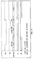
- Figs. 3 and 4 the access for such implementation is shown in Figs. 3 and 4 as correlated with the structure of Fig. 1.
- a row address is first provided using 'ras' (row address strobe), Figs. 1,3 and 4, as the control line.
- 'ras' row address strobe
- Figs. 1,3 and 4 the control line.
- the column address is presented over the same pins under the control of 'cas' signal.
- a syncronous ('PARAS') DRAM top level internal block diagram is shown in Fig. 5 for ease of explanation only.
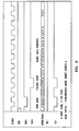
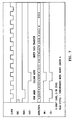
- a clock and clock enable signal is provided in such type of DRAM and the access for such an implementation is shown in Figs. 6 and 7 and in the context of the device of Fig.
- the 64M x 16 'PARAS' DRAMs can be dropped in place of 4M x 16, as they will be pin compatible. This contrasts with prevailing technology where a new board design and subsequent significant manufacturing related expenses must be incurred. Time to market is a major factor and will be seriously affected, since 4M x 4 existing DRAMs are not pin compatible with future 64M x 4. As stated earlier, moreover, the invention is capable of accomodating storage sizes 256 times larger for x 4 configuration of existing DRAMs and 65536 times for x 8 configuration of existing DRAMs with the comparable package size.
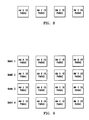
- the invention also provides much finer granularity than the existing sync or async DRAMs and consumes far lower numbers of components when multiple banks are used in the design. If, as an example, 4 separate banks of 4m x 64 are needed, Fig. 9, the based array of the invention would need only 16 devices, as shown. This compares well against the existing async or aync DRAM-based implementation, which will consume 64 components, as shown in Fig. 10.
- a column address counter is preferably incorporated in the invention to facilitate sequential access fast page mode and with faster access than the traditional async design; the invention, in all cases, providing increased address and data bandwidth and, where desired, resulting in substantially lower numbers of components.
- the system and technique of the invention are thus expected to be enormous useful for large numbers of applications and serving as a critical component for designs where space and power consumption are at a premium.
- the memory controller has different sequencing and timings, as before explained, than what traditional DRAM designers employ, with the multiplexer circuit used to multiplex the row and column address being of tristate type, Fig. 3, 4, 6 and 7, to allow for the data to reside on the same bus.
- the package size is kept comparable with current devices, but the number of data bits has increased significantly.
- the increased data bandwidth at each part results in significantly reduced number of parts required to meet the wider data bus size, and the package size is kept the same or nearly the same, but with the number of uniquely addressable locations increased significantly.
- a most significant advantage of 'PARAS' resides in the larger data bandwidth and higher potential density which have a significant impact on the system implementation, enabling reduced board "real estate", lower power consumption, reduced manufacturing cost, and a large range of drop-in pin compatibility.
Landscapes
- Engineering & Computer Science (AREA)
- Microelectronics & Electronic Packaging (AREA)
- Computer Hardware Design (AREA)
- Databases & Information Systems (AREA)
- Dram (AREA)
Applications Claiming Priority (2)
| Application Number | Priority Date | Filing Date | Title |
|---|---|---|---|
| US320058 | 1994-10-07 | ||
| US08/320,058 US5590078A (en) | 1994-10-07 | 1994-10-07 | Method of and apparatus for improved dynamic random access memory (DRAM) providing increased data bandwidth and addressing range for current DRAM devices and/or equivalent bandwidth and addressing range for smaller DRAM devices |
Publications (2)
| Publication Number | Publication Date |
|---|---|
| EP0706186A2 true EP0706186A2 (de) | 1996-04-10 |
| EP0706186A3 EP0706186A3 (de) | 1997-08-20 |
Family
ID=23244694
Family Applications (1)
| Application Number | Title | Priority Date | Filing Date |
|---|---|---|---|
| EP95307110A Withdrawn EP0706186A3 (de) | 1994-10-07 | 1995-10-06 | DRAM-Speicheranordnungen |
Country Status (8)
| Country | Link |
|---|---|
| US (1) | US5590078A (de) |
| EP (1) | EP0706186A3 (de) |
| JP (1) | JPH08315565A (de) |
| KR (1) | KR960015576A (de) |
| CN (1) | CN1152780A (de) |
| CA (1) | CA2159953A1 (de) |
| MX (1) | MX9504236A (de) |
| TW (1) | TW288202B (de) |
Cited By (1)
| Publication number | Priority date | Publication date | Assignee | Title |
|---|---|---|---|---|
| EP1472566A4 (de) * | 2002-02-08 | 2009-04-22 | Samsung Electronics Co Ltd | Flüssigkristallanzeige und ansteuerverfahren dafür und frame-speicher |
Families Citing this family (35)
| Publication number | Priority date | Publication date | Assignee | Title |
|---|---|---|---|---|
| US6525971B2 (en) | 1995-06-30 | 2003-02-25 | Micron Technology, Inc. | Distributed write data drivers for burst access memories |
| US5526320A (en) | 1994-12-23 | 1996-06-11 | Micron Technology Inc. | Burst EDO memory device |
| US6804760B2 (en) * | 1994-12-23 | 2004-10-12 | Micron Technology, Inc. | Method for determining a type of memory present in a system |
| US6035369A (en) | 1995-10-19 | 2000-03-07 | Rambus Inc. | Method and apparatus for providing a memory with write enable information |
| US6199142B1 (en) * | 1996-07-01 | 2001-03-06 | Sun Microsystems, Inc. | Processor/memory device with integrated CPU, main memory, and full width cache and associated method |
| US6031767A (en) * | 1996-09-18 | 2000-02-29 | International Business Machines Corporation | Integrated circuit I/O interface that uses excess data I/O pin bandwidth to input control signals or output status information |
| US6016537A (en) * | 1997-03-07 | 2000-01-18 | Advanced Micro Devices, Inc. | Method and apparatus for address multiplexing to support variable DRAM sizes |
| US6327640B1 (en) | 1997-03-07 | 2001-12-04 | Advanced Micro Devices, Inc. | Overlapping peripheral chip select space with DRAM on a microcontroller with an integrated DRAM controller |
| US6260101B1 (en) | 1997-03-07 | 2001-07-10 | Advanced Micro Devices, Inc. | Microcontroller having dedicated hardware for memory address space expansion supporting both static and dynamic memory devices |
| US6643165B2 (en) | 2001-07-25 | 2003-11-04 | Nantero, Inc. | Electromechanical memory having cell selection circuitry constructed with nanotube technology |
| US7566478B2 (en) | 2001-07-25 | 2009-07-28 | Nantero, Inc. | Methods of making carbon nanotube films, layers, fabrics, ribbons, elements and articles |
| US6924538B2 (en) | 2001-07-25 | 2005-08-02 | Nantero, Inc. | Devices having vertically-disposed nanofabric articles and methods of making the same |
| US6706402B2 (en) | 2001-07-25 | 2004-03-16 | Nantero, Inc. | Nanotube films and articles |
| US6911682B2 (en) | 2001-12-28 | 2005-06-28 | Nantero, Inc. | Electromechanical three-trace junction devices |
| US6835591B2 (en) | 2001-07-25 | 2004-12-28 | Nantero, Inc. | Methods of nanotube films and articles |
| US6574130B2 (en) | 2001-07-25 | 2003-06-03 | Nantero, Inc. | Hybrid circuit having nanotube electromechanical memory |
| US6919592B2 (en) | 2001-07-25 | 2005-07-19 | Nantero, Inc. | Electromechanical memory array using nanotube ribbons and method for making same |
| US7259410B2 (en) | 2001-07-25 | 2007-08-21 | Nantero, Inc. | Devices having horizontally-disposed nanofabric articles and methods of making the same |
| US6784028B2 (en) | 2001-12-28 | 2004-08-31 | Nantero, Inc. | Methods of making electromechanical three-trace junction devices |
| US7176505B2 (en) | 2001-12-28 | 2007-02-13 | Nantero, Inc. | Electromechanical three-trace junction devices |
| US7335395B2 (en) | 2002-04-23 | 2008-02-26 | Nantero, Inc. | Methods of using pre-formed nanotubes to make carbon nanotube films, layers, fabrics, ribbons, elements and articles |
| US7466160B2 (en) * | 2002-11-27 | 2008-12-16 | Inapac Technology, Inc. | Shared memory bus architecture for system with processor and memory units |
| US7560136B2 (en) | 2003-01-13 | 2009-07-14 | Nantero, Inc. | Methods of using thin metal layers to make carbon nanotube films, layers, fabrics, ribbons, elements and articles |
| CN100343822C (zh) * | 2003-10-27 | 2007-10-17 | 华为技术有限公司 | 地址复用逻辑实现与sdram兼容的方法 |
| CN100343823C (zh) * | 2003-10-27 | 2007-10-17 | 华为技术有限公司 | 地址复用逻辑兼容多种sdram的方法 |
| CN100343824C (zh) * | 2003-11-07 | 2007-10-17 | 华为技术有限公司 | 一种实现sdram兼容设计的方法 |
| KR101048380B1 (ko) * | 2005-05-21 | 2011-07-12 | 삼성전자주식회사 | 메모리 모듈 장치 |
| US7965530B2 (en) * | 2005-05-21 | 2011-06-21 | Samsung Electronics Co., Ltd. | Memory modules and memory systems having the same |
| US7804723B2 (en) | 2005-09-28 | 2010-09-28 | Hynix Semiconductor Inc. | Semiconductor memory device with signal aligning circuit |
| KR100719149B1 (ko) * | 2005-09-28 | 2007-05-18 | 주식회사 하이닉스반도체 | 신호 정렬 회로 및 이를 구비한 반도체 메모리 소자 |
| US7593271B2 (en) * | 2006-05-04 | 2009-09-22 | Rambus Inc. | Memory device including multiplexed inputs |
| US7466603B2 (en) * | 2006-10-03 | 2008-12-16 | Inapac Technology, Inc. | Memory accessing circuit system |
| US8462561B2 (en) * | 2011-08-03 | 2013-06-11 | Hamilton Sundstrand Corporation | System and method for interfacing burst mode devices and page mode devices |
| CN105788027B (zh) * | 2016-03-17 | 2019-12-17 | 中车株洲电力机车有限公司 | 一种事件记录装置及其记录方法 |
| CN111045965B (zh) * | 2019-10-25 | 2021-06-04 | 南京大学 | 一种多通道无冲突拆分的硬件实现方法及运行该方法的计算机设备与可读存储介质 |
Family Cites Families (4)
| Publication number | Priority date | Publication date | Assignee | Title |
|---|---|---|---|---|
| US4449207A (en) * | 1982-04-29 | 1984-05-15 | Intel Corporation | Byte-wide dynamic RAM with multiplexed internal buses |
| US5150328A (en) * | 1988-10-25 | 1992-09-22 | Internation Business Machines Corporation | Memory organization with arrays having an alternate data port facility |
| US5440749A (en) * | 1989-08-03 | 1995-08-08 | Nanotronics Corporation | High performance, low cost microprocessor architecture |
| US5430676A (en) * | 1993-06-02 | 1995-07-04 | Rambus, Inc. | Dynamic random access memory system |
-
1994
- 1994-10-07 US US08/320,058 patent/US5590078A/en not_active Expired - Lifetime
-
1995
- 1995-10-05 CA CA002159953A patent/CA2159953A1/en not_active Abandoned
- 1995-10-06 MX MX9504236A patent/MX9504236A/es unknown
- 1995-10-06 JP JP7260304A patent/JPH08315565A/ja active Pending
- 1995-10-06 KR KR1019950034257A patent/KR960015576A/ko not_active Ceased
- 1995-10-06 EP EP95307110A patent/EP0706186A3/de not_active Withdrawn
- 1995-10-09 CN CN95117951A patent/CN1152780A/zh active Pending
- 1995-11-10 TW TW084111950A patent/TW288202B/zh active
Cited By (1)
| Publication number | Priority date | Publication date | Assignee | Title |
|---|---|---|---|---|
| EP1472566A4 (de) * | 2002-02-08 | 2009-04-22 | Samsung Electronics Co Ltd | Flüssigkristallanzeige und ansteuerverfahren dafür und frame-speicher |
Also Published As
| Publication number | Publication date |
|---|---|
| CN1152780A (zh) | 1997-06-25 |
| KR960015576A (ko) | 1996-05-22 |
| EP0706186A3 (de) | 1997-08-20 |
| US5590078A (en) | 1996-12-31 |
| JPH08315565A (ja) | 1996-11-29 |
| MX9504236A (es) | 1997-04-30 |
| TW288202B (de) | 1996-10-11 |
| CA2159953A1 (en) | 1996-04-08 |
Similar Documents
| Publication | Publication Date | Title |
|---|---|---|
| US5590078A (en) | Method of and apparatus for improved dynamic random access memory (DRAM) providing increased data bandwidth and addressing range for current DRAM devices and/or equivalent bandwidth and addressing range for smaller DRAM devices | |
| US5604714A (en) | DRAM having multiple column address strobe operation | |
| US5901304A (en) | Emulating quasi-synchronous DRAM with asynchronous DRAM | |
| US5555528A (en) | Dynamic random access memory persistent page implemented as processor register sets | |
| US5506814A (en) | Video random access memory device and method implementing independent two WE nibble control | |
| US9218871B2 (en) | Semiconductor memory device, information processing system including the same, and controller | |
| JP2851503B2 (ja) | 集積回路記憶装置 | |
| US5966724A (en) | Synchronous memory device with dual page and burst mode operations | |
| US5394541A (en) | Programmable memory timing method and apparatus for programmably generating generic and then type specific memory timing signals | |
| US8369168B2 (en) | Devices and system providing reduced quantity of interconnections | |
| US20030217223A1 (en) | Combined command set | |
| JPH11265315A (ja) | 様々なdramバンクサイズと複数のインターリービング機構とをサポートする高速でコンパクトなアドレスビット経路指定機構 | |
| US5907518A (en) | Memory device with regulated power supply control | |
| JP2005517242A (ja) | アドレス空間、バスシステム、メモリコントローラ及びデバイスシステム | |
| US20070028027A1 (en) | Memory device and method having separate write data and read data buses | |
| Sato et al. | Fast Cycle RAM (FCRAM); a 20-ns random row access, pipe-lined operating DRAM | |
| US6888760B2 (en) | System and method for multiplexing data and data masking information on a data bus of a memory device | |
| WO2003007303A2 (en) | Memory device having different burst order addressing for read and write operations | |
| US6157990A (en) | Independent chip select for SRAM and DRAM in a multi-port RAM | |
| US5969997A (en) | Narrow data width DRAM with low latency page-hit operations | |
| US20020147883A1 (en) | System and method for increasing the speed of memories | |
| US5559749A (en) | Multi-bit block write in a random access memory | |
| US5761137A (en) | DRAM access system and method | |
| KR19980016197A (ko) | 반도체 메모리소자의 리프레시 제어회로 | |
| US6785190B1 (en) | Method for opening pages of memory with a single command |
Legal Events
| Date | Code | Title | Description |
|---|---|---|---|
| PUAI | Public reference made under article 153(3) epc to a published international application that has entered the european phase |
Free format text: ORIGINAL CODE: 0009012 |
|
| AK | Designated contracting states |
Kind code of ref document: A2 Designated state(s): DE FR GB IT NL SE |
|
| PUAL | Search report despatched |
Free format text: ORIGINAL CODE: 0009013 |
|
| AK | Designated contracting states |
Kind code of ref document: A3 Designated state(s): DE FR GB IT NL SE |
|
| 17P | Request for examination filed |
Effective date: 19980506 |
|
| 17Q | First examination report despatched |
Effective date: 19991011 |
|
| STAA | Information on the status of an ep patent application or granted ep patent |
Free format text: STATUS: THE APPLICATION HAS BEEN WITHDRAWN |
|
| 18W | Application withdrawn |
Withdrawal date: 20021107 |
|
| APAF | Appeal reference modified |
Free format text: ORIGINAL CODE: EPIDOSCREFNE |