EP0706054A2 - Comparateur de phase - Google Patents
Comparateur de phase Download PDFInfo
- Publication number
- EP0706054A2 EP0706054A2 EP95115746A EP95115746A EP0706054A2 EP 0706054 A2 EP0706054 A2 EP 0706054A2 EP 95115746 A EP95115746 A EP 95115746A EP 95115746 A EP95115746 A EP 95115746A EP 0706054 A2 EP0706054 A2 EP 0706054A2
- Authority
- EP
- European Patent Office
- Prior art keywords
- voltage
- phase
- voltages
- phase comparator
- checking
- Prior art date
- Legal status (The legal status is an assumption and is not a legal conclusion. Google has not performed a legal analysis and makes no representation as to the accuracy of the status listed.)
- Granted
Links
Images


Classifications
-
- G—PHYSICS
- G01—MEASURING; TESTING
- G01R—MEASURING ELECTRIC VARIABLES; MEASURING MAGNETIC VARIABLES
- G01R25/00—Arrangements for measuring phase angle between a voltage and a current or between voltages or currents
-
- G—PHYSICS
- G01—MEASURING; TESTING
- G01R—MEASURING ELECTRIC VARIABLES; MEASURING MAGNETIC VARIABLES
- G01R25/00—Arrangements for measuring phase angle between a voltage and a current or between voltages or currents
- G01R25/005—Circuits for comparing several input signals and for indicating the result of this comparison, e.g. equal, different, greater, smaller, or for passing one of the input signals as output signal
Definitions
- the innovation concerns a phase comparator.
- phase comparators are primarily used to test medium-voltage systems.
- Medium-voltage systems are systems that work with AC voltages between 1 and 52 kilovolts (kV). It is important to determine the operating status of such medium-voltage systems. To do this, it must be determined whether a certain phase of the AC voltage is present at all. Furthermore, the phase difference between two AC voltages tapped at different points is to be determined. Alternating voltages with a phase difference of up to 15 ° are still considered to be in phase. At AC voltages with phase differences of more than 60 ° are clearly phase inequality. In between there is a transition area.
- phase comparator In order to be able to work with manageable voltages during the measurements, partial voltages of the order of a few volts are tapped from the voltages by means of a capacitive voltage divider. These are then processed further (DIN VDE 0681 part 7). The phase comparator then provides "binary" displays in the form of "voltage present", “phases equal” or “phases not equal”. The displays can e.g. done by LEDs.
- phase comparator itself is certainly functional. A failure to report due to a malfunction of the phase comparator can have serious consequences.
- the innovation is based on the task of creating an improved phase comparator for the present or similar purposes.
- the innovation is based on the task of creating a phase comparator that is simple in structure and works reliably.
- the phase comparator according to the invention is characterized by means for generating a time cycle, zero point switch for determining at least three zero crossings of the AC voltages in relation to this time cycle, and means for determining the phase position of the AC voltage based on the time cycle from the respective zero crossings and means for determining the difference the phase positions determined in this way.
- the basic principle of the phase comparison according to the innovation is therefore the following: Three zero crossings are determined from each of the two AC voltages.
- the phase of each of the AC voltages with respect to the timing can be determined from the position of these zero crossings with respect to the timing.
- the difference between the phases determined in this way is then determined in the form of a corresponding number of time cycles.
- Each of the AC voltages can possibly be slightly offset from the zero line.
- the zero crossings then do not follow one another at exactly the same intervals. It is approximately the time interval between the first (rising) and the second (falling) zero crossing less than the time interval between the second (falling and third (rising) zero crossing. This indicates that the zero line of the measurement is up relative to the AC voltage If it is larger, it indicates that the zero line of the measurement is offset downwards relative to the AC voltage, and the greater the difference in time intervals, the greater the offset.
- the "means for determining the phase positions" therefore contain means for determining and taking into account a zero line offset of the alternating voltages from unequal time intervals of the zero crossings.
- the phase comparison it is preferably determined whether AC voltages of sufficient amplitude are present at the measuring points. This can be done by means of a threshold switch for each of the two AC voltages to which the AC voltage is applied Determination of the time interval during which the threshold value is exceeded by the respective AC voltage, and means for displaying whether the time interval falls below a predetermined limit value as an indication of the presence or absence of the AC voltage.
- the amplitude of the AC voltage is greater than the threshold value of the threshold switch, but only slightly exceeds this threshold value, then the AC voltage is only greater than the threshold value for a short time interval.
- This time interval is e.g. as the number of time cycles. If, on the other hand, the amplitude of the AC voltage is large compared to the threshold value of the threshold value switch, then the AC voltage is above the threshold value for practically the full half-period.
- a limit value time interval can now be specified: If the time interval during which the AC voltage exceeds the threshold value of the threshold value switch is shorter than this limit value time interval, this means: “No voltage”. If the time interval during which the AC voltage exceeds the threshold value of the threshold switch is longer than this limit value time interval, then this means: "voltage present". Here, too, the voltage measurement is traced back to a counting of time cycles.
- Means for checking the frequency equality of the two AC voltages are also preferably provided before the difference between the phases is determined. This ensures that the frequencies of the two AC voltages match each other with sufficient accuracy to enable a sensible phase measurement.
- the frequencies can be determined from the number of clock cycles in the interval between one zero crossing and the next but one.
- the frequency measurement is therefore also based on a count of Time clocks traced.
- the frequency comparison consists of a comparison of timing numbers.
- the means for checking the frequency equality, the means for determining the phase positions and the difference between the phase positions, the means for determining the zero line offset and the time interval determining and evaluating means can be formed by a microprocessor programmed for this purpose. Instead, e.g. a custom integrated circuit (ASIC) can be provided for these functions.
- ASIC custom integrated circuit
- the phase comparator can also contain self-checking means for checking the functionality of the phase comparator.
- These self-checking means can include means for checking the battery voltage of a battery feeding the phase comparator, means for checking display components by means of which results of the phase comparator can be displayed, e.g. of light-emitting diodes, and means for self-checking the phase measurement.
- the medium-voltage system contains an n-phase system, of which there are two lines 10 and 12, on which the high voltages to be tested are located. A processable partial voltage is tapped capacitively from each of the lines.
- a coupling electrode 14 with a dielectric 16 is used for this purpose. This coupling electrode 14 forms with the line, for example 12, and the dielectric between them a first capacitor 18.
- the first capacitor 18 forms with a second capacitor 20 a capacitive voltage divider between line 12 and ground.
- a partial voltage which is proportional to the voltage on the line 12 (or 10) and is essentially in phase therewith is tapped off at the capacitor 20.
- This partial voltage is applied via an interface 22 to a phase comparator 24 to be described.
- the phase comparator 24 has input impedances, which are represented here by a resistor 26.
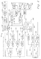
- FIG. 2 is a block diagram of the phase comparator 24.
- Two alternating voltages which are designated L and L x , can be applied to the phase comparator 24 via two inputs 30 and 32.
- the AC voltage L is connected in parallel via an input impedance 34 to a zero switch 36 and to a threshold switch 38.
- the output of the zero switch 36 is connected to an input 40 of a computer 42.
- the computer 42 is here of a microcontroller formed, which is commercially available under the name PIC 16C84.
- the signals obtained at the output of the threshold switch 38 are processed in a manner to be described by a signal conditioning circuit 44 and supply a signal at an input 46 of the computer 42.
- the signals from the zero point switch 36 are square-wave voltages and at least provide three consecutive zero crossings of the AC voltage L.
- the signal from the signal conditioning circuit 44 is a binary signal and signals whether an AC voltage L is present at all or not.
- the AC voltage L x is connected in parallel via an input impedance 48 to a zero point switch 50 and to a threshold value switch 52.
- the output of the zero point switch 50 is at an input 54 of the computer 42.
- the signals obtained at the output of the threshold switch 52 are also processed by a signal conditioning circuit 56 similar to the signal conditioning circuit 44 and provide a signal at an input 58 of the computer 42.
- the signals from the zero point switch 50 are again square-wave voltages and provide at least three consecutive zero crossings of the alternating voltage L x.
- the signal from the signal conditioning circuit 56 is a binary signal and signals whether an AC voltage L x is present.
- the computer 42 receives a clock pulse from a clock generator 60.
- the computer 42 controls its operating voltage, and the operating voltage of the phase comparator 24 from a power supply 62 via an ON / OFF circuit 64 and a control input 66.
- the voltage of the operating voltage is stabilized by a stabilizing circuit 68.
- Circuits 72 and 74 for port expansion are located at a port 70. This creates additional ports for the display device 76 and for a switch represented by block 78 for controlling the self-test.
- the self-test comprises a circuit 80 for battery testing, represented by a block, and the testing of the shields for the alternating voltages L and L x , which is represented by blocks 82 and 84, respectively.
- a "window comparator" 86 is also provided for the self-test to test the burning voltages of the light-emitting diodes used for the display.
- An external monitoring circuit (“watchdog") is located at a port 88 of the computer 42. Port 88 is also connected to circuit 92. Circuit 92 generates and feeds two amplifiers 94 and 96 with the higher voltage required for sine generation. Ports 98 and 100 provide pulse width signals, as will be described. From these pulse width signals, circuits 102 and 104 generate sinusoidal signals for the self-check of the phase comparison. These sinusoidal signals are amplified by amplifiers 94 and 96, respectively, and are connected to terminals 106 and 108.
- the circuit of the input impedances 34 and 48 is shown in Fig.3.
- a capacitive voltage divider consisting of capacitors 116 and 118 via a resistor 114.
- the resistor 114 protects the capacitors 116 and 118 from critical voltage rise speeds D u / D t and compensates for the phase-shifting component of the real part of the Parallel connection of capacitor 118, the Z-diodes 124 and 126 connected to each other and the measuring resistor 128.
- Between the terminals 110 and 112 lies the cable capacitance 120 of the connecting cable caused by the connection line.
- an overvoltage fuse 122 consisting of two Zener diodes 124 and 126 connected in series.
- An AC voltage dropping across a resistor 128 lies between two terminals 130 and 132. If the terminal 132 is not switched as a virtual zero point, it is connected to GND (device ground) , the terminal 130 is to be assigned a bias voltage via a resistor 134.
- the voltage at terminal 130 is connected via a resistor 134 (FIG. 4) to an input of an operational amplifier 136.
- the voltage present at the input of the operational amplifier is limited by diodes 138 and 140.
- the resistor 134 and the diodes 138 and 140 protect it Entrance of the Operational amplifier 136 against overvoltages that are greater than its supply voltage.
- a reference voltage from a reference voltage generator 142 is present at the second input of the operational amplifier 136.
- the voltage at terminal 130 is furthermore via a resistor 144 (FIG. 5) at an input of an operational amplifier 146.
- the voltage present at the input of operational amplifier 146 is also limited by diodes 148 and 150. Resistor 144 and diodes 148 and 150 again protect the input of operational amplifier 146 against voltages which are greater than the supply voltage.
- a reference voltage from a reference voltage generator 152 is present at the second input of the operational amplifier 146.
- the circuit of FIG. 4 represents the zero voltage switch 36 or the zero voltage switch 50 of FIG. 2.
- the circuit of FIG. 5 represents the threshold value switch 38 or the threshold value switch 52 of FIG.
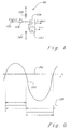
- FIG. 6 shows an AC voltage to be tested as a sinusoidal signal curve 154.
- the clock pulses 156 predefined by the clock generator 60 are schematically marked on the time axis t.
- the AC voltage is slightly offset from the zero line symbolized by the time axis (this offset can have a positive or a negative sign and is due to the component tolerances).
- the operational amplifier 136 turns this into a square wave voltage 158, as shown in the lower part of FIG. 6.
- the edges of the square wave voltage 158 define three zero crossings A, B and C of the AC voltage 154.
- the zero crossings are fed to the computer.
- the number of clock cycles 156 in the time intervals t 1 and t 2 are counted. From the differences in the number of clock cycles 156, computer 42 determines the zero line offset and the correct phase of the AC voltage with respect to the clock cycle.
- the reference voltage from the reference voltage generator 142 is used here to carry out an at least approximate zero line adjustment.
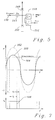
- FIG. 7 illustrates how a signal is obtained using the threshold switch from FIG. 5 for whether an AC voltage is present at all or not.
- 160 denotes the signal curve of an alternating voltage present at the operational amplifier 146 of relatively low amplitude.
- 162 denotes the signal curve of an alternating voltage present at the operational amplifier 146 of a relatively large amplitude.
- the threshold value switch 38 with the operational amplifier 146 and the reference voltage generator 152 defines a threshold value 164. The two AC voltages exceed the threshold value in a middle area around the maximum. In the case of the AC voltage 160, the threshold value 164 is exceeded by the signal curve in a time interval t 3.
- the threshold 164 is exceeded by the signal curve in a time interval tinter that is greater than the time interval t3.
- the operational amplifier 146 supplies square-wave signals like the square-wave signal 166. These square-wave signals 166 are applied to the computer 42.
- the computer 42 determines the length of the square-wave signals 166 by counting the clock pulses of the clock generator 60 which appear during the presence of the square-wave signals 166. If the number of the time cycles counted in this way is less than a certain limit value, the computer then signals: "No voltage". If, on the other hand, the number of counted clock cycles is greater than the limit value, "voltage present" is signaled.
- the arrangement of FIG. 8 can also be used to relieve the computer 42 of the task of counting the clock cycles.
- the exceeding or falling below the limit value is determined analogously, and accordingly a single binary signal is generated which is applied to the computer 42.
- a threshold switch of the type shown in FIG. 5 is also provided. Corresponding parts are given the same reference numerals in FIG. 8 as in FIG. 5.
- the output signal of the threshold switch is a sequence of pulses, the pulse width of which depends on the amplitude of the AC voltage. These pulses are now filtered by a filter 168 and rectified by a rectifier 170. This produces a DC voltage, the magnitude of which depends on the pulse width of the pulses.
- the DC voltage is connected to a Schmitt trigger 172.
- the Schmitt trigger 172 goes into a first switching state, which signals the presence of an AC voltage, when the DC voltage exceeds a certain limit value.
- the Schmitt trigger 172 goes into a second switching state, which signals the absence of an AC voltage, when the DC voltage falls below the limit value.
- the binary signal (1 or 0) thus obtained from the Schmitt trigger is also connected to the computer 42.
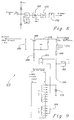
- FIG. 9 shows the ON / OFF circuit 64 from FIG. 2 in detail.
- the phase comparator 24 is switched on and off by a button 174. If the phase comparator 24 is switched on, it must be switched off by pressing a key. If the phase comparator 24 is switched off, the key press must bring about a switch-on.
- the supply voltage from the power supply (battery) 62 on line 176 outputs a partial voltage determined by a Zener diode 178 via a resistor 180 to a monostable multivibrator 182.
- the monostable multivibrator 182 controls, via an OR gate 184 and a resistor 186, a series transistor 188, which has its emitter-collector path in line 176 and connects the power supply 62 (FIG. 2) to the port 66 of the computer 42 .
- the pulse from the monostable multivibrator 182 therefore passes through the OR gate 184.
- the computer 42 is energized.
- the computer 42 when it is live, supplies a signal at an output 194 which is connected to the second input of the OR gate. After resetting the monostable multivibrator, the series transistor is kept conductive via output 194 and OR gate 184. The computer 42 remains connected to the power supply 62.
- the states of the voltages to be tested are "binary” as “voltage present” or “voltage not present”, “voltages in phase” or “voltages out of phase” as well as “incorrect measurements” or “fault” by means of LEDs 196, 198, 200, 202, 204, 206 and 208 are displayed.
- Each of the light-emitting diodes 196 to 208 is connected to the supply voltage via a resistor 210, as will be described with reference to the light-emitting diode 196.
- the supply voltage is supplied via a line 212.
- the emitter-collector path of a transistor 214 is located in series with the light-emitting diode 196.
- the emitter of the transistor 214 is connected to GND (device ground).
- the base of the transistor is connected to a wire of a bus 218 via a resistor 216, via which control signals from the computer 42 are applied to the display device 76.
- the base of transistor 214 is connected to GND (device ground) via a capacitor 220.
- the voltages falling across the light-emitting diodes 196 are tapped off for testing purposes via the wires of a cable 222.
- FIG. 11 shows a "window comparator” 86 (FIG. 2) for checking the burning voltages of the light-emitting diodes 196 to 208 (FIG. 10).
- the window comparator 86 is controlled by the computer 42. It checks whether the burning voltages of the LEDs are within the specified "window”.
- the remote window comparator 86 contains electronic switches 224, 226, 228, 230, 232, 234 and 236, which are successively activated by the computer via a bus 238 in the course of the test program. Each of the electronic switches 224 to 236 connects one wire of the cable 222 (FIG. 10) to a comparator arrangement 240.
- the comparator arrangement 240 contains two comparators 242 and 244.
- the respective switched-on operating voltage is applied to the "lower” input of the comparator 242 and to the "upper” input of the comparator 244.
- a voltage divider with three resistors 246, 248 and 250 between the Supply voltage and GND (device ground) provides an upper reference voltage at a tap 252 and a lower reference voltage at a tap 254.
- the upper reference voltage is at the "upper” input of the comparator 242.
- the lower reference voltage is at the "lower” input of the Comparator 244.
- Comparator 242 switches and delivers an output signal when the operating voltage at the lower input, which is switched through via the respective switch 224 to 236, is less than the upper reference voltage at tap 252.
- the comparator 244 switches and supplies an output signal when the operating voltage that is switched through is greater than the lower reference voltage at the tap 254.
- the outputs of the comparators 242 and 244 are linked by an AND gate 256.
- the AND gate 256 delivers a "logic 1" signal to the computer 42 via its output 258 when the operating voltage applied is in a "window” specified by the upper and lower reference voltages.
- the burning voltages of the LEDs vary depending on the color of the LED. In the present case, the light-emitting diodes 196, 200 and 204 have different colors than the other light-emitting diodes and a lower operating voltage.
- control signals of the computer 42 for the assigned electronic switches 224, 228 and 232 are linked via an OR gate 260.
- the output of the OR gate 260 controls another electronic switch 262.
- the switch 262 then becomes conductive and places a resistor 264 in parallel with the resistor 250 of the voltage divider.
- the upper and lower reference voltages are thus pulled down and the window is adapted to the lower operating voltage of the LEDs 196, 200 and 204.
- FIG. 12 shows in detail the formation of the sinusoidal test voltages for testing the phase comparison means.
- the computer 42 delivers pulse sequences via the ports 98 and 100 (FIG. 2) and a cable 266, in which the pulse width changes sinusoidally.
- the pulse trains are smoothed by filters.
- Each of the filters consists of a resistor 268 or 270 and a capacitor 272 or 274.
- the smoothed, sinusoidal voltages are amplified by the amplifiers 94 and 96 (see also FIG. 2).
- Amplifiers 94 and 96 provide sinusoidal test voltages with known phase relationships at terminals 106 and 108, respectively.
- Fig. 13 shows the circuit 80 for battery testing.
- a partial voltage of the battery voltage present at a terminal 276 is compared on a comparator 278 with a voltage of a reference voltage generator 280.
- the reference voltage generator 280 is fed by the supply voltage.
- the partial voltage of the battery voltage is tapped at a voltage divider with resistors 282 and 284.
- the supply voltage is switched off when the phase comparator is not in operation. However, current would flow continuously via the voltage divider 282, 284 and load the battery. For this reason, the emitter-collector path of a transistor 286 is connected in series with the voltage divider 282, 284.
- the base of this transistor 286 is connected to a voltage divider with a resistor 288 and 290 between the terminals 276 and GND (device ground).
- transistor 292 In series with resistor 290 there is still the emitter-collector path of a transistor 292.
- the base of transistor 292 is connected to a voltage section with resistors 294 and 296 connected between the supply voltage and GND (device ground). As a result, transistor 292 is blocked when the supply voltage is switched off , and this also turns off transistor 286.
- FIG. 14 illustrates the switch-on process.
- a rectangle 298 "ON / OFF" symbolizes the actuation of the button 174 in FIG. 9.
- a rhombus 300 corresponds to the test whether a switch-on or a switch-off takes place.
- the signal at port 194 is set to "logical 1" according to rectangle 302. This initiates a return to the main program, as represented by oval 304.
- the signal at port 194 is reset to "logic 0". This is represented by rectangle 306. There is no further activity, as indicated by the rectangle 308 "waiting".
- the main program first controls a self-test of the phase comparator.
- the battery, the shielding, the LEDs of the display and the voltage and phase measurement are checked one after the other.
- a flowchart of this part of the main program is shown in FIGS. 15, 16 and 17, which represent successive sections of the flowchart.
- the ON / OFF circuit according to FIG. 14 is initially shown as a rectangle 310, it being assumed that the system has been switched on.
- a self-check flag is then set.
- This self-test indicator signals to the device that a self-test program is running and, for example, that no display should take place.
- the setting of the self-check indicator is represented by a rectangle 312.
- the battery is then selected for the battery test according to Fig. 13.
- the output of the comparator 278 in Fig. 13 is queried. This is represented by a rectangle 314.
- the battery test switches on a waiting time of 10 ms to take transients into account. This is represented by a rectangle 316. After this time, the battery test is evaluated. This is represented by a rectangle 318.
- the means for checking the shielding of the lines for the two alternating voltages L and L x are then selected, which are denoted by 82 and 84 in FIG.
- Such means for testing shielding are known per se and are therefore not described in detail here.
- This selection of the means for testing the shielding is represented by a rectangle 334.
- a delay is activated before the test is evaluated in order to take transients into account. This is represented by a rectangle 336.
- the test result is stored in the EEPROM. This is represented by a rectangle 342. If the shielding is correct (yes), this test result is also saved in the EEPROM. This is represented by loop 344.
- test program continues with the flow chart of FIG. 16, as indicated by the triangle "1".
- FIGS. 10 and 11 show the testing of the light-emitting diodes 196 to 208 according to FIGS. 10 and 11.
- the LED test is "selected", i.e. the configuration of inputs and outputs required for this is produced in the circuit of FIGS. 10 and 11. This is represented by a rectangle 344.
- the light emitting diodes 196 to 208 are identified by a consecutive number from “1" to "7” and are controlled in succession by the computer 42 via the bus 238 and the switches 224 to 236 in this order.
- the program works with two variables which are present in two counters of the computer 42.
- the first variable “LED” is the light emitting diode which is switched on by the computer 42 during the light emitting diode test.
- the second variable “LED test " indicates the light-emitting diode, the burning voltage of which is to be checked in each case with the window comparator 86. If the display device 76 is intact, only the light-emitting diode that is switched on should be burning, while no burning voltage drops on the other light-emitting diodes.
- a bit pattern is then stored, which is 0000001 when the display device is intact: the switched on light-emitting diode 196 burns and supplies a burning voltage within the window specified by the window comparator 86, the other light-emitting diodes 198 to 208 do not burn.
- the bit pattern (eg 0000001) obtained from the tests of the window comparator 86 is now replaced with a bit pattern in which a position corresponding to the switched-on light-emitting diode, here the light-emitting diode 196) is represented by a "1" and the remaining positions by a "0" are subject to an exclusive OR operation.
- variable LED ie the number of the LED to be switched on
- the variable LED is then increased by 1. This is represented by a rectangle 368. If the exclusive OR operation 362 is not> 0 (no), then the flow diagram goes directly to the rectangle 368 via a loop 370.
- the next test is directed to whether the variable LED is greater than the total number of light emitting diodes after the increase by 1. If this is not the case (no), then a loop 374 leads back to the rectangle 348 "delete display”. The LED 196 is extinguished. The next light-emitting diode 198 is now switched on, which corresponds to the LED number increased by 1. Then the test procedure for all light-emitting diodes runs again from light-emitting diode 196 (LED test number "1") via light-emitting diode 198 to light-emitting diode 208.
- the phase measurement is self-checked.
- two AC voltages with a defined relative phase position are generated.
- the phase positions of these AC voltages are determined in the manner described at the beginning with reference to FIGS. 4 and 6. It is checked whether the phase positions determined in this way match the phase positions of the AC voltages generated for the test.
- the values of the AC voltage are stored in a memory as a table. The values are called up in succession by "pointer" at a fixed time and switched to two channels. The pointers can call up the values synchronously. In this case, two in-phase AC voltages are generated.
- the pointers can also call up the values with an offset, that is, figuratively speaking, each on different "rows" of the "table".
- two alternating voltages that are phase-shifted with respect to one another are generated.
- the values in the value table called up in a given time cycle are converted into pulses of corresponding duration (pulse duration modulation).
- pulse duration modulation This results in pulse sequences with pulses of different widths, corresponding to the course of the AC voltage to be generated.
- These pulse trains are filtered and supply AC voltages with the signal curve corresponding to the table.
- This signal curve is usually sinusoidal. However, e.g. sawtooth or triangular waveforms are generated.
- Fig.17 the pulse duration modulation (PDM) is "selected".
- the supply voltage for amplifiers 94 and 94 (Fig. 12) is applied and outputs 98 and 100 activated. That is through a rectangle 378 is shown.
- the "pointers" for the two AC voltages L 1 and L x to be generated are set to 0 °. This is represented by the rectangles 380 and 382 in FIG.
- the subroutine "PDM pre-run” represented by rectangle 384 in FIG. 17 runs.
- This subroutine is shown in Fig. 18.
- the subroutine contains a query "PDM L1 >0?". This is represented by a 388 rhombus.
- PDM L1 is the value for L 1 stored in the table.
- a time counter is set to the maximum possible pulse duration "MaxPDM".
- This maximum possible pulse duration can be, for example, 255 clock cycles of the clock generator 60 (FIG. 2).
- a rectangle 400 represents the setting of the time counter to the maximum possible pulse duration. This time counter is then incrementally counted down. "Time” means the counter reading of the time counter. This counter reading is reduced by 1 on the next cycle. This is represented by a rectangle 402.
- a pulse with a constant level is generated at the outputs 98 and 100, the duration of the pulse being determined in each case by the digitally stored and read out value PDM L1 or PDM Lx . All the values in the table are now displayed one after the other as impulses variable width implemented. The leading edges of the pulses are equally spaced from one another. The duration of each pulse depends on the respective stored value PDM L1 or PDM Lx . In this way, several cycles are generated from the AC voltages.
- Fig. 19 This is shown in Fig. 19 as a flow chart.
- the subroutine of FIG. 18 is interrupted at fixed time intervals which are set by a timer and are somewhat longer than the maximum possible pulse duration. It is first checked whether the interruption is actually caused by the timer. This is represented by a rhombus 416. If this is not the case (no), the interruption has other causes. This is represented by a rectangle 418. In this case, loop 420 is used to return to the subroutine of FIG. 18. If the interruption is due to the timer (yes), the "pointers" switch to the next line in the table of stored signal values. This is represented by the rectangles 422 and 424 for the two sets of values PDM L1 and PDM Lx . It is checked whether the PDM L1 value then obtained is greater than the maximum possible pulse duration MaxPDM.
- a rhombus 426 If this is the case (yes), the value for PDM L1 is set to 0. A check is then carried out in the same way as to whether the PDM Lx value is greater than the maximum possible pulse duration. This is represented by a rhombus 428. If this is the case (yes), the value for PDM Lx is set to 0. This is represented by a rectangle 430. In both cases, the values for PDM L1 and PDM Lx are then replaced in the subroutine of FIG. 18 by the current values formed according to FIG. 19. This is represented by a rectangle 432 in FIG. 19. The program then returns to the subroutine of Fig. 18. This interruption and The pointers advance in the fixed cycle of the timer.
- This query is represented by a rhombus 434. If this is not the case (no), the flowchart jumps back to the start via a loop 436, namely to the rhombus 388. Then the entire subroutine is run through again. If the answer is affirmative (yes), the program proceeds to the measurement in the course of the self-test. This is represented by a rectangle 438 in FIG. 18.
- the program described delivers pulse sequences with a fixed frequency, the pulse widths changing in accordance with the digitally stored values in the table.
- the pulse duration modulated signals thus obtained are smoothed by filters 268, 272 or 270, 274 and amplified by amplifiers. There are alternating voltages with a predetermined phase relationship.
- phase relationships of the alternating voltages thus generated for test purposes are measured in the manner of FIGS. 4 and 6 and compared with the predetermined phase relationship.
- the results obtained are evaluated. This is represented by a rectangle 440 in FIG.
- a rhombus 442 in FIG. 17 symbolizes an inquiry as to whether the self-test showed that the means for the phase measurement are working properly. If this is not the case (no), an error indicator is set. This is represented by a rectangle 444. The positive or negative result is saved. This is represented by a rectangle 446. Finally, it is examined whether the error flag is set to "0". This is represented by a rhombus 448. If there was an error, that is it Error indicator not "0" (no), then the phase comparator is switched off. This is represented by a rectangle 450. If the error flag is "0" (yes), a self-check flag is set to "0". This is represented by a rectangle 452. Then the measurement can begin.
- the measurement is carried out with the same means for the internally generated alternating voltages as for the voltages to be tested.
- the three zero crossings A, B and C of the voltages are determined.
- the times A, B and C are set in relation to the clock of the clock generator 60.
- the periods may not differ from each other by more than 10%. It must T L1 / T Lx ⁇ 1 be. If this is not the case, an error indicator is set. If the periods and thus the frequencies of the two AC voltages match within the specified tolerances, the zero line offset is corrected.
- the zero point switch 36 for the AC voltage L 1 switches exactly at 0 volts, ie switches when the voltage L 1> 0, the zero point switch 52 for the AC voltage L x only switches when L x > 2 volts, then would be at exactly in-phase alternating voltages a phase shift are displayed.
- the shifting of the zero line means that the time intervals of the zero crossings become unequal in the generated square wave voltage, as shown in FIG.
- phase angle ⁇ 2 (A L1 - A Lx ) 360 ° / [(C L1 - A L1 ) + (C Lx - A Lx )].
- phase angle results from the difference between the times of the first zero crossings of the two voltages, divided by the mean value of the period lengths. This ratio is multiplied by 360 °.
- phase angle calculated in this way is less than 45 °, "Phase equal” is displayed. Otherwise, “Phase not equal” is displayed.
- the self-test ie when the self-test flag (312 of Fig. 15) is set, is the result of this test is not indicated by the display 76 (Fig. 2).
- Sp-L1 is a binary signal, from which, according to FIG. 7, the presence or absence of the AC voltage L 1 is inferred. This is the output of a comparator that compares the time, for example t 1 with a reference value.
- Sp-Lx is the corresponding signal for the AC voltage L x .
- Ph-L1 is the signal of the zero point switch 36 at the input 40 of the computer 42.
- Ph-Lx is the signal of the zero point switch 50 at the input 54 of the computer 42.
- the second column of the table shows changes in these various signals, eg from “logical 0" to "logical 1" (0-1).
- the third column indicates the conditions under which the changes take place, for example whether the measurement is running at the time the signal changes or not.
- the fourth column shows the action resulting from the signal change and the "condition", eg "Start measurement L x , save time A Lx ".
- the signals Sp-L1 and Sp-Lx according to rows 1 and 4 of the table change from 0 to 1, then this means that the voltages L 1 and L x are present. Then the measurement of L1 or L x can take place. If, on the other hand, the signals Sp-L1 and Sp-Lx change from 1 to 0 according to lines 2, 3 and 5, 6, the actions to be derived from them depend on the "conditions”. If the measurement is not yet running, the measurement will be affected AC voltage "forbidden", not even initiated. The measurement of an alternating voltage that is not present cannot give meaningful results. If the transition from 1 to 0 occurs while the measurement is running, the measurement according to lines 3 and 6 of the table must be stopped completely. Then, as indicated in the last line of the table, there is an error.
- the data stored in this way are processed in the manner described above to produce an advertisement.
- the results of the measurement are displayed by the light-emitting diodes 196 to 208, in contrast to the results which are obtained in the self-test.
- the processing of the data in the measurement of the external voltage is necessarily carried out by the same means and programs by which the processing of the internally generated AC voltages takes place.
- the internally generated AC voltages are further generated and processed according to the relationships above. If there is data on the external AC voltages to be tested, the program is interrupted.
- the test program is interrupted and the arithmetic operations are carried out with the data A, B and C of the external AC voltages. Then the test program continues at the same point.
- the generation and measurement of the internal AC voltages is terminated.
- Fig. 21 corresponds essentially to Fig. 18 already discussed. Comparable elements of the flow chart are provided with the same reference numerals as there.
- time 0
- rhombus 454 the flowchart is returned to the start of the program by a loop 456 such as loop 436 of FIG. 18.
- the answer is "yes”, it is checked whether there are measurement errors. This is represented by a 458 rhombus. If there are measurement errors (Yes), an error is registered. This is represented by a rectangle 460. If no measurement error is found (no), the measurement is evaluated. This is represented in FIG. 21 by a rectangle 462.
Applications Claiming Priority (2)
| Application Number | Priority Date | Filing Date | Title |
|---|---|---|---|
| DE4435905 | 1994-10-07 | ||
| DE4435905A DE4435905A1 (de) | 1994-10-07 | 1994-10-07 | Phasenvergleicher |
Publications (3)
| Publication Number | Publication Date |
|---|---|
| EP0706054A2 true EP0706054A2 (fr) | 1996-04-10 |
| EP0706054A3 EP0706054A3 (fr) | 1997-01-29 |
| EP0706054B1 EP0706054B1 (fr) | 1998-12-30 |
Family
ID=6530228
Family Applications (1)
| Application Number | Title | Priority Date | Filing Date |
|---|---|---|---|
| EP95115746A Revoked EP0706054B1 (fr) | 1994-10-07 | 1995-10-06 | Comparateur de phase |
Country Status (4)
| Country | Link |
|---|---|
| EP (1) | EP0706054B1 (fr) |
| AT (1) | ATE175278T1 (fr) |
| DE (2) | DE4435905A1 (fr) |
| DK (1) | DK0706054T3 (fr) |
Families Citing this family (1)
| Publication number | Priority date | Publication date | Assignee | Title |
|---|---|---|---|---|
| GB2618371A (en) * | 2022-05-05 | 2023-11-08 | Tdk Lambda Uk Ltd | Switch controller circuit and method for controlling switching |
Family Cites Families (9)
| Publication number | Priority date | Publication date | Assignee | Title |
|---|---|---|---|---|
| US3735250A (en) * | 1970-07-08 | 1973-05-22 | Shibaura Electric Comp | Fault detecting apparatus for a capacitor type potential divider having an amplifier |
| US3836854A (en) * | 1973-07-02 | 1974-09-17 | Lorain Prod Corp | Alarm circuit for monitoring the amplitude of a-c voltages |
| DE2727800B2 (de) * | 1977-06-21 | 1979-08-02 | Vogel & Halke, 2000 Hamburg | Schaltungsanordnung zum Betrieb und zur Funktionsfehlerüberwachung für LED-Anzeigen |
| SU779903A1 (ru) * | 1978-04-04 | 1980-11-15 | Омский Институт Инженеров Железнодорожного Транспорта | Цифровой фазометр |
| DE3348056C2 (fr) * | 1982-10-06 | 1987-10-29 | Takeda Riken Kogyo K.K., Tokio/Tokyo, Jp | |
| DE3407311A1 (de) * | 1984-02-24 | 1985-08-29 | Siemens AG, 1000 Berlin und 8000 München | Schaltungsanordnung zur ueberwachung einer spannung |
| DE3502638A1 (de) * | 1985-01-26 | 1986-07-31 | MWB Messwandler-Bau AG, 8600 Bamberg | Verfahren, schaltung und einrichtung zur beseitigung der gleichspannungskomponente eines kapazitiven wechselspannungsteilers |
| DE4221202A1 (de) * | 1992-06-27 | 1994-01-05 | Hermann Berger | Verfahren und Vorrichtung zur optischen Anzeige von Meßwerten |
| US5378979A (en) * | 1992-11-25 | 1995-01-03 | Allen-Bradley Company, Inc. | Method and apparatus for efficiently computing symmetric sequence signals in a three phase power system |
-
1994
- 1994-10-07 DE DE4435905A patent/DE4435905A1/de not_active Withdrawn
-
1995
- 1995-10-06 DE DE59504675T patent/DE59504675D1/de not_active Expired - Fee Related
- 1995-10-06 EP EP95115746A patent/EP0706054B1/fr not_active Revoked
- 1995-10-06 AT AT95115746T patent/ATE175278T1/de not_active IP Right Cessation
- 1995-10-06 DK DK95115746T patent/DK0706054T3/da active
Non-Patent Citations (1)
| Title |
|---|
| None |
Also Published As
| Publication number | Publication date |
|---|---|
| DK0706054T3 (da) | 1999-08-30 |
| DE59504675D1 (de) | 1999-02-11 |
| EP0706054B1 (fr) | 1998-12-30 |
| ATE175278T1 (de) | 1999-01-15 |
| EP0706054A3 (fr) | 1997-01-29 |
| DE4435905A1 (de) | 1996-04-11 |
Similar Documents
| Publication | Publication Date | Title |
|---|---|---|
| DE2727201A1 (de) | Beruehrungssteuertastenschaltung | |
| DE3502638A1 (de) | Verfahren, schaltung und einrichtung zur beseitigung der gleichspannungskomponente eines kapazitiven wechselspannungsteilers | |
| EP1900088B1 (fr) | Dispositif circuit pour determiner les passages par zero d'une tension alternative | |
| EP0134050B1 (fr) | Circuit pour le fonctionnement de lampes de décharge à gaz à haute pression | |
| DE4421906C2 (de) | Verfahren und Schaltungsanordnung zur Messung des Widerstandes eines Widerstandssensors | |
| DE2942134A1 (de) | Auswerteschaltung fuer einen induktivgeber | |
| DE3522586C2 (fr) | ||
| EP0706054B1 (fr) | Comparateur de phase | |
| DE2919152C2 (de) | Schaltungsanordnung zur Messung der Drehzahl einer Maschine | |
| DE2722581C3 (de) | Schaltungsanordnung zur Signalaufbereitung von Ausgangssignalen eines Feldplattengebers bei Raddrehzahlgebern von Fahrzeugen | |
| DE2602029A1 (de) | Ueberwachungsvorrichtung fuer fehlerhafte nadeln an laufenden wirk- und strickmaschinen | |
| DE19632457C1 (de) | Schaltungsanordnung zur Überwachung eines Sensors | |
| DE19843678A1 (de) | Verfahren zur Bereitstellung eines Ausgangssignals mit einem gewünschten Wert einer Kenngröße am Ausgang eines Schaltnetzteils und Schaltung zur Durchführung des Verfahrens | |
| DE1648587A1 (de) | Eichvorrichtung fuer elektronische Textilfaser-UEberwachungsanlage | |
| EP0066681A1 (fr) | Procédé pour mesurer une quantité correspondant au rapport cyclique d'un signal électrique périodique rectangulaire et procédé pour mesurer l'angle de phase entre deux signaux électriques périodiques rectangulaires en quadrature et dispositifs pour l'application desdits procédés | |
| DE3509682C2 (fr) | ||
| EP3783317A1 (fr) | Dispositif capteur à synchronisation d'un signal de capteur sur un signal d'interrogation | |
| DE2815089C2 (de) | Schaltungsanordnung zur Überwachung des Quadrats eines Effektivwertes eines periodischen Signals | |
| DE3813269A1 (de) | Netzueberwachungsschaltung | |
| DE2554223C3 (de) | Steuereinrichtung zur Aufrechterhaltung der Stabilität eines Wechselrichters | |
| DE2547746A1 (de) | Vorrichtung mit einer messwertgeber-einheit zur erzeugung einer folge von spannungswerten und einer mittelwertbildungs-einheit | |
| EP0053602B1 (fr) | Dispositif pour la génération d'une impulsion | |
| DE3616059C2 (fr) | ||
| DE1516242C3 (de) | Phasenvergleicheinrichtung | |
| DE1900260C3 (de) | Ortsveränderungsmeßvorrichtung |
Legal Events
| Date | Code | Title | Description |
|---|---|---|---|
| PUAI | Public reference made under article 153(3) epc to a published international application that has entered the european phase |
Free format text: ORIGINAL CODE: 0009012 |
|
| AK | Designated contracting states |
Kind code of ref document: A2 Designated state(s): AT BE CH DE DK FR GB IT LI NL SE |
|
| PUAL | Search report despatched |
Free format text: ORIGINAL CODE: 0009013 |
|
| AK | Designated contracting states |
Kind code of ref document: A3 Designated state(s): AT BE CH DE DK FR GB IT LI NL SE |
|
| 17P | Request for examination filed |
Effective date: 19970121 |
|
| 17Q | First examination report despatched |
Effective date: 19971106 |
|
| GRAG | Despatch of communication of intention to grant |
Free format text: ORIGINAL CODE: EPIDOS AGRA |
|
| GRAG | Despatch of communication of intention to grant |
Free format text: ORIGINAL CODE: EPIDOS AGRA |
|
| GRAH | Despatch of communication of intention to grant a patent |
Free format text: ORIGINAL CODE: EPIDOS IGRA |
|
| GRAH | Despatch of communication of intention to grant a patent |
Free format text: ORIGINAL CODE: EPIDOS IGRA |
|
| GRAA | (expected) grant |
Free format text: ORIGINAL CODE: 0009210 |
|
| AK | Designated contracting states |
Kind code of ref document: B1 Designated state(s): AT BE CH DE DK FR GB IT LI NL SE |
|
| REF | Corresponds to: |
Ref document number: 175278 Country of ref document: AT Date of ref document: 19990115 Kind code of ref document: T |
|
| REG | Reference to a national code |
Ref country code: CH Ref legal event code: EP |
|
| GBT | Gb: translation of ep patent filed (gb section 77(6)(a)/1977) |
Effective date: 19990118 |
|
| REF | Corresponds to: |
Ref document number: 59504675 Country of ref document: DE Date of ref document: 19990211 |
|
| ET | Fr: translation filed | ||
| REG | Reference to a national code |
Ref country code: CH Ref legal event code: NV Representative=s name: TROESCH SCHEIDEGGER WERNER AG |
|
| ITF | It: translation for a ep patent filed |
Owner name: STUDIO JAUMANN P. & C. S.N.C. |
|
| REG | Reference to a national code |
Ref country code: DK Ref legal event code: T3 |
|
| PLBQ | Unpublished change to opponent data |
Free format text: ORIGINAL CODE: EPIDOS OPPO |
|
| PLBI | Opposition filed |
Free format text: ORIGINAL CODE: 0009260 |
|
| 26 | Opposition filed |
Opponent name: DIPL. ING. H. HORSTMANN GMBH Effective date: 19990902 |
|
| PLBF | Reply of patent proprietor to notice(s) of opposition |
Free format text: ORIGINAL CODE: EPIDOS OBSO |
|
| PLBF | Reply of patent proprietor to notice(s) of opposition |
Free format text: ORIGINAL CODE: EPIDOS OBSO |
|
| NLR1 | Nl: opposition has been filed with the epo |
Opponent name: DIPL. ING. H. HORSTMANN GMBH |
|
| RDAH | Patent revoked |
Free format text: ORIGINAL CODE: EPIDOS REVO |
|
| APAC | Appeal dossier modified |
Free format text: ORIGINAL CODE: EPIDOS NOAPO |
|
| APAE | Appeal reference modified |
Free format text: ORIGINAL CODE: EPIDOS REFNO |
|
| APAC | Appeal dossier modified |
Free format text: ORIGINAL CODE: EPIDOS NOAPO |
|
| REG | Reference to a national code |
Ref country code: GB Ref legal event code: IF02 |
|
| PGFP | Annual fee paid to national office [announced via postgrant information from national office to epo] |
Ref country code: BE Payment date: 20030825 Year of fee payment: 9 |
|
| PGFP | Annual fee paid to national office [announced via postgrant information from national office to epo] |
Ref country code: FR Payment date: 20030826 Year of fee payment: 9 |
|
| PGFP | Annual fee paid to national office [announced via postgrant information from national office to epo] |
Ref country code: SE Payment date: 20030903 Year of fee payment: 9 |
|
| PGFP | Annual fee paid to national office [announced via postgrant information from national office to epo] |
Ref country code: GB Payment date: 20030923 Year of fee payment: 9 |
|
| PGFP | Annual fee paid to national office [announced via postgrant information from national office to epo] |
Ref country code: DK Payment date: 20031003 Year of fee payment: 9 |
|
| PGFP | Annual fee paid to national office [announced via postgrant information from national office to epo] |
Ref country code: AT Payment date: 20031014 Year of fee payment: 9 |
|
| PGFP | Annual fee paid to national office [announced via postgrant information from national office to epo] |
Ref country code: DE Payment date: 20031017 Year of fee payment: 9 |
|
| PGFP | Annual fee paid to national office [announced via postgrant information from national office to epo] |
Ref country code: NL Payment date: 20031030 Year of fee payment: 9 |
|
| PGFP | Annual fee paid to national office [announced via postgrant information from national office to epo] |
Ref country code: CH Payment date: 20031223 Year of fee payment: 9 |
|
| APBU | Appeal procedure closed |
Free format text: ORIGINAL CODE: EPIDOSNNOA9O |
|
| RDAG | Patent revoked |
Free format text: ORIGINAL CODE: 0009271 |
|
| STAA | Information on the status of an ep patent application or granted ep patent |
Free format text: STATUS: PATENT REVOKED |
|
| REG | Reference to a national code |
Ref country code: CH Ref legal event code: PL |
|
| 27W | Patent revoked |
Effective date: 20010121 |
|
| GBPR | Gb: patent revoked under art. 102 of the ep convention designating the uk as contracting state |
Free format text: 20010121 |
|
| REG | Reference to a national code |
Ref country code: SE Ref legal event code: ECNC |
|
| NLR2 | Nl: decision of opposition |
Effective date: 20010121 |
|
| APAH | Appeal reference modified |
Free format text: ORIGINAL CODE: EPIDOSCREFNO |