EP0705527B1 - Folded dielectric film element and method for manufacturing the same - Google Patents
Folded dielectric film element and method for manufacturing the same Download PDFInfo
- Publication number
- EP0705527B1 EP0705527B1 EP94919686A EP94919686A EP0705527B1 EP 0705527 B1 EP0705527 B1 EP 0705527B1 EP 94919686 A EP94919686 A EP 94919686A EP 94919686 A EP94919686 A EP 94919686A EP 0705527 B1 EP0705527 B1 EP 0705527B1
- Authority
- EP
- European Patent Office
- Prior art keywords
- folds
- film
- electrodes
- film element
- element according
- Prior art date
- Legal status (The legal status is an assumption and is not a legal conclusion. Google has not performed a legal analysis and makes no representation as to the accuracy of the status listed.)
- Expired - Lifetime
Links
Images


Classifications
-
- H—ELECTRICITY
- H04—ELECTRIC COMMUNICATION TECHNIQUE
- H04R—LOUDSPEAKERS, MICROPHONES, GRAMOPHONE PICK-UPS OR LIKE ACOUSTIC ELECTROMECHANICAL TRANSDUCERS; ELECTRIC HEARING AIDS; PUBLIC ADDRESS SYSTEMS
- H04R19/00—Electrostatic transducers
-
- Y—GENERAL TAGGING OF NEW TECHNOLOGICAL DEVELOPMENTS; GENERAL TAGGING OF CROSS-SECTIONAL TECHNOLOGIES SPANNING OVER SEVERAL SECTIONS OF THE IPC; TECHNICAL SUBJECTS COVERED BY FORMER USPC CROSS-REFERENCE ART COLLECTIONS [XRACs] AND DIGESTS
- Y10—TECHNICAL SUBJECTS COVERED BY FORMER USPC
- Y10T—TECHNICAL SUBJECTS COVERED BY FORMER US CLASSIFICATION
- Y10T29/00—Metal working
- Y10T29/49—Method of mechanical manufacture
- Y10T29/49002—Electrical device making
- Y10T29/49226—Electret making
Definitions
- the present invention relates to a folded dielectric film element acting as an energy converter as defined in claim 1 and to a procedure for manufacturing such a film element.
- This type of film can be used for the generation, measurement and damping of sound.
- the invention is concerned with the conversion of electric energy into mechanical energy or conversion of mechanical energy into electric energy.
- a film like this is presented e.g. in US patent specification 4 654 546.
- the air gaps used must be very small to achieve a sufficient field strength. However, this means that the play of the converter is reduced.
- the object of the present invention is to produce a new solution for increasing the amount of air or medium replaced by the converter by using a folded dielectric film and placing the electrodes in the folds.
- the solution of the invention makes it possible to utilize increased air motion amounts while simultaneously producing large air pressures, e.g. sound pressures in acoustic applications.
- the invention also concerns a procedure for the manufacture of converter elements, in which a folded element is first compressed into a tight pack, causing the corners of the folds to be pressed into sharp edges. After this, by stretching the element, the folds assume their natural curvature, resembling a low-gradient letter S, which keeps the folds in a stable position when subject to the forces of the electric field.
- Elements manufactured according to the invention allow a high acoustic power to be reached.
- the elements function in a multi-effect manner, damping the noise passively while the air is flowing in the gaps between the folds.
- the electric energy generated by the sound waves is converted into heat in the resistances of the electrodes.
- a measured signal corresponding to the sound pressure can be fed in opposite phase to another element.
- the two first-mentioned principles damp sound waves of any frequency coming from any direction, and in the case of low frequencies, also those incident at an oblique angle.
- the sound damping capacity of the element is 20 dB at best.
- Fig. 1a and 1b present a folded dielectric film according to the invention
- Fig. 2a - 2c another folded dielectric film according to the invention
- Fig. 3a - 3c a third folded dielectric film according to the invention
- Fig. 4a presents a variable-gain amplifier circuit
- Fig. 4b a curved film
- Fig. 5a - 5c illustrate a wall structure and its damping capacity
- Fig. 6 and 7 present applications of circuits connected according to the invention
- Fig. 8 an electret film with a metal plating on one side.
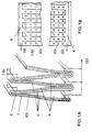
- Fig. 1a presents an embodiment of the invention, showing a densely folded (folds L) dielectric film element consisting of two film layers 1,2 placed one upon the other.
- the electric field is alternately strengthened and weakened in successive folds L by means of a control voltage.
- the film which is charged to charge Q, is coated in the successive folds with electrode layers K such that control electrodes of opposite sign are placed on opposite sides of the fold L.
- Such a film element can be manufactured e.g. from a permanently charged electret film or a three-layer film in which the middle layer consists of semiconducting material and is connected to a d.c.
- FIG. 1b illustrates the structure of the control electrodes K. Both consist of a rectangular edge and vertical bars starting from it and placed between the bars of the opposite electrode. Each fold L is joined at its ends with an adjacent fold L but is apart from adjacent folds at its middle portion. Such an element can be controlled using traditional amplifier equipment in sound reproduction applications.
- Sound reproduction devices employing the electrostatic principle generally use preforated stator plates and a thin movable electrode film between them. Since the force of the electric field affects the stator plates as well, undesirable resonances are generated in them. Moreover, the elements have to be large to produce a sufficient power.
- the sound reproduction device presented in this invention consists of only one folded film structure with electrodes formed on it.
- the electrodes K are arranged by connecting to the sides of the folds L in successive order a positive potential, a positive control signal ⁇ , a negative potential and a control signal - ⁇ in opposite phase.
- the electrodes K are connected by joining the same kind of electrodes together at the edge of the film.
- the voltage to the positive and negative electrodes can be connected via large resistances.
- the positive and negative charges can also be replaced with a so-called electret charge, which is injected into the dielectric film in a cyclic fashion with positive and negative charges alternating.
- the film of the invention can also be used for the measurement of sound or vibration, i.e. electric energy corresponding to the movement of the electrodes is induced in the ⁇ and - ⁇ electrodes.
- the film element shown in Fig. 1a can be manufactured from a thin plastic film with a metal plating on either side, in which the electrodes K are etched by using a technique employed in the manufacture of circuit boards. After this, the film is bent into folds L of a height of e.g. 1 - 10 mm with a distance of 0.1 mm between them.
- the structure presented in Fig. 2a consisting of two films, electret charges are placed between the films.
- the bars K of the electrodes are spaced at larger intervals and the positive and negative potentials are placed between them (Fig. 2b and 2c).
- this film element can be used as an active damping element when the control signal is set to zero.
- the element can be coated with protective layers 4, both of which may be e.g. thin films or one may be a thicker plate. It is possible to place several or at least two elements as shown in Fig. 3a on top of each other with protective layers 4 on the outermost surfaces.
- the voltage to the positive and negative electrodes is connected via a large resistance R1.
- Fig. 3c corresponds to Fig. 2b.
- the elements of the invention are very light and durable and have a large power capacity.
- the films 1,2 are preferably produced from plastic films containing flat gas bubbles because it has been established that such films retain their electret charge well and are as light as possible.
- a film of this type is presented in US patent specification 4654546.
- the invention is especially advantageous because the film movement is transverse to the sound direction, which means that the mass inertial forces of the film do not produce a counter moment in the direction of the sound.
- the elements function in a multi-effect manner. The air flowing between the folds L causes a viscose damping, and so does the visco-elastic motion of the films.
- the elements may also have a curved shape (Fig. 4b).
- the invention can also be utilized in many other applications designed to convert electric energy into mechanical motion or vibration, or conversely to convert mechanical motion or vibration into electric energy. In both cases, a very high efficiency is achieved.
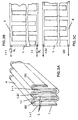
- Fig. 5 presents an application of the invention in which battens 7 are attached to each side of a wall 8 or plate and elements 5 and 6 are placed on the battens, the elements being electrically connected by conductors 9. A noise generates a change of charge in element 5. This is fed in opposite phase into element 6. If the wall has a passive damping of e.g. 20 dB and the elements have an efficiency of 10%, complete damping in both directions is achieved (Fig. 5b).
- the efficiency and damping of the elements can be adjusted by varying the + and - voltages or by selecting a suitable electret potential so as to obtain an optimal efficiency and the best damping for each practical application. Also, the folding density can be varied.
- a larger number of elements 5,6 can be used in an application, and the elements can be interconnected in various ways depending on the use.
- An active amplifier or filter circuit can also be used. Since the elements 5, 6 have a passive sound damping effect as well and may have a very high efficiency, it is not always necessary to use an intermediate passive damping layer.
- Fig. 6 presents an embodiment of the invention in which every third fold L is connected to the output of a controlling amplifier A whereas every second fold is sound-producing and connected as a feedback signal to the amplifier A.
- Fig. 7 presents a corresponding circuit implemented using electret films. The charges are on the surface of the folds L, and the opposite sides are provided with porous protective plates 10.
- Fig. 8 shows a structure in which an electret film (folds L) with a continuous metal plating 11 on one side acts as an element both producing and measuring sound.
Landscapes
- Physics & Mathematics (AREA)
- Engineering & Computer Science (AREA)
- Acoustics & Sound (AREA)
- Signal Processing (AREA)
- Electrostatic, Electromagnetic, Magneto- Strictive, And Variable-Resistance Transducers (AREA)
- Ceramic Capacitors (AREA)
- Surface Acoustic Wave Elements And Circuit Networks Thereof (AREA)
- Fixed Capacitors And Capacitor Manufacturing Machines (AREA)
- Piezo-Electric Transducers For Audible Bands (AREA)
- Basic Packing Technique (AREA)
- Treatment Of Fiber Materials (AREA)
- Yarns And Mechanical Finishing Of Yarns Or Ropes (AREA)
- Glass Compositions (AREA)
- Organic Low-Molecular-Weight Compounds And Preparation Thereof (AREA)
- Devices For Indicating Variable Information By Combining Individual Elements (AREA)
Applications Claiming Priority (3)
| Application Number | Priority Date | Filing Date | Title |
|---|---|---|---|
| FI932860 | 1993-06-21 | ||
| FI932860A FI104611B (fi) | 1993-06-21 | 1993-06-21 | Laskostettu energiamuunnin |
| PCT/FI1994/000278 WO1995001079A1 (en) | 1993-06-21 | 1994-06-21 | Folded dielectric film element and method for manufacturing the same |
Publications (2)
| Publication Number | Publication Date |
|---|---|
| EP0705527A1 EP0705527A1 (en) | 1996-04-10 |
| EP0705527B1 true EP0705527B1 (en) | 2000-04-19 |
Family
ID=8538177
Family Applications (1)
| Application Number | Title | Priority Date | Filing Date |
|---|---|---|---|
| EP94919686A Expired - Lifetime EP0705527B1 (en) | 1993-06-21 | 1994-06-21 | Folded dielectric film element and method for manufacturing the same |
Country Status (9)
| Country | Link |
|---|---|
| US (1) | US5757090A (da) |
| EP (1) | EP0705527B1 (da) |
| JP (1) | JP3532207B2 (da) |
| AT (1) | ATE192011T1 (da) |
| DE (1) | DE69424048T2 (da) |
| DK (1) | DK0705527T3 (da) |
| ES (1) | ES2145828T3 (da) |
| FI (1) | FI104611B (da) |
| WO (1) | WO1995001079A1 (da) |
Families Citing this family (12)
| Publication number | Priority date | Publication date | Assignee | Title |
|---|---|---|---|---|
| DE19802535C2 (de) * | 1998-01-23 | 2000-07-13 | Juergen Hesselbach | Mikroaktor |
| FI108986B (fi) | 1999-07-01 | 2002-04-30 | Emfitech Oy | Menetelmä anturielementin valmistamiseksi ja anturielementti |
| FI116605B (fi) * | 1999-11-05 | 2005-12-30 | Panphonics Oy | Akustinen elementti |
| FI108204B (fi) * | 1999-11-25 | 2001-11-30 | Kari Johannes Kirjavainen | Kalvo energioiden muuntamiseksi |
| US6873863B2 (en) * | 2001-03-19 | 2005-03-29 | Nokia Mobile Phones Ltd. | Touch sensitive navigation surfaces for mobile telecommunication systems |
| US7195840B2 (en) * | 2001-07-13 | 2007-03-27 | Kaun Thomas D | Cell structure for electrochemical devices and method of making same |
| US8021775B2 (en) * | 2001-07-13 | 2011-09-20 | Inventek Corporation | Cell structure for electrochemical devices and method of making same |
| US8734983B2 (en) * | 2004-04-14 | 2014-05-27 | Inventek Corporation | Housing for electrochemical devices |
| US7683467B2 (en) * | 2006-12-07 | 2010-03-23 | Stats Chippac Ltd. | Integrated circuit package system employing structural support |
| US9281763B2 (en) * | 2011-09-28 | 2016-03-08 | DigitalOptics Corporation MEMS | Row and column actuator control |
| JP6464317B2 (ja) * | 2015-09-02 | 2019-02-06 | コーニンクレッカ フィリップス エヌ ヴェKoninklijke Philips N.V. | 電気活性または光活性ポリマーをベースにしたアクチュエータデバイス |
| WO2018020887A1 (ja) * | 2016-07-27 | 2018-02-01 | 富士フイルム株式会社 | ピックアップセンサおよび生体センサ |
Family Cites Families (11)
| Publication number | Priority date | Publication date | Assignee | Title |
|---|---|---|---|---|
| GB212576A (da) * | 1923-03-08 | 1925-06-04 | Hermann Meusser | |
| US2855467A (en) * | 1953-12-11 | 1958-10-07 | Curry Electronics Inc | Loud speakers |
| US3008013A (en) * | 1954-07-20 | 1961-11-07 | Ferranti Ltd | Electrostatic loudspeakers |
| US3996922A (en) * | 1973-08-17 | 1976-12-14 | Electronic Monitors, Inc. | Flexible force responsive transducer |
| DE2900611A1 (de) * | 1979-01-09 | 1980-07-17 | Stefan Reich | Elektroakustischer wandler |
| FR2472901A1 (fr) * | 1979-12-28 | 1981-07-03 | Thomson Csf | Transducteur bimorphe en materiau polymere |
| US4725994A (en) * | 1984-06-14 | 1988-02-16 | Kabushiki Kaisha Toshiba | Ultrasonic transducer with a multiple-folded piezoelectric polymer film |
| US4654546A (en) * | 1984-11-20 | 1987-03-31 | Kari Kirjavainen | Electromechanical film and procedure for manufacturing same |
| US5219673A (en) * | 1991-08-23 | 1993-06-15 | Kaun Thomas D | Cell structure for electrochemical devices and method of making same |
| US5395592A (en) * | 1993-10-04 | 1995-03-07 | Bolleman; Brent | Acoustic liquid processing device |
| JP5218576B2 (ja) | 2011-02-03 | 2013-06-26 | 株式会社デンソー | 非接触給電制御装置及び非接触給電システム |
-
1993
- 1993-06-21 FI FI932860A patent/FI104611B/fi not_active IP Right Cessation
-
1994
- 1994-06-21 JP JP50248095A patent/JP3532207B2/ja not_active Expired - Fee Related
- 1994-06-21 DK DK94919686T patent/DK0705527T3/da active
- 1994-06-21 US US08/564,035 patent/US5757090A/en not_active Expired - Lifetime
- 1994-06-21 EP EP94919686A patent/EP0705527B1/en not_active Expired - Lifetime
- 1994-06-21 DE DE69424048T patent/DE69424048T2/de not_active Expired - Lifetime
- 1994-06-21 AT AT94919686T patent/ATE192011T1/de not_active IP Right Cessation
- 1994-06-21 WO PCT/FI1994/000278 patent/WO1995001079A1/en not_active Ceased
- 1994-06-21 ES ES94919686T patent/ES2145828T3/es not_active Expired - Lifetime
Also Published As
| Publication number | Publication date |
|---|---|
| DE69424048D1 (de) | 2000-05-25 |
| DK0705527T3 (da) | 2000-07-31 |
| DE69424048T2 (de) | 2000-09-14 |
| ATE192011T1 (de) | 2000-05-15 |
| ES2145828T3 (es) | 2000-07-16 |
| FI932860A0 (fi) | 1993-06-21 |
| FI104611B (fi) | 2000-02-29 |
| FI932860A7 (fi) | 1994-12-22 |
| US5757090A (en) | 1998-05-26 |
| EP0705527A1 (en) | 1996-04-10 |
| JP3532207B2 (ja) | 2004-05-31 |
| WO1995001079A1 (en) | 1995-01-05 |
| JPH08511671A (ja) | 1996-12-03 |
Similar Documents
| Publication | Publication Date | Title |
|---|---|---|
| EP0705527B1 (en) | Folded dielectric film element and method for manufacturing the same | |
| CA1071750A (en) | Transducer having piezoelectric film arranged with alternating curvatures | |
| US3544733A (en) | Electrostatic acoustic transducer | |
| US4028566A (en) | Electroacoustic conversion device having a diaphragm comprising at least one of a piezoelectric polymer material | |
| CN1997243B (zh) | 可挠式扬声器及其制法 | |
| US8391520B2 (en) | Flat speaker unit and speaker device therewith | |
| US3792204A (en) | Acoustic transducer using a piezoelectric polyvinylidene fluoride resin film as the oscillator | |
| JP5343053B2 (ja) | 電気機械変換器およびエネルギーを変換する方法 | |
| US3894198A (en) | Electrostatic-piezoelectric transducer | |
| JP5512834B2 (ja) | 電気活性ポリマーの予歪み | |
| EP1042822A4 (en) | PIEZOELECTRIC TRANSDUCER | |
| GB1597615A (en) | Electro-acoustic device | |
| US10804818B2 (en) | Triboelectric generator and network for mechanical energy harvesting | |
| CA2430741A1 (en) | Electrostatic device | |
| CN113543001B (zh) | 电容式传感器、麦克风以及电子设备 | |
| Kim et al. | Improvement of low-frequency characteristics of piezoelectric speakers based on acoustic diaphragms | |
| JP4138004B2 (ja) | 音響部材と音響処理方法 | |
| CN110021287A (zh) | 一种声学超材料 | |
| FI115598B (fi) | Akustinen elementti | |
| WO2022110349A1 (zh) | 一种压电式麦克风及其制作方法 | |
| JPH0513118Y2 (da) | ||
| US8526654B2 (en) | Acoustic wave generation device and equipment including a plurality of such devices | |
| CN220545119U (zh) | 振动传感器及车载扬声器系统 | |
| JPS61155700A (ja) | 圧電バイモルフ振動板を用いた送風機 | |
| RU2071186C1 (ru) | Электроакустический преобразователь |
Legal Events
| Date | Code | Title | Description |
|---|---|---|---|
| PUAI | Public reference made under article 153(3) epc to a published international application that has entered the european phase |
Free format text: ORIGINAL CODE: 0009012 |
|
| 17P | Request for examination filed |
Effective date: 19960108 |
|
| AK | Designated contracting states |
Kind code of ref document: A1 Designated state(s): AT BE CH DE DK ES FR GB IT LI NL SE |
|
| RAP1 | Party data changed (applicant data changed or rights of an application transferred) |
Owner name: PANPHONICS OY |
|
| RIN1 | Information on inventor provided before grant (corrected) |
Inventor name: KIRJAVAINEN, KARI |
|
| GRAG | Despatch of communication of intention to grant |
Free format text: ORIGINAL CODE: EPIDOS AGRA |
|
| 17Q | First examination report despatched |
Effective date: 19990622 |
|
| GRAG | Despatch of communication of intention to grant |
Free format text: ORIGINAL CODE: EPIDOS AGRA |
|
| GRAH | Despatch of communication of intention to grant a patent |
Free format text: ORIGINAL CODE: EPIDOS IGRA |
|
| GRAH | Despatch of communication of intention to grant a patent |
Free format text: ORIGINAL CODE: EPIDOS IGRA |
|
| GRAA | (expected) grant |
Free format text: ORIGINAL CODE: 0009210 |
|
| AK | Designated contracting states |
Kind code of ref document: B1 Designated state(s): AT BE CH DE DK ES FR GB IT LI NL SE |
|
| REF | Corresponds to: |
Ref document number: 192011 Country of ref document: AT Date of ref document: 20000515 Kind code of ref document: T |
|
| REG | Reference to a national code |
Ref country code: CH Ref legal event code: EP |
|
| REG | Reference to a national code |
Ref country code: CH Ref legal event code: NV Representative=s name: KIRKER & CIE SA |
|
| REF | Corresponds to: |
Ref document number: 69424048 Country of ref document: DE Date of ref document: 20000525 |
|
| ITF | It: translation for a ep patent filed | ||
| ET | Fr: translation filed | ||
| REG | Reference to a national code |
Ref country code: ES Ref legal event code: FG2A Ref document number: 2145828 Country of ref document: ES Kind code of ref document: T3 |
|
| REG | Reference to a national code |
Ref country code: DK Ref legal event code: T3 |
|
| PLBE | No opposition filed within time limit |
Free format text: ORIGINAL CODE: 0009261 |
|
| STAA | Information on the status of an ep patent application or granted ep patent |
Free format text: STATUS: NO OPPOSITION FILED WITHIN TIME LIMIT |
|
| 26N | No opposition filed | ||
| REG | Reference to a national code |
Ref country code: GB Ref legal event code: IF02 |
|
| PGFP | Annual fee paid to national office [announced via postgrant information from national office to epo] |
Ref country code: NL Payment date: 20040530 Year of fee payment: 11 |
|
| PGFP | Annual fee paid to national office [announced via postgrant information from national office to epo] |
Ref country code: CH Payment date: 20040602 Year of fee payment: 11 |
|
| PGFP | Annual fee paid to national office [announced via postgrant information from national office to epo] |
Ref country code: SE Payment date: 20040603 Year of fee payment: 11 Ref country code: AT Payment date: 20040603 Year of fee payment: 11 |
|
| PGFP | Annual fee paid to national office [announced via postgrant information from national office to epo] |
Ref country code: DK Payment date: 20040604 Year of fee payment: 11 |
|
| PGFP | Annual fee paid to national office [announced via postgrant information from national office to epo] |
Ref country code: ES Payment date: 20040615 Year of fee payment: 11 |
|
| PGFP | Annual fee paid to national office [announced via postgrant information from national office to epo] |
Ref country code: BE Payment date: 20040709 Year of fee payment: 11 |
|
| PG25 | Lapsed in a contracting state [announced via postgrant information from national office to epo] |
Ref country code: IT Free format text: LAPSE BECAUSE OF NON-PAYMENT OF DUE FEES;WARNING: LAPSES OF ITALIAN PATENTS WITH EFFECTIVE DATE BEFORE 2007 MAY HAVE OCCURRED AT ANY TIME BEFORE 2007. THE CORRECT EFFECTIVE DATE MAY BE DIFFERENT FROM THE ONE RECORDED. Effective date: 20050621 Ref country code: AT Free format text: LAPSE BECAUSE OF NON-PAYMENT OF DUE FEES Effective date: 20050621 |
|
| PG25 | Lapsed in a contracting state [announced via postgrant information from national office to epo] |
Ref country code: SE Free format text: LAPSE BECAUSE OF NON-PAYMENT OF DUE FEES Effective date: 20050622 Ref country code: ES Free format text: LAPSE BECAUSE OF NON-PAYMENT OF DUE FEES Effective date: 20050622 |
|
| PG25 | Lapsed in a contracting state [announced via postgrant information from national office to epo] |
Ref country code: LI Free format text: LAPSE BECAUSE OF NON-PAYMENT OF DUE FEES Effective date: 20050630 Ref country code: DK Free format text: LAPSE BECAUSE OF NON-PAYMENT OF DUE FEES Effective date: 20050630 Ref country code: CH Free format text: LAPSE BECAUSE OF NON-PAYMENT OF DUE FEES Effective date: 20050630 Ref country code: BE Free format text: LAPSE BECAUSE OF NON-PAYMENT OF DUE FEES Effective date: 20050630 |
|
| PG25 | Lapsed in a contracting state [announced via postgrant information from national office to epo] |
Ref country code: NL Free format text: LAPSE BECAUSE OF NON-PAYMENT OF DUE FEES Effective date: 20060101 |
|
| REG | Reference to a national code |
Ref country code: CH Ref legal event code: PL |
|
| EUG | Se: european patent has lapsed | ||
| NLV4 | Nl: lapsed or anulled due to non-payment of the annual fee |
Effective date: 20060101 |
|
| REG | Reference to a national code |
Ref country code: DK Ref legal event code: EBP |
|
| REG | Reference to a national code |
Ref country code: ES Ref legal event code: FD2A Effective date: 20050622 |
|
| BERE | Be: lapsed |
Owner name: *PANPHONICS OY Effective date: 20050630 |
|
| PGFP | Annual fee paid to national office [announced via postgrant information from national office to epo] |
Ref country code: DE Payment date: 20130620 Year of fee payment: 20 Ref country code: GB Payment date: 20130619 Year of fee payment: 20 |
|
| PGFP | Annual fee paid to national office [announced via postgrant information from national office to epo] |
Ref country code: FR Payment date: 20130703 Year of fee payment: 20 |
|
| REG | Reference to a national code |
Ref country code: DE Ref legal event code: R071 Ref document number: 69424048 Country of ref document: DE |
|
| REG | Reference to a national code |
Ref country code: GB Ref legal event code: PE20 Expiry date: 20140620 |
|
| PG25 | Lapsed in a contracting state [announced via postgrant information from national office to epo] |
Ref country code: GB Free format text: LAPSE BECAUSE OF EXPIRATION OF PROTECTION Effective date: 20140620 |
|
| PG25 | Lapsed in a contracting state [announced via postgrant information from national office to epo] |
Ref country code: DE Free format text: LAPSE BECAUSE OF EXPIRATION OF PROTECTION Effective date: 20140624 |