EP0704838A1 - Verfahren zur Herstellung einer strukturierten magnetischen Speicherplatte - Google Patents
Verfahren zur Herstellung einer strukturierten magnetischen Speicherplatte Download PDFInfo
- Publication number
- EP0704838A1 EP0704838A1 EP95306771A EP95306771A EP0704838A1 EP 0704838 A1 EP0704838 A1 EP 0704838A1 EP 95306771 A EP95306771 A EP 95306771A EP 95306771 A EP95306771 A EP 95306771A EP 0704838 A1 EP0704838 A1 EP 0704838A1
- Authority
- EP
- European Patent Office
- Prior art keywords
- substrate
- film
- texture
- layer
- magnetic
- Prior art date
- Legal status (The legal status is an assumption and is not a legal conclusion. Google has not performed a legal analysis and makes no representation as to the accuracy of the status listed.)
- Withdrawn
Links
Images


Classifications
-
- G—PHYSICS
- G11—INFORMATION STORAGE
- G11B—INFORMATION STORAGE BASED ON RELATIVE MOVEMENT BETWEEN RECORD CARRIER AND TRANSDUCER
- G11B5/00—Recording by magnetisation or demagnetisation of a record carrier; Reproducing by magnetic means; Record carriers therefor
- G11B5/84—Processes or apparatus specially adapted for manufacturing record carriers
- G11B5/8404—Processes or apparatus specially adapted for manufacturing record carriers manufacturing base layers
-
- G—PHYSICS
- G11—INFORMATION STORAGE
- G11B—INFORMATION STORAGE BASED ON RELATIVE MOVEMENT BETWEEN RECORD CARRIER AND TRANSDUCER
- G11B5/00—Recording by magnetisation or demagnetisation of a record carrier; Reproducing by magnetic means; Record carriers therefor
- G11B5/62—Record carriers characterised by the selection of the material
- G11B5/73—Base layers, i.e. all non-magnetic layers lying under a lowermost magnetic recording layer, e.g. including any non-magnetic layer in between a first magnetic recording layer and either an underlying substrate or a soft magnetic underlayer
- G11B5/7368—Non-polymeric layer under the lowermost magnetic recording layer
- G11B5/7369—Two or more non-magnetic underlayers, e.g. seed layers or barrier layers
- G11B5/737—Physical structure of underlayer, e.g. texture
-
- G—PHYSICS
- G11—INFORMATION STORAGE
- G11B—INFORMATION STORAGE BASED ON RELATIVE MOVEMENT BETWEEN RECORD CARRIER AND TRANSDUCER
- G11B5/00—Recording by magnetisation or demagnetisation of a record carrier; Reproducing by magnetic means; Record carriers therefor
- G11B5/62—Record carriers characterised by the selection of the material
- G11B5/73—Base layers, i.e. all non-magnetic layers lying under a lowermost magnetic recording layer, e.g. including any non-magnetic layer in between a first magnetic recording layer and either an underlying substrate or a soft magnetic underlayer
- G11B5/739—Magnetic recording media substrates
- G11B5/73911—Inorganic substrates
- G11B5/73917—Metallic substrates, i.e. elemental metal or metal alloy substrates
-
- G—PHYSICS
- G11—INFORMATION STORAGE
- G11B—INFORMATION STORAGE BASED ON RELATIVE MOVEMENT BETWEEN RECORD CARRIER AND TRANSDUCER
- G11B5/00—Recording by magnetisation or demagnetisation of a record carrier; Reproducing by magnetic means; Record carriers therefor
- G11B5/62—Record carriers characterised by the selection of the material
- G11B5/73—Base layers, i.e. all non-magnetic layers lying under a lowermost magnetic recording layer, e.g. including any non-magnetic layer in between a first magnetic recording layer and either an underlying substrate or a soft magnetic underlayer
- G11B5/739—Magnetic recording media substrates
- G11B5/73911—Inorganic substrates
- G11B5/73921—Glass or ceramic substrates
-
- G—PHYSICS
- G11—INFORMATION STORAGE
- G11B—INFORMATION STORAGE BASED ON RELATIVE MOVEMENT BETWEEN RECORD CARRIER AND TRANSDUCER
- G11B5/00—Recording by magnetisation or demagnetisation of a record carrier; Reproducing by magnetic means; Record carriers therefor
- G11B5/62—Record carriers characterised by the selection of the material
- G11B5/73—Base layers, i.e. all non-magnetic layers lying under a lowermost magnetic recording layer, e.g. including any non-magnetic layer in between a first magnetic recording layer and either an underlying substrate or a soft magnetic underlayer
- G11B5/739—Magnetic recording media substrates
- G11B5/73923—Organic polymer substrates
Definitions
- This invention relates to a thin film magnetic disk recording medium. More particularly the invention relates to texturing a recording medium.
- magnetic thin film disks comprise a substrate on which a non-magnetic underlayer, a magnetic layer and a protective overcoat are deposited by vacuum deposition, followed by application of a thin layer of lubricant.
- a non-magnetic underlayer a magnetic layer and a protective overcoat are deposited by vacuum deposition, followed by application of a thin layer of lubricant.
- An example of such a disk is described in U.S. Patent 5,180,640, incorporated herein by reference. It is known to use, as a substrate, ceramic material, glass, or an aluminum alloy coated with electrochemically deposited nickel-phosphorus ("NiP").
- the disk is rotated rapidly by a motor.
- a recording head "flies" very close to the rotating disk.
- the recording head typically rests in contact with the disk when the disk is not rotating.
- the surface of the disk is intentionally roughened or "textured".
- texturing is usually done by abrading the electrochemically deposited NiP surface with fine particles to form circumferential ridges. Other texturing methods are also known in the art.
- texturing may be done by chemically etching the substrate to leave bumps, or covering the surface with fine particles.
- U.S. Patent 4,833,001 discloses a typical etching process.
- the recording head flies as close to the disk surface as possible.
- the abrasive texturing method cannot be used for typical non-metallic disk substrates because of their hardness, so other methods such as chemical or plasma etching or coating the substrate with a fine dispersion of particles, have been adopted.
- these processes like abrasive texturing, are expensive in production as they require a number of process steps to be applied to each substrate.
- any irregularities that protrude sufficiently above the normal textured surface can damage the head while the head is flying and can cause the head to crash.
- each texturing method is specific to a particular substrate material so that changing the composition or type of the substrate material requires the development of a new texturing method.
- a method for forming a magnetic disk comprising the steps of:
- the invention also provides a magnetic disk comprising:
- Advantageous embodiments of the present invention are directed to reducing stiction by introducing surface roughness to an initially smooth substrate by depositing one or more sputtered films which grow with a controlled roughness determined by the sputter conditions and materials selected.
- the roughness is introduced by growing a continuous, low melting point material film (a "texture film”).
- This texture film develops a surface roughness as its grains grow.
- Ra values are as measured by an atomic force microscope).
- the rate of change of roughness with film thickness correlates approximately inversely with the melting point (more properly, the self-diffusion coefficient) of the material selected.
- Zn films roughen more quickly with film thickness than Al films
- Al films roughen more quickly than Cu films.
- the roughness also depends on the sputter mode (r.f. sputtered films roughen more easily than d.c. sputtered films) and on the sputtering conditions (e.g., roughening is enhanced by higher pressures and higher substrate temperatures).
- the texture film is continuous, i.e. it covers the substrate without leaving pores or gaps.
- the density of asperities, i.e. the roughness peaks also depends on the choice of materials and deposition parameters.
- a low-melting point material e.g. a metal such as Al, Zn, Sn, Pb, their alloys or other low melting point metals or alloys
- r.f. sputtering an elevated substrate temperature (but not high enough to warp or damage the substrate) and a high sputter pressure (e.g. 20 to 30 mTorr).
- This gives a texture film with the requisite roughness (Ra about 2 to about 5 nm) for a relatively thin sputtered film (e.g. 20 to 60 nm thick).
- a thin film is desirable in order to reduce process time and material usage.
- low melting point materials used to form the texture film are often mechanically soft and if the film is thin there is less possibility of damaging or deforming it.
- a more refractory sputtered texture film such as Cu, Cu-Zn, Ag, Au, or other metals, alloys or ceramics
- the costs of a thicker film to obtain the same Ra is offset by the improved film hardness.
- the texture film is continuous.
- the texture film can prevent impurities such as oxygen from migrating from the substrate surface upward to where they could have a detrimental effect on the magnetic layer.
- the condition of the substrate surface prior to sputtering should be less critical then it is in other disk manufacturing processes.
- an adhesion layer may be sputtered between the texture film and the underlying substrate to enhance adhesion.
- Materials used in this adhesion layer typically include Cr, Ta, Ti, W, Nb, V, Zr, Mo or their alloys. This optional adhesion layer need not contribute to the surface roughness.
- a capping layer may be sputtered over the texture film to protect the texture film from mechanical damage caused by impact of the recording head against the magnetic disk during use.
- Suitable materials include hard layers such as Cr, Ta, Ti, W, Mo, Nb, Zr, V, alloys thereof, or hard ceramic materials such as SiO2, Al2O3, ZrB2, TiC or other hard oxides, carbides or nitrides.
- the capping layer does not significantly affect surface roughness but it does provide a hard overcoat to protect the texture film from damage. (The adhesion layer also helps protect the disk against mechanical damage.)
- the magnetic stack (an underlayer, magnetic layer and overcoat layer) is then sputtered on top of the capping layer (or if there is no capping layer, on top of the texture film).
- the texture method of the invention allows formation of a texture of controlled roughness on an initially smooth substrate with the surface texture characteristics controlled via the sputter deposition parameters and choice of materials.
- This method is a more economical method of making a controlled surface texture since the rough sputtered texture film and the optional adhesion and capping layers can be deposited in the same pass-by sputter system as the other sputtered layers on the disk. This eliminates the need for separate texturing processes.
- the texture film may also be deposited in a separate sputter system, but is still economical due to the high throughput of the sputter system.
- Texturing can be applied to a smooth or polished substrate made of a range of materials, including metallic substrates, glass, ceramics, sintered carbon, canasite or glass-ceramics.
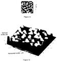
- Figs. 1 to 4 are enlarged schematic cross-section views of a magnetic disk textured in accordance with four embodiments of my invention.
- Fig. 5 illustrates the relationship between roughness of disks made with a 40 nm thick texture film and the melting point of the texture film material.
- Fig. 6 is a scanning electron microscope ("SEM") photograph showing the morphology of a 45 nm thick Al film sputtered onto a glass substrate.
- Fig. 7 is a SEM photograph of a 55 nm thick Zn film sputtered onto a glass substrate.
- Fig. 8 is a SEM photograph of a 220 nm thick Cu film sputtered onto a glass substrate.
- Fig. 9 is a SEM photograph of a 12 nm thick 90% Cu/10% Zn alloy film sputtered onto a glass substrate.
- Fig. 10 is an atomic force microscope ("AFM") micrograph of a 3 ⁇ m x 3 ⁇ m section of the top surface of a disk comprising a smooth glass substrate having a 21 nm thick Al texture film sputtered thereon, and covered by sputtered NiP, a magnetic Co-Ni-Cr-Pt alloy and a carbon protective overcoat.
- AFM atomic force microscope
- Fig. 11 is a perspective AFM micrograph of the structure of Fig. 10.
- Fig. 12 is an AFM micrograph of the top surface of a disk comprising a smooth glass substrate having a 45 nm thick Al texture film sputtered thereon, and covered by sputtered NiP, a magnetic Co-Ni-Cr-Pt alloy and a carbon protective overcoat.
- Fig. 13 is a perspective AFM micrograph of the structure of Fig. 12.
- Fig. 14 is an AFM micrograph of the top surface of a disk comprising a smooth glass substrate having an 110 nm thick Al texture film sputtered thereon, and covered by sputtered NiP, a magnetic Co-Ni-Cr-Pt alloy, and a carbon protective overcoat.
- Fig. 15 is a perspective AFM micrograph of the structure of Fig. 14.
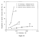
- Fig. 16 shows the relationship between the thickness of an Al texture film and the film roughness for Al sputtered onto a glass substrate, Al sputtered onto a 25 nm thick Ti layer formed on a glass substrate and Al sputtered onto a 25 nm thick Cr layer formed on a glass substrate.
- Fig. 17 shows the relationship of the thickness of Al texture films and resultant roughness Ra of disks comprising the Al texture films sputtered at 20°C and 250°C onto smooth glass, and for a disk comprising an Al texture film sputtered at 20°C and covered by a Cr capping layer.
- Fig. 18 shows the relationship between roughness and thickness for Al sputtered directly onto a smooth glass substrate by r.f. and d.c. magnetron sputtering.
- Fig. 19 shows the relationship between roughness and sputtering pressure for a 200 nm thick Al film d.c. magnetron sputtered at a power density of 50 W/cm.
- Figs. 20 to 22 and 24 to 27 illustrate the results of contact-start-stop (“CSS”) tests for disks including Al texture films of various thicknesses.
- Fig. 23 and 27 illustrate the results of a CSS test for a conventional circumferentially textured magnetic disk.
- Fig. 28 is a graph of a glide signal vs. disk radius in inches for a disk comprising a polished substrate covered with plated NiP, covered by sputtered 25 nm thick Cr, 66 nm thick Al, a NiP underlayer, a Co-Ni-Cr-Pt magnetic alloy and carbon.
- Fig. 29 is a graph of a glide signal vs. disk radius for a conventional circumferentially textured disk.
- a magnetic disk 10 includes a substrate 11 made of sodium borosilicate, sodalime or other glass, an aluminum alloy coated with NiP and then polished, other metals, ceramics or sintered carbon.
- Substrate 11 is typically smooth, and generally has a roughness Ra less than about 2 nm, and on average may be about 1 nm.
- the invention may be used with a very smooth substrate, e.g. having an Ra of 0.2 nm or less.
- Substrate 11 is coated with an adhesion layer 12 to promote improved adhesion with subsequently deposited layers.
- Adhesion layer 12 is preferably a coating of a refractory metal or a transition metal from one of the earlier columns of the periodic table, such as Cr, Ta, Ti, Mo, V, W, Nb, Sc, Y or Zr, or alloys thereof, applied by r.f. magnetron, r.f. diode, d.c. magnetron or d.c. diode sputtering.
- a refractory metal or a transition metal from one of the earlier columns of the periodic table such as Cr, Ta, Ti, Mo, V, W, Nb, Sc, Y or Zr, or alloys thereof, applied by r.f. magnetron, r.f. diode, d.c. magnetron or d.c. diode sputtering.
- sputtering may be at 20 mtorr of pressure in an argon atmosphere and a power density of 2 W/cm.
- pressure may be at 10 mtorr in
- the subsequently deposited texture film 14 typically forms a stronger bond to a freshly sputtered adhesion layer (e.g. Cr) than it would to as received substrate 11 because there is a better chance of forming a strong chemical bond between layer 12 and film 14, e.g. a strong intermetallic bond for the case in which both layer 12 and film 14 are metals.
- a freshly sputtered adhesion layer e.g. Cr
- adhesion layer 12 is not critical as long as layer 12 can improve the adhesion of subsequently formed layers to substrate 11. A 2 to 50 nm thickness may be used, but a 2 to 20 nm thickness is preferred since it is easier and more economical to form a thinner adhesion layer. While adhesion layer 12 may be useful, other embodiments of my invention (e.g. as shown in Figs. 3 and 4) do not include layer 12.
- a low melting metal e.g. a melting point less than about 1000°C and preferably less than 750°C
- a low melting point such as Al, Zn, Pb, Sn, Bi, In, Li or Se, or alloys thereof
- substrate 11 and optional layer 12 are at a temperature between 20 and 200°C.
- a planar r.f. magnetron sputtering machine with an argon gas pressure of from about 10 to about 30 mtorr and a power density of from about 1 to about 6 W/cm is preferably utilized to sputter film 14.
- the sputtering machine may be a model PE 4400 machine available from Perkin Elmer Co. of Minnesota. However, in other embodiments of the invention, other sputtering systems, pressures, and power densities are used.
- the low melting point metal film 14 develops a rough microtexture on its top surface as it grows. Development of grains or crystals on the surface of the growing layer produces the surface texture. Film 14 is the primary means of microtexturing the substrate over the entire substrate surface, upon which a magnetic alloy layer is to be subsequently deposited.
- the peak density and height of the asperities or roughness Ra are controlled by the sputtering operating parameters. It has been found that an Ra from about 2 to 10 nm and a peak pitch of from about 0.1 to 1 ⁇ m gives satisfactory results.
- Ra of 2 to 5 nm is preferred, depending on the head used with the disk.
- European patent application 0 583 989 A2 discusses selecting head and disk roughness characteristics.
- Typical peak densities are between about 1 to 100 per ⁇ m.
- a hard capping layer 15 of Cr, Ta, Ti or any suitably hard material may be sputtered by the same sputtering machine a similar pressure and power density.
- Capping layer 15 is typically 10 to 100 nm thick, and preferably 10 to 30 nm thick.
- the sputtering conditions by which layer 15 is formed are not critical. In general, capping layer 15 does not enhance disk roughness, but it can be made to enhance roughness, e.g. depending on thickness and sputtering conditions such as substrate temperature as described below. While capping layer 15 may be useful, other embodiments of my invention (e.g. as shown in Figs. 2 and 4) do not include layer 15.
- an underlayer 16 such as NiP, a magnetic layer 17 (typically a Co alloy) and an overcoat 18 (typically carbon) are then deposited by additional sputtering operations.
- Carbon layer 18 is then suitably lubricated in the conventional manner using a perfluoropolyether or other lubricant.
- NiP sputtered underlayers in magnetic disks are described in U.S. patent 5,153,044, incorporated herein by reference.
- NiP layer 16 serves as a nucleation layer for magnetic layer 17, and is typically formed because it has a beneficial effect on the magnetic alloy. However, in other embodiments, layer 16 need not be formed.
- underlayers comprising materials other than NiP (particularly Cr and Cr alloys) can be used.
- Carbon as a protective overcoat on a magnetic disk is described in European patent application 0 440 259 A2, also incorporated herein by reference.
- Protective materials other than carbon such as ZrO2 can also be used as a protective overcoat on a magnetic disk in accordance with my invention. See, for example, U.S. Patents 4,929,500 and 4,898,774, incorporated herein by reference.
- the higher the melting point for a material the greater the thickness one must use to achieve a given roughness. It is desirable to be able to achieve a roughness Ra between 2 to 5 nm with a texture film thickness less than about 60 nm. Accordingly, it may be desirable to use a material having a melting point less than about 1000°C to form film 14. However, it may also be desirable to use a material having a higher melting point to form film 14, e.g., because such materials tend to have greater mechanical strength. For example, a metal such as Cu, Ag, Au, an alloy such as Cu-Zn, or a ceramic material can be used in texture film 14. However, if a higher melting point material is used, that material must be a) sputtered to a greater thickness, and/or b) sputtered at a higher substrate temperature to achieve a desired roughness.
- a thin rough texture film can also be achieved with a more refractory material (e.g. transition metals from the later columns of the periodic table such as Cu, Ag, Au or an alloy such as Cu-Zn) at an elevated substrate temperature (e.g. about 200°C) and a greater thickness (e.g. 100 to 200 nm) using r.f. sputtering at a high pressure.
- a more refractory material e.g. transition metals from the later columns of the periodic table such as Cu, Ag, Au or an alloy such as Cu-Zn
- a greater thickness e.g. 100 to 200 nm
- Fig. 5 shows the roughness of a disk with a 25 nm thick Cr adhesion layer and a texture film having a thickness of 40 nm graphed against the melting point of the material used to form the texture film.
- Sn, Zn, Al, Ag, a 90% Cu-10% Zn alloy, and Cu were used to form the texture films in Fig. 5.
- roughness correlates clossely to melting point.
- the texture films in Fig. 5 were all sputtered at 20 mtorr of argon and a power density of 1.5 W/cm by r.f. sputtering.
- texture film roughness increases with thickness.
- Figs. 6 to 9 are SEM micrographs at a 100K magnification showing respectively the growth in 2 minutes, 30 seconds, 4 minutes and 2 minutes a 45 nm thick of Al layer, a 55 nm thick Zn layer, a 220 nm thick Cu layer and a 120 nm thick 90% Cu-10% Zn layer.
- Each were sputtered using the above identified Perkin Elmer sputtering apparatus at a pressure of 20 mtorr of Ar using a power density of 0.5 W/cm with an 8" (20.3 cm) target on a 95 mm thick glass substrate.
- These figures show that the roughness of the asperities (crystals) which provide the rough surface texture grow at different rates.
- thin Al is rougher and has a larger grain size than thicker CuZn sputtered under comparable conditions.
- grain size and roughness increase with film thickness.
- the disks included sputtered NiP, Co-Ni-Cr-Pt and carbon layers formed thereon. The height and pitch of the asperities are shown in the respective perspective micrographs.
- the thicker the texture film the larger the growths that are formed, and the rougher the disk texture.
- Figure 16 illustrates roughness versus thickness for an Al film formed directly on a smooth glass substrate (curve 20), Al formed on a 25 nm thick Ti adhesion layer which in turn is formed on a glass substrate (curve 22), and Al formed on a 25 nm thick Cr adhesion layer formed on a glass substrate (curve 24).
- Curve 20 Al formed on a 25 nm thick Ti adhesion layer which in turn is formed on a glass substrate
- Curve 24 Al formed on a 25 nm thick Cr adhesion layer formed on a glass substrate
- Fig. 17 illustrates the relation between the roughness of disks including sputtered Al texture films and the Al texture film thickness for films sputtered at room temperature (20°C) and 250°C (curves 25 and 28, respectively).
- the substrate In order to ensure Ra values of from about 2 to 5 nm with a film thickness less than 60 nm, the substrate should preferably be in a temperature range of 20°C to 200°C.
- Satisfactory Ra values can be achieved with an Al film thickness in the range from about 20 to 60 nm.
- the bottom curve 26 shows that an added Cr capping layer (layer 15 in Fig. 1) of 25 nm does not affect resultant roughness.
- Upper curve 28 shows that roughness increases much more rapidly as a function of thickness at high substrate temperatures.
- One way to form such an Al film is to sputter using a substrate temperature of 20°C to a thickness of 45 nm.
- Another way is to sputter a 15 nm thick Al film using a substrate temperature of 250°C.
- the drawback of using higher substrate temperatures includes possible warping of Al/NiP substrates above 250°C, but this is not a problem for other typical substrate materials.
- one of ordinary skill in the art will be able, in light of this disclosure, to select the temperature and thickness combination that is most convenient.
- the operating points shift (e.g. one needs a higher substrate temperature and/or greater thickness to achieve a Ra of 5 nm), but the same principles apply (e.g. a higher temperature yields a steeper roughness vs. thickness curve).
- Fig. 18 shows the relation between roughness and thickness for Al sputtered directly on a smooth glass substrate by r.f. and d.c. magnetron sputtering.
- r.f. magnetron sputtering produces a much rougher film (curve 36) than d.c. magnetron sputtering (curve 38) for a given film thickness and the same sputter system.
- Curve 40 shows the relationship between roughness and thickness for films d.c. magnetron-sputtered in a different sputter system (model SCD-12Z11, manufactured by Ulvac Corp. of Japan), at lower pressure and higher power. Table I lists the conditions under which the films of curves 36, 38, and 40 were formed.
- Curves 36, 38, and 40 were generated using room temperature substrates. Since the roughness achieved under the conditions of curve 40 is less than that of curves 36 and 38, it may be necessary to form a thick film and/or use a higher substrate temperature to achieve a particular desired roughness. However, as seen in Fig. 26 (discussed below), a desired roughness can be achieved using the curve 40 system at the indicated pressure and power density.
- the invention can be used in an in-line sputter system using r.f. sputtering with pressures of about 10 to 30 mtorr and relatively low power densities (about 1 to 6 W/cm), similar to the apparatus described in the '259 European patent application, in which the adhesion layer 12, texture film 14, capping layer 15 and the magnetic stack are deposited in one pass. Texture film 14 can also be deposited economically in a separate high throughput machine (e.g. about 500 disks/hour) such as the Ulvac system described above. Other sputtering systems are also suitable for use in my invention.
- Fig. 19 shows the relationship between roughness and pressure for a 200 nm thick Al film d.c. magnetron-sputtered at a relatively high power (50 W/cm) and low pressure to achieve high throughput.
- roughness increases as pressure increases.
- Roughness also increases with temperature.
- the texture film must be made thick and/or sputtered using an elevated substrate temperature to get a desired roughness.
- island formation was observed at elevated substrate temperatures (250°C and over) with very thin films (e.g. about 10 nm).
- the present invention achieves demonstrably satisfactory textures at lower substrate temperatures (e.g. 20°C and above) with films less than about 60 nm thick, depending on metal material selection of film 14 (Fig. 1) and sputter conditions.
- Figs. 20, 21 and 22 indicate the result of CSS (stiction) testing of complete disks textured in accordance with my invention showing better performance than a conventional circumferentially textured disk of the prior art (Fig. 23).
- the prior art disk had an Ra of about 7 nm.
- the CSS tests in Figs. 20 to 23 were accomplished using a 70% recording head while a 7 gram force was applied to the head against the disk. (The term "70%" in this context is a well-known term in the industry, and refers to the head size. A 70% head is 2.3 x 3.3 mm.) During the Fig. 20 to 23 tests, the disk was rotated to 3600 rpm and then stopped 15000 times. The stiction force between the head and disk was measured.
- Table II below describes the disks used in Figs. 20 to 27.
- Figs. 24 to 27 were done under the same conditions as those of Figs. 20 to 23, except using a 3 gram loading force and a 50% slider. (Again, the term “50% slider” refers to a slider having the following dimensions: 1.7x2.4 mm).
- the test of Figs. 24 to 27 were much less rigorous than those of Figs. 20 to 23. It is seen that in each case, stiction was below 4 grams.
- the disk of Fig. 26 (Al thickness equal 200 nm) exhibited behavior superior to the prior art disk of Fig. 27.
- the disks of Figs. 25 and 27 exhibited comparable performance. This comparable performance was achieved without the extra abrasion steps needed to build the disk of Fig. 27.
- Fig. 22 shows that the method of the present invention works on substrates comprising an aluminum alloy coated with NiP as well as glass substrates.
- Fig. 28 shows that the sputter textured disk of the invention can support a 1.5 ⁇ " (38 nm) glide height.
- the glide height is a measure of disk roughness.
- a read-write head flies at a fixed low height over the magnetic disk.
- a piezo-electric transducer affixed to the head suspension generates a voltage proportional to the strength of the interaction between the head and disk. In most cases, the voltage is roughly proportional to the height of the asperity.
- Fig. 28 shows the maximum piezo-electric transducer contact voltage for each disk track vs. radius (distance between the center of the disk and the track). In other words, Fig. 28 provides a measure of the highest asperity on each track. If the output voltage exceeds that corresponding to a test criterion (e.g. a 2 ⁇ " (51 nm) asperity), the disk is considered a glide test reject.
- the disk used to generate Fig. 28 included a polished substrate comprising an aluminum alloy disk coated with NiP, a 25 nm Cr adhesion layer, a 66 nm Al texture film, an NiP underlayer, a CoNiCrPt magnetic alloy and a carbon overcoat. (All layers deposited on the aluminum alloy disk except the first NiP coating were sputtered.)
- Fig. 28 The few voltage spikes appearing in Fig. 28 were probably due to contamination or dust particles. Upon retesting, the voltage spikes showed up in different locations. A horizontal line in Fig. 28 corresponds to the voltage a 1.5 ⁇ " high asperity would produce. As can be seen, other than the few voltage spikes which are believed to be caused by sources other than asperities, the disk of Fig. 28 passes a 1.5 ⁇ " glide height test with ease.
- Fig. 29 shows the result of a glide test on a conventional disk. As can be seen, the glide signal of Fig. 29 indicates that there were many asperities on the conventional disk compared to the disk of Fig. 28.
- the present invention is typically practiced using an initially smooth substrate, e.g. having an Ra between about 0.2 and 2 nm.
- initial substrate roughnesses less than 0.2 nm can also be used.
- Disks in accordance with my invention can be produced using vacuum deposition techniques other than sputtering, e.g. chemical vapor deposition or evaporation.
- vacuum deposition techniques other than sputtering, e.g. chemical vapor deposition or evaporation.
- the same general principles, such as the relation between material melting point, thickness and roughness as described above apply to other vacuum deposition techniques.
Landscapes
- Chemical & Material Sciences (AREA)
- Engineering & Computer Science (AREA)
- Inorganic Chemistry (AREA)
- Ceramic Engineering (AREA)
- Manufacturing & Machinery (AREA)
- Metallurgy (AREA)
- Magnetic Record Carriers (AREA)
- Manufacturing Of Magnetic Record Carriers (AREA)
Applications Claiming Priority (2)
| Application Number | Priority Date | Filing Date | Title |
|---|---|---|---|
| US08/313,704 US5871621A (en) | 1994-09-27 | 1994-09-27 | Method of fabricating a textured magnetic storage disk |
| US313704 | 1994-09-27 |
Publications (1)
| Publication Number | Publication Date |
|---|---|
| EP0704838A1 true EP0704838A1 (de) | 1996-04-03 |
Family
ID=23216787
Family Applications (1)
| Application Number | Title | Priority Date | Filing Date |
|---|---|---|---|
| EP95306771A Withdrawn EP0704838A1 (de) | 1994-09-27 | 1995-09-26 | Verfahren zur Herstellung einer strukturierten magnetischen Speicherplatte |
Country Status (3)
| Country | Link |
|---|---|
| US (1) | US5871621A (de) |
| EP (1) | EP0704838A1 (de) |
| JP (1) | JPH08180407A (de) |
Cited By (1)
| Publication number | Priority date | Publication date | Assignee | Title |
|---|---|---|---|---|
| GB2338336B (en) * | 1997-01-15 | 2000-11-29 | Seagate Technology | Magnetic recording medium |
Families Citing this family (14)
| Publication number | Priority date | Publication date | Assignee | Title |
|---|---|---|---|---|
| KR100318175B1 (ko) * | 1995-10-18 | 2002-02-19 | 가나이 쓰도무 | 자기디스크및자기기록재생장치 |
| JP3371062B2 (ja) * | 1996-11-05 | 2003-01-27 | 株式会社日立製作所 | 磁気記録媒体、その製造方法及び磁気記憶装置 |
| JPH11339240A (ja) * | 1998-05-27 | 1999-12-10 | Fujitsu Ltd | 磁気記録媒体及び磁気ディスク装置 |
| US6316097B1 (en) | 1998-09-28 | 2001-11-13 | Seagate Technology Llc | Electroless plating process for alternative memory disk substrates |
| US6545974B1 (en) | 1998-11-18 | 2003-04-08 | Seagate Technology Llc | Disc media and methods for fabricating |
| US6611400B1 (en) * | 1999-01-22 | 2003-08-26 | Seagate Technology Llc | Texture structure for optimizing head disc interface |
| US6830600B2 (en) | 2000-04-14 | 2004-12-14 | Seagate Technology Llc | Cold traps for vapor lubrication processes |
| JP2003059034A (ja) * | 2001-08-23 | 2003-02-28 | Fujitsu Ltd | 磁気記録媒体用ガラス基板及び磁気記録媒体 |
| US20050074635A1 (en) * | 2002-03-19 | 2005-04-07 | Nippon Sheet Glass Co., Ltd. | Information recording medium and method of manufacturing glass substrate for the information recording medium, and glass substrate for the information recording medium, manufactured using the method |
| US6787251B1 (en) | 2002-04-19 | 2004-09-07 | Seagate Technology Llc | Recording medium with a varying composition underlayer |
| US20050070097A1 (en) * | 2003-09-29 | 2005-03-31 | International Business Machines Corporation | Atomic laminates for diffusion barrier applications |
| WO2006011611A1 (en) * | 2004-07-30 | 2006-02-02 | Showa Denko K.K. | Method of producing a magnetic recording medium |
| JP2006147130A (ja) * | 2004-10-21 | 2006-06-08 | Showa Denko Kk | 垂直磁気記録媒体の製造方法及び垂直磁気記録媒体 |
| KR20080073395A (ko) * | 2007-02-06 | 2008-08-11 | 삼성전자주식회사 | 수직 자기 기록 방식의 자기 기록 매체 및 그를 구비한하드디스크 드라이브 |
Citations (9)
| Publication number | Priority date | Publication date | Assignee | Title |
|---|---|---|---|---|
| US4833001A (en) | 1986-10-09 | 1989-05-23 | Asahi Glass Company Ltd. | Glass substrate for a magnetic disc and process for its production |
| US4898774A (en) | 1986-04-03 | 1990-02-06 | Komag, Inc. | Corrosion and wear resistant magnetic disk |
| US4929500A (en) | 1986-04-03 | 1990-05-29 | Komag, Inc. | Corrosion resistant magnetic disk |
| EP0421120A2 (de) * | 1989-10-05 | 1991-04-10 | International Business Machines Corporation | Magnetischer Dünnfilmspeicher und Verfahren zu seiner Herstellung |
| US5153044A (en) | 1987-02-25 | 1992-10-06 | Komag, Inc. | Magnetic disk for longitudinal recording comprising an amorphous intermediate layer |
| US5180640A (en) | 1990-10-01 | 1993-01-19 | Komag, Inc. | Magnetic recording medium comprising a magnetic alloy layer of cobalt nickel, platinum and chromium formed directly on a nickel alloy amorphous underlayer |
| EP0534624A1 (de) * | 1991-09-24 | 1993-03-31 | International Business Machines Corporation | Magnetische Aufzeichnungsplatte |
| WO1994015720A1 (en) * | 1993-01-07 | 1994-07-21 | Akashic Memories Corporation | Magnetic recording media on non-metallic substrates and methods for their production |
| DE4341306A1 (de) * | 1993-01-20 | 1994-07-21 | Fuji Electric Co Ltd | Magnetisches Aufzeichnungsmedium und Verfahren zu seiner Herstellung |
Family Cites Families (6)
| Publication number | Priority date | Publication date | Assignee | Title |
|---|---|---|---|---|
| GB2167448B (en) * | 1984-11-02 | 1988-10-19 | Hitachi Ltd | Perpendicular magnetic recording medium |
| JPS62256215A (ja) * | 1986-04-28 | 1987-11-07 | Hoya Corp | 磁気記録媒体 |
| JPS63237210A (ja) * | 1987-03-25 | 1988-10-03 | Sony Corp | 磁気記録媒体 |
| JP2728498B2 (ja) * | 1988-05-27 | 1998-03-18 | 株式会社日立製作所 | 磁気記録媒体 |
| US5132173A (en) * | 1989-02-10 | 1992-07-21 | Canon Kabushiki Kaisha | Magnetic recording medium having a silicon oxide protective layer with an electrical specific resistance of from 3.3×10¹³ to 5.0×15 ohm.cm |
| ES2074538T3 (es) * | 1989-05-22 | 1995-09-16 | Nippon Sheet Glass Co Ltd | Sustrato utilizado para un disco magnetico y medio de gabracion magnetico que utiliza el sustrato. |
-
1994
- 1994-09-27 US US08/313,704 patent/US5871621A/en not_active Expired - Fee Related
-
1995
- 1995-09-26 EP EP95306771A patent/EP0704838A1/de not_active Withdrawn
- 1995-09-26 JP JP7247352A patent/JPH08180407A/ja active Pending
Patent Citations (9)
| Publication number | Priority date | Publication date | Assignee | Title |
|---|---|---|---|---|
| US4898774A (en) | 1986-04-03 | 1990-02-06 | Komag, Inc. | Corrosion and wear resistant magnetic disk |
| US4929500A (en) | 1986-04-03 | 1990-05-29 | Komag, Inc. | Corrosion resistant magnetic disk |
| US4833001A (en) | 1986-10-09 | 1989-05-23 | Asahi Glass Company Ltd. | Glass substrate for a magnetic disc and process for its production |
| US5153044A (en) | 1987-02-25 | 1992-10-06 | Komag, Inc. | Magnetic disk for longitudinal recording comprising an amorphous intermediate layer |
| EP0421120A2 (de) * | 1989-10-05 | 1991-04-10 | International Business Machines Corporation | Magnetischer Dünnfilmspeicher und Verfahren zu seiner Herstellung |
| US5180640A (en) | 1990-10-01 | 1993-01-19 | Komag, Inc. | Magnetic recording medium comprising a magnetic alloy layer of cobalt nickel, platinum and chromium formed directly on a nickel alloy amorphous underlayer |
| EP0534624A1 (de) * | 1991-09-24 | 1993-03-31 | International Business Machines Corporation | Magnetische Aufzeichnungsplatte |
| WO1994015720A1 (en) * | 1993-01-07 | 1994-07-21 | Akashic Memories Corporation | Magnetic recording media on non-metallic substrates and methods for their production |
| DE4341306A1 (de) * | 1993-01-20 | 1994-07-21 | Fuji Electric Co Ltd | Magnetisches Aufzeichnungsmedium und Verfahren zu seiner Herstellung |
Cited By (1)
| Publication number | Priority date | Publication date | Assignee | Title |
|---|---|---|---|---|
| GB2338336B (en) * | 1997-01-15 | 2000-11-29 | Seagate Technology | Magnetic recording medium |
Also Published As
| Publication number | Publication date |
|---|---|
| JPH08180407A (ja) | 1996-07-12 |
| US5871621A (en) | 1999-02-16 |
Similar Documents
| Publication | Publication Date | Title |
|---|---|---|
| US4610911A (en) | Thin film magnetic recording media | |
| US5580667A (en) | Multilayered medium with gradient isolation layer | |
| US6277506B1 (en) | Thin film magnetic head thin film magnetic head substrate and method for fabricating such substrate | |
| EP0704838A1 (de) | Verfahren zur Herstellung einer strukturierten magnetischen Speicherplatte | |
| US5569506A (en) | Magnetic recording disk and disk drive with improved head-disk interface | |
| US5820969A (en) | Magnetic recording medium | |
| EP0421120B1 (de) | Magnetischer Dünnfilmspeicher und Verfahren zu seiner Herstellung | |
| JP3018762B2 (ja) | 磁気記録媒体およびその製造方法 | |
| US5705287A (en) | Magnetic recording disk with metal nitride texturing layer | |
| EP0840293B1 (de) | Magnetisches Aufzeichnungsmedium, Herstellungsverfahren für dasselbe und magnetischer Speicher | |
| US4631202A (en) | Thin film magnetic recording film | |
| US6524730B1 (en) | NiFe-containing soft magnetic layer design for multilayer media | |
| US5506017A (en) | Method for texturing magnetic media | |
| US5413835A (en) | Magnetic recording medium having an underlayer of low melting point metal alloy in the form of spherically shaped structures | |
| EP0534624B1 (de) | Magnetische Aufzeichnungsplatte | |
| EP0381652A2 (de) | Carbonüberzug für eine magnetische Dünnfilmaufzeichnungsplatte | |
| US6878439B2 (en) | Magnetic recording medium, its production process and magnetic recording device | |
| US5399386A (en) | In-situ texturing of a thin film magnetic medium | |
| US6846543B2 (en) | Thin film magnetic recording disk with ruthenium-aluminum layer | |
| US20030049497A1 (en) | Oriented magnetic medium on a nonmetallic substrate | |
| KR100629034B1 (ko) | 패턴화된 기판을 가진 자기 기록 매체 | |
| JP3682132B2 (ja) | 磁気記録媒体の製造方法 | |
| JPH10283626A (ja) | 磁気記録媒体及びその製造方法 | |
| JP2853529B2 (ja) | 磁気記録媒体用基板およびそれを用いた磁気記録媒体 | |
| JPH08227520A (ja) | 磁気記録媒体及びその製造方法 |
Legal Events
| Date | Code | Title | Description |
|---|---|---|---|
| PUAI | Public reference made under article 153(3) epc to a published international application that has entered the european phase |
Free format text: ORIGINAL CODE: 0009012 |
|
| AK | Designated contracting states |
Kind code of ref document: A1 Designated state(s): DE GB NL |
|
| 17P | Request for examination filed |
Effective date: 19961001 |
|
| 17Q | First examination report despatched |
Effective date: 19970523 |
|
| STAA | Information on the status of an ep patent application or granted ep patent |
Free format text: STATUS: THE APPLICATION IS DEEMED TO BE WITHDRAWN |
|
| 18D | Application deemed to be withdrawn |
Effective date: 20001031 |