EP0704732A1 - Integrierter optoelektronischer Verbund und Stecker - Google Patents
Integrierter optoelektronischer Verbund und Stecker Download PDFInfo
- Publication number
- EP0704732A1 EP0704732A1 EP95306828A EP95306828A EP0704732A1 EP 0704732 A1 EP0704732 A1 EP 0704732A1 EP 95306828 A EP95306828 A EP 95306828A EP 95306828 A EP95306828 A EP 95306828A EP 0704732 A1 EP0704732 A1 EP 0704732A1
- Authority
- EP
- European Patent Office
- Prior art keywords
- base
- substrate
- submount
- array
- channels
- Prior art date
- Legal status (The legal status is an assumption and is not a legal conclusion. Google has not performed a legal analysis and makes no representation as to the accuracy of the status listed.)
- Granted
Links
Images


Classifications
-
- G—PHYSICS
- G02—OPTICS
- G02B—OPTICAL ELEMENTS, SYSTEMS OR APPARATUS
- G02B6/00—Light guides; Structural details of arrangements comprising light guides and other optical elements, e.g. couplings
- G02B6/24—Coupling light guides
- G02B6/42—Coupling light guides with opto-electronic elements
- G02B6/4201—Packages, e.g. shape, construction, internal or external details
- G02B6/4204—Packages, e.g. shape, construction, internal or external details the coupling comprising intermediate optical elements, e.g. lenses, holograms
- G02B6/421—Packages, e.g. shape, construction, internal or external details the coupling comprising intermediate optical elements, e.g. lenses, holograms the intermediate optical component consisting of a short length of fibre, e.g. fibre stub
-
- G—PHYSICS
- G02—OPTICS
- G02B—OPTICAL ELEMENTS, SYSTEMS OR APPARATUS
- G02B6/00—Light guides; Structural details of arrangements comprising light guides and other optical elements, e.g. couplings
- G02B6/24—Coupling light guides
- G02B6/42—Coupling light guides with opto-electronic elements
- G02B6/4201—Packages, e.g. shape, construction, internal or external details
- G02B6/4249—Packages, e.g. shape, construction, internal or external details comprising arrays of active devices and fibres
-
- G—PHYSICS
- G02—OPTICS
- G02B—OPTICAL ELEMENTS, SYSTEMS OR APPARATUS
- G02B6/00—Light guides; Structural details of arrangements comprising light guides and other optical elements, e.g. couplings
- G02B6/24—Coupling light guides
- G02B6/42—Coupling light guides with opto-electronic elements
- G02B6/4201—Packages, e.g. shape, construction, internal or external details
- G02B6/4219—Mechanical fixtures for holding or positioning the elements relative to each other in the couplings; Alignment methods for the elements, e.g. measuring or observing methods especially used therefor
- G02B6/4228—Passive alignment, i.e. without a detection of the degree of coupling or the position of the elements
- G02B6/423—Passive alignment, i.e. without a detection of the degree of coupling or the position of the elements using guiding surfaces for the alignment
- G02B6/4231—Passive alignment, i.e. without a detection of the degree of coupling or the position of the elements using guiding surfaces for the alignment with intermediate elements, e.g. rods and balls, between the elements
-
- G—PHYSICS
- G02—OPTICS
- G02B—OPTICAL ELEMENTS, SYSTEMS OR APPARATUS
- G02B6/00—Light guides; Structural details of arrangements comprising light guides and other optical elements, e.g. couplings
- G02B6/24—Coupling light guides
- G02B6/42—Coupling light guides with opto-electronic elements
- G02B6/4201—Packages, e.g. shape, construction, internal or external details
- G02B6/4219—Mechanical fixtures for holding or positioning the elements relative to each other in the couplings; Alignment methods for the elements, e.g. measuring or observing methods especially used therefor
- G02B6/4228—Passive alignment, i.e. without a detection of the degree of coupling or the position of the elements
- G02B6/4232—Passive alignment, i.e. without a detection of the degree of coupling or the position of the elements using the surface tension of fluid solder to align the elements, e.g. solder bump techniques
-
- G—PHYSICS
- G02—OPTICS
- G02B—OPTICAL ELEMENTS, SYSTEMS OR APPARATUS
- G02B6/00—Light guides; Structural details of arrangements comprising light guides and other optical elements, e.g. couplings
- G02B6/24—Coupling light guides
- G02B6/42—Coupling light guides with opto-electronic elements
- G02B6/4201—Packages, e.g. shape, construction, internal or external details
- G02B6/4219—Mechanical fixtures for holding or positioning the elements relative to each other in the couplings; Alignment methods for the elements, e.g. measuring or observing methods especially used therefor
- G02B6/4236—Fixing or mounting methods of the aligned elements
- G02B6/4238—Soldering
-
- G—PHYSICS
- G02—OPTICS
- G02B—OPTICAL ELEMENTS, SYSTEMS OR APPARATUS
- G02B6/00—Light guides; Structural details of arrangements comprising light guides and other optical elements, e.g. couplings
- G02B6/24—Coupling light guides
- G02B6/42—Coupling light guides with opto-electronic elements
- G02B6/4292—Coupling light guides with opto-electronic elements the light guide being disconnectable from the opto-electronic element, e.g. mutually self aligning arrangements
-
- H—ELECTRICITY
- H01—ELECTRIC ELEMENTS
- H01L—SEMICONDUCTOR DEVICES NOT COVERED BY CLASS H10
- H01L2224/00—Indexing scheme for arrangements for connecting or disconnecting semiconductor or solid-state bodies and methods related thereto as covered by H01L24/00
- H01L2224/01—Means for bonding being attached to, or being formed on, the surface to be connected, e.g. chip-to-package, die-attach, "first-level" interconnects; Manufacturing methods related thereto
- H01L2224/42—Wire connectors; Manufacturing methods related thereto
- H01L2224/47—Structure, shape, material or disposition of the wire connectors after the connecting process
- H01L2224/48—Structure, shape, material or disposition of the wire connectors after the connecting process of an individual wire connector
- H01L2224/4805—Shape
- H01L2224/4809—Loop shape
- H01L2224/48091—Arched
-
- H—ELECTRICITY
- H01—ELECTRIC ELEMENTS
- H01L—SEMICONDUCTOR DEVICES NOT COVERED BY CLASS H10
- H01L2224/00—Indexing scheme for arrangements for connecting or disconnecting semiconductor or solid-state bodies and methods related thereto as covered by H01L24/00
- H01L2224/01—Means for bonding being attached to, or being formed on, the surface to be connected, e.g. chip-to-package, die-attach, "first-level" interconnects; Manufacturing methods related thereto
- H01L2224/42—Wire connectors; Manufacturing methods related thereto
- H01L2224/47—Structure, shape, material or disposition of the wire connectors after the connecting process
- H01L2224/48—Structure, shape, material or disposition of the wire connectors after the connecting process of an individual wire connector
- H01L2224/484—Connecting portions
- H01L2224/48463—Connecting portions the connecting portion on the bonding area of the semiconductor or solid-state body being a ball bond
- H01L2224/48465—Connecting portions the connecting portion on the bonding area of the semiconductor or solid-state body being a ball bond the other connecting portion not on the bonding area being a wedge bond, i.e. ball-to-wedge, regular stitch
-
- H—ELECTRICITY
- H01—ELECTRIC ELEMENTS
- H01L—SEMICONDUCTOR DEVICES NOT COVERED BY CLASS H10
- H01L2924/00—Indexing scheme for arrangements or methods for connecting or disconnecting semiconductor or solid-state bodies as covered by H01L24/00
- H01L2924/30—Technical effects
- H01L2924/301—Electrical effects
- H01L2924/3025—Electromagnetic shielding
Definitions
- the invention also provides a hermetically sealed optoelectronic package comprising:
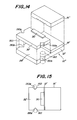
- the submount 32 with the laser diode array 30 premounted to it, is then assembled to the base 12.
- the submount 32 is placed on the base surface 28 between the guide pins 64.
- the width of the submount between its opposite surfaces 56, 58 is precisely matched, during its manufacture, to the spacing between the guide pins 64.
- the submount 32 therefore fits precisely between the two pins 64 on the base surface 28, thereby positioning the laser diodes of the array 30 in optical alignment with the end faces 68 of the optical fibers 40.
- the assembled scrambler unit 100 can be aligned with the triangular channels containing the optical fibers by inserting guide segments of optical fiber or rigid pins of the same diameter as the fibers through the triangular channels 106 of the scrambler unit and into the triangular channels of the optical fiber holder, i.e. between the upper substrate 16 and lower substrate 18.
- the scrambler unit 102 can also be aligned by means of the same guide pins 64, shown in Figures 6 through 8, passing through pin guide passages of the scrambler unit analogous to the pin guides 26 of the upper substrate 16 in Figures 1 and 2.
- the upper substrate 102 of scrambler unit can be a slice taken from a V-grooved substrate 16, including the pin guide portions of that substrate.
Priority Applications (1)
| Application Number | Priority Date | Filing Date | Title |
|---|---|---|---|
| EP01110737A EP1143278B1 (de) | 1994-09-28 | 1995-09-27 | Integrierter optoelektronischer Verbund und Stecker |
Applications Claiming Priority (2)
| Application Number | Priority Date | Filing Date | Title |
|---|---|---|---|
| US08/313,765 US5535296A (en) | 1994-09-28 | 1994-09-28 | Integrated optoelectronic coupling and connector |
| US313765 | 1994-09-28 |
Related Child Applications (1)
| Application Number | Title | Priority Date | Filing Date |
|---|---|---|---|
| EP01110737A Division EP1143278B1 (de) | 1994-09-28 | 1995-09-27 | Integrierter optoelektronischer Verbund und Stecker |
Publications (2)
| Publication Number | Publication Date |
|---|---|
| EP0704732A1 true EP0704732A1 (de) | 1996-04-03 |
| EP0704732B1 EP0704732B1 (de) | 2002-03-06 |
Family
ID=23217055
Family Applications (2)
| Application Number | Title | Priority Date | Filing Date |
|---|---|---|---|
| EP95306828A Expired - Lifetime EP0704732B1 (de) | 1994-09-28 | 1995-09-27 | Integrierter optoelektronischer Verbund und Stecker |
| EP01110737A Expired - Lifetime EP1143278B1 (de) | 1994-09-28 | 1995-09-27 | Integrierter optoelektronischer Verbund und Stecker |
Family Applications After (1)
| Application Number | Title | Priority Date | Filing Date |
|---|---|---|---|
| EP01110737A Expired - Lifetime EP1143278B1 (de) | 1994-09-28 | 1995-09-27 | Integrierter optoelektronischer Verbund und Stecker |
Country Status (4)
| Country | Link |
|---|---|
| US (2) | US5535296A (de) |
| EP (2) | EP0704732B1 (de) |
| JP (2) | JP3143051B2 (de) |
| DE (2) | DE69535291T2 (de) |
Cited By (12)
| Publication number | Priority date | Publication date | Assignee | Title |
|---|---|---|---|---|
| EP0826886A1 (de) * | 1996-08-29 | 1998-03-04 | Kabushiki Kaisha Toshiba | Optisches Einkristallmodul |
| EP0826996A1 (de) * | 1996-07-31 | 1998-03-04 | Kyocera Corporation | Halteteil für optische Elemente und Verfahren zu dessen Herstellung |
| WO2000021130A1 (en) * | 1998-10-08 | 2000-04-13 | Honeywell Inc. | Methods and apparatus for hermetically sealing electronic packages |
| EP1111420A2 (de) * | 1999-12-20 | 2001-06-27 | Talltec Sensors S.A. | Optische Verbindungsvorrichtung |
| EP1139130A1 (de) * | 2000-03-27 | 2001-10-04 | Ngk Insulators, Ltd. | Halterung für ein Array von optischen Fasern |
| EP1139134A2 (de) * | 2000-03-31 | 2001-10-04 | Ngk Insulators, Ltd. | Verbindung zwischen Lichtleitfaser und optischem Element |
| US7338218B2 (en) | 2005-02-01 | 2008-03-04 | Ibiden Co., Ltd. | Optical module, method of manufacturing the optical module, and data communication system including the optical module |
| US7438484B2 (en) | 2005-04-06 | 2008-10-21 | Ibiden Co., Ltd. | Electrical connector for a multi form-factor pluggable transceiver, and data communication system including the electrical connector |
| US7559703B2 (en) | 2005-09-14 | 2009-07-14 | Ibiden Co., Ltd. | Optical module and data communication system including the optical module |
| CN102736185A (zh) * | 2011-04-01 | 2012-10-17 | 鸿富锦精密工业(深圳)有限公司 | 光纤耦合连接器 |
| CN102955204A (zh) * | 2011-08-25 | 2013-03-06 | 鸿富锦精密工业(深圳)有限公司 | 光纤耦合连接器 |
| US20140126861A1 (en) * | 2012-11-08 | 2014-05-08 | Hon Hai Precision Industry Co., Ltd. | Fixing device for optical fiber detection |
Families Citing this family (99)
| Publication number | Priority date | Publication date | Assignee | Title |
|---|---|---|---|---|
| US5555333A (en) * | 1993-07-12 | 1996-09-10 | Ricoh Company, Ltd. | Optical module and a fabrication process thereof |
| JP3345518B2 (ja) * | 1994-09-28 | 2002-11-18 | 株式会社東芝 | 光半導体モジュールの製造方法 |
| US5546281A (en) | 1995-01-13 | 1996-08-13 | Methode Electronics, Inc. | Removable optoelectronic transceiver module with potting box |
| US6220878B1 (en) | 1995-10-04 | 2001-04-24 | Methode Electronics, Inc. | Optoelectronic module with grounding means |
| US5717533A (en) | 1995-01-13 | 1998-02-10 | Methode Electronics Inc. | Removable optoelectronic module |
| JPH09318849A (ja) * | 1996-05-24 | 1997-12-12 | Fujitsu Ltd | 光伝送モジュールおよびその製造方法 |
| US6840936B2 (en) * | 1996-10-22 | 2005-01-11 | Epicor Medical, Inc. | Methods and devices for ablation |
| DE19709842C1 (de) * | 1997-02-28 | 1998-10-15 | Siemens Ag | Elektrooptische Koppelbaugruppe |
| DE19711283A1 (de) * | 1997-03-18 | 1998-10-29 | Siemens Ag | Hermetisch dichtes optisches Sendemodul |
| US6215944B1 (en) | 1997-03-27 | 2001-04-10 | Ngk Insulators, Ltd. | Sealed fiber array and method for manufacturing a sealed fiber array |
| US5930428A (en) * | 1997-08-12 | 1999-07-27 | Rockwell Science Center, Inc. | Blind-mate fiber optic connector with integral optoelectronic receiver circuits |
| US6085007A (en) * | 1998-02-27 | 2000-07-04 | Jiang; Ching-Long | Passive alignment member for vertical surface emitting/detecting device |
| US6713788B2 (en) | 1998-03-30 | 2004-03-30 | Micron Technology, Inc. | Opto-electric mounting apparatus |
| US6380563B2 (en) | 1998-03-30 | 2002-04-30 | Micron Technology, Inc. | Opto-electric mounting apparatus |
| US6095697A (en) * | 1998-03-31 | 2000-08-01 | Honeywell International Inc. | Chip-to-interface alignment |
| US6049650A (en) * | 1998-04-17 | 2000-04-11 | Seagate Technology, Inc. | Structure for micro-machine optical tooling and method for making and using |
| US6473553B1 (en) | 1998-04-17 | 2002-10-29 | Seagate Technology Llc | Apparatus for holding and engaging micro-machined objects and method for making same |
| US6203333B1 (en) | 1998-04-22 | 2001-03-20 | Stratos Lightwave, Inc. | High speed interface converter module |
| US6179627B1 (en) | 1998-04-22 | 2001-01-30 | Stratos Lightwave, Inc. | High speed interface converter module |
| US6172997B1 (en) | 1998-06-16 | 2001-01-09 | Aculight Corporation | Integrated semiconductor diode laser pumped solid state laser |
| DE19843164C2 (de) * | 1998-09-21 | 2000-11-23 | Harting Elektrooptische Bauteile Gmbh & Co Kg | Steckerteil für eine optische Steckverbindung |
| US6292615B1 (en) | 1999-03-09 | 2001-09-18 | Uniphase Telecommunications Products, Inc. | Optical fiber feedthrough |
| US6445837B1 (en) | 1999-03-31 | 2002-09-03 | Nu-Wave Photonics, Inc. | Hybrid opto-electronic circuits and method of making |
| US6498880B1 (en) * | 1999-03-31 | 2002-12-24 | Picolight Incorporated | Fiber optic ferrule |
| US6873800B1 (en) | 1999-05-26 | 2005-03-29 | Jds Uniphase Corporation | Hot pluggable optical transceiver in a small form pluggable package |
| US7013088B1 (en) | 1999-05-26 | 2006-03-14 | Jds Uniphase Corporation | Method and apparatus for parallel optical interconnection of fiber optic transmitters, receivers and transceivers |
| US6213651B1 (en) | 1999-05-26 | 2001-04-10 | E20 Communications, Inc. | Method and apparatus for vertical board construction of fiber optic transmitters, receivers and transceivers |
| US6632030B2 (en) | 1999-05-27 | 2003-10-14 | E20 Communications, Inc. | Light bending optical block for fiber optic modules |
| US20020033979A1 (en) * | 1999-05-27 | 2002-03-21 | Edwin Dair | Method and apparatus for multiboard fiber optic modules and fiber optic module arrays |
| US20020030872A1 (en) * | 1999-05-27 | 2002-03-14 | Edwin Dair | Method and apparatus for multiboard fiber optic modules and fiber optic module arrays |
| US7116912B2 (en) * | 1999-05-27 | 2006-10-03 | Jds Uniphase Corporation | Method and apparatus for pluggable fiber optic modules |
| US20040069997A1 (en) * | 1999-05-27 | 2004-04-15 | Edwin Dair | Method and apparatus for multiboard fiber optic modules and fiber optic module arrays |
| US6952532B2 (en) * | 1999-05-27 | 2005-10-04 | Jds Uniphase Corporation | Method and apparatus for multiboard fiber optic modules and fiber optic module arrays |
| US20010048793A1 (en) * | 1999-05-27 | 2001-12-06 | Edwin Dair | Method and apparatus for multiboard fiber optic modules and fiber optic module arrays |
| US6220873B1 (en) | 1999-08-10 | 2001-04-24 | Stratos Lightwave, Inc. | Modified contact traces for interface converter |
| US6373644B1 (en) * | 1999-11-15 | 2002-04-16 | Axsun Technologies, Inc. | Micro optical bench component clip structures |
| US6583902B1 (en) | 1999-12-09 | 2003-06-24 | Alvesta, Inc. | Modular fiber-optic transceiver |
| EP1108677B1 (de) * | 1999-12-15 | 2006-09-27 | Asulab S.A. | Hermetische In-Situ-Gehäusungsmethode von Mikrosystemen |
| US6704515B1 (en) | 1999-12-30 | 2004-03-09 | The Boeing Company | Fiber optic interface module and associated fabrication method |
| US6866426B1 (en) | 2000-04-07 | 2005-03-15 | Shipley Company, L.L.C. | Open face optical fiber array for coupling to integrated optic waveguides and optoelectronic submounts |
| US6848839B2 (en) * | 2000-04-07 | 2005-02-01 | Shipley Company, L.L.C. | Methods and devices for coupling optoelectronic packages |
| US6916121B2 (en) | 2001-08-03 | 2005-07-12 | National Semiconductor Corporation | Optical sub-assembly for optoelectronic modules |
| SE519713C2 (sv) * | 2000-05-23 | 2003-04-01 | Ericsson Telefon Ab L M | Förfarande och anordning för passiv upplinjering |
| US6741778B1 (en) | 2000-05-23 | 2004-05-25 | International Business Machines Corporation | Optical device with chip level precision alignment |
| US6788853B2 (en) * | 2000-06-28 | 2004-09-07 | Shipley Company, L.L.C. | Method for cleaving integrated optic waveguides to provide a smooth waveguide endface |
| US6474879B1 (en) * | 2000-08-08 | 2002-11-05 | Stratos Lightwave, Inc. | Post assembly metallization of a device to form hermetic seal |
| US6464407B1 (en) | 2000-10-13 | 2002-10-15 | Berg Technology, Inc. | Optical connector having a ferrule with alignment and sealing features |
| US7021836B2 (en) * | 2000-12-26 | 2006-04-04 | Emcore Corporation | Attenuator and conditioner |
| US6799902B2 (en) * | 2000-12-26 | 2004-10-05 | Emcore Corporation | Optoelectronic mounting structure |
| US20020122637A1 (en) * | 2000-12-26 | 2002-09-05 | Anderson Gene R. | Optical transmitter, receiver or transceiver module |
| US6956999B2 (en) | 2001-02-20 | 2005-10-18 | Cyberoptics Corporation | Optical device |
| US6546172B2 (en) | 2001-02-20 | 2003-04-08 | Avanti Optics Corporation | Optical device |
| US6443631B1 (en) | 2001-02-20 | 2002-09-03 | Avanti Optics Corporation | Optical module with solder bond |
| US20040212802A1 (en) * | 2001-02-20 | 2004-10-28 | Case Steven K. | Optical device with alignment compensation |
| US6546173B2 (en) * | 2001-02-20 | 2003-04-08 | Avanti Optics Corporation | Optical module |
| US6635866B2 (en) | 2001-04-19 | 2003-10-21 | Internation Business Machines Corporation | Multi-functional fiber optic coupler |
| US7269027B2 (en) * | 2001-08-03 | 2007-09-11 | National Semiconductor Corporation | Ceramic optical sub-assembly for optoelectronic modules |
| US7023705B2 (en) * | 2001-08-03 | 2006-04-04 | National Semiconductor Corporation | Ceramic optical sub-assembly for optoelectronic modules |
| US6631228B2 (en) | 2001-09-14 | 2003-10-07 | Photon-X, Inc. | Adhesive-free bonding method of fiber attachment for polymer optical waveguide on polymer substrate |
| US7476906B2 (en) * | 2002-01-09 | 2009-01-13 | Osram Opto Semiconductors Gmbh | Photodiode array and method for establishing a link between a first semiconductor element and a second semiconductor element |
| US7123798B2 (en) * | 2002-03-29 | 2006-10-17 | Ngk Insulators, Ltd. | Optical device and method of producing the same |
| DE10233203B4 (de) * | 2002-07-22 | 2006-08-03 | Mergeoptics Gmbh | Modul mit einem Lichtleitelement und Verfahren zum Herstellen |
| US20040264870A1 (en) * | 2002-08-20 | 2004-12-30 | Skunes Timothy A. | Optical alignment mount with height adjustment |
| US7195402B2 (en) * | 2002-12-20 | 2007-03-27 | Ngk Insulators, Ltd. | Optical device |
| US7308174B2 (en) * | 2002-12-20 | 2007-12-11 | Ngk Insulators, Ltd. | Optical device including a filter member for dividing a portion of signal light |
| US7321703B2 (en) * | 2002-12-20 | 2008-01-22 | Ngk Insulators, Ltd. | Optical device |
| JP4031804B2 (ja) * | 2003-06-02 | 2008-01-09 | 日本碍子株式会社 | 光デバイス |
| US6883978B2 (en) * | 2003-06-26 | 2005-04-26 | Matsushita Electric Industrial Co., Ltd. | Low cost package design for fiber coupled optical component |
| US7284913B2 (en) | 2003-07-14 | 2007-10-23 | Matsushita Electric Industrial Co., Ltd. | Integrated fiber attach pad for optical package |
| US7156562B2 (en) * | 2003-07-15 | 2007-01-02 | National Semiconductor Corporation | Opto-electronic module form factor having adjustable optical plane height |
| US6942397B2 (en) * | 2003-07-25 | 2005-09-13 | Xponent Photonics Inc | Packaging for a fiber-coupled optical device |
| US7410088B2 (en) * | 2003-09-05 | 2008-08-12 | Matsushita Electric Industrial, Co., Ltd. | Solder preform for low heat stress laser solder attachment |
| US7021838B2 (en) | 2003-12-16 | 2006-04-04 | Matsushita Electric Industrial Co., Ltd. | Optimizing alignment of an optical fiber to an optical output port |
| CA2572741C (en) * | 2004-06-30 | 2013-09-17 | Xponent Photonics Inc | Packaging for a fiber-coupled optical device |
| JP4468210B2 (ja) * | 2005-02-28 | 2010-05-26 | 株式会社東芝 | Lsiパッケージ用インターフェイスモジュール及びlsi実装体 |
| US7263260B2 (en) * | 2005-03-14 | 2007-08-28 | Matsushita Electric Industrial Co., Ltd. | Low cost, high precision multi-point optical component attachment |
| JP4742729B2 (ja) * | 2005-08-02 | 2011-08-10 | ソニー株式会社 | 光結合器及び光コネクタ |
| US7543993B2 (en) | 2006-03-03 | 2009-06-09 | Hoya Corporation Usa | Fiber-coupled optical device mounted on a circuit board |
| TWI307416B (en) | 2006-05-05 | 2009-03-11 | Everlight Electronics Co Ltd | Method of manufacturing photo coupler |
| US7489440B2 (en) | 2006-10-19 | 2009-02-10 | International Business Machines Corporation | Optical spectral filtering and dispersion compensation using semiconductor optical amplifiers |
| US7539366B1 (en) | 2008-01-04 | 2009-05-26 | International Business Machines Corporation | Optical transceiver module |
| WO2010140604A1 (ja) * | 2009-06-05 | 2010-12-09 | 先端フォトニクス株式会社 | サブマウント、これを備えた光モジュール、及びサブマウントの製造方法 |
| US8755655B2 (en) * | 2009-09-22 | 2014-06-17 | Oracle America, Inc. | Edge-coupled optical proximity communication |
| KR101144665B1 (ko) * | 2010-09-20 | 2012-05-24 | 옵티시스 주식회사 | 파장 분할 다중화 및 역다중화 장치 |
| US8456961B1 (en) | 2011-03-22 | 2013-06-04 | Western Digital (Fremont), Llc | Systems and methods for mounting and aligning a laser in an electrically assisted magnetic recording assembly |
| US8518748B1 (en) | 2011-06-29 | 2013-08-27 | Western Digital (Fremont), Llc | Method and system for providing a laser submount for an energy assisted magnetic recording head |
| US8288204B1 (en) | 2011-08-30 | 2012-10-16 | Western Digital (Fremont), Llc | Methods for fabricating components with precise dimension control |
| TW201321815A (zh) * | 2011-11-18 | 2013-06-01 | Universal Microelectronics Co Ltd | 光機總成及光電封裝 |
| TWI514699B (zh) * | 2011-12-28 | 2015-12-21 | Hon Hai Prec Ind Co Ltd | 光纖連接器 |
| US9575269B2 (en) | 2012-03-29 | 2017-02-21 | Intel Corporation | Active optical cable assembly |
| WO2013147816A1 (en) * | 2012-03-29 | 2013-10-03 | Intel Corporation | Active optical cable assembly |
| US9475151B1 (en) | 2012-10-30 | 2016-10-25 | Western Digital (Fremont), Llc | Method and apparatus for attaching a laser diode and a slider in an energy assisted magnetic recording head |
| CN108152010B (zh) * | 2012-11-09 | 2019-11-12 | 泰山石膏(宣城)有限公司 | 一种固定装置的组装方法 |
| CN108152896B (zh) * | 2013-02-01 | 2019-12-13 | 东莞市川富电子有限公司 | 光纤耦合连接器的组装方法 |
| TWI521248B (zh) * | 2014-08-07 | 2016-02-11 | 光興國際股份有限公司 | 光學收發器 |
| JP6977267B2 (ja) * | 2017-02-02 | 2021-12-08 | 富士通オプティカルコンポーネンツ株式会社 | 光デバイス及び光デバイスの製造方法 |
| JP7081356B2 (ja) * | 2018-07-17 | 2022-06-07 | 日本電信電話株式会社 | 光ファイバガイド部品と光接続構造 |
| US10957030B2 (en) | 2018-08-14 | 2021-03-23 | International Business Machines Corporation | Image conduction apparatus for soldering inner void analysis |
| CN112638027B (zh) * | 2020-11-30 | 2023-02-28 | 中航光电科技股份有限公司 | 一种光纤型光电复合板 |
Citations (5)
| Publication number | Priority date | Publication date | Assignee | Title |
|---|---|---|---|---|
| EP0358593A2 (de) * | 1988-09-08 | 1990-03-14 | Honeywell Inc. | Methode für und Vorrichtung hergestellt durch Anschluss einer optischen Faser mit einer optischen Quelle |
| EP0466134A2 (de) * | 1990-07-11 | 1992-01-15 | Gte Laboratories Incorporated | Methode und Vorrichtung zum passiven Ausrichten von Diodenlasern und optischen Fasern |
| EP0541386A1 (de) * | 1991-11-07 | 1993-05-12 | Nec Corporation | Schaltungsstruktur zur optischen Verbindung |
| EP0600645A1 (de) * | 1992-11-30 | 1994-06-08 | AT&T Corp. | In einer Zeile zusammengestelltes optisches Gehäuse |
| US5345527A (en) * | 1993-09-03 | 1994-09-06 | Motorola, Inc. | Intelligent opto-bus with display |
Family Cites Families (9)
| Publication number | Priority date | Publication date | Assignee | Title |
|---|---|---|---|---|
| JPS5624989A (en) * | 1979-08-09 | 1981-03-10 | Nippon Telegr & Teleph Corp <Ntt> | Solid state laser device |
| JPH01298306A (ja) * | 1988-05-27 | 1989-12-01 | Nec Corp | 光ファイバ受光装置 |
| JPH02220011A (ja) * | 1989-02-21 | 1990-09-03 | Nec Corp | 並列伝送光モジュール |
| US5107231A (en) * | 1989-05-25 | 1992-04-21 | Epsilon Lambda Electronics Corp. | Dielectric waveguide to TEM transmission line signal launcher |
| US5163113A (en) * | 1990-07-19 | 1992-11-10 | Gte Laboratories Incorporated | Laser-to-fiber coupling apparatus |
| US5243671A (en) * | 1990-07-19 | 1993-09-07 | Gte Laboratories Incorporated | Laser-to-fiber coupling apparatus |
| JPH04301810A (ja) * | 1991-03-29 | 1992-10-26 | Nec Corp | 光半導体アレイモジュール |
| US5168537A (en) * | 1991-06-28 | 1992-12-01 | Digital Equipment Corporation | Method and apparatus for coupling light between an optoelectronic device and a waveguide |
| US5291572A (en) * | 1993-01-14 | 1994-03-01 | At&T Bell Laboratories | Article comprising compression bonded parts |
-
1994
- 1994-09-28 US US08/313,765 patent/US5535296A/en not_active Expired - Fee Related
-
1995
- 1995-09-25 JP JP07245988A patent/JP3143051B2/ja not_active Expired - Fee Related
- 1995-09-27 DE DE69535291T patent/DE69535291T2/de not_active Expired - Fee Related
- 1995-09-27 EP EP95306828A patent/EP0704732B1/de not_active Expired - Lifetime
- 1995-09-27 EP EP01110737A patent/EP1143278B1/de not_active Expired - Lifetime
- 1995-09-27 DE DE69525701T patent/DE69525701T2/de not_active Expired - Fee Related
-
1996
- 1996-07-08 US US08/676,736 patent/US5687267A/en not_active Expired - Fee Related
-
2000
- 2000-10-02 JP JP2000302348A patent/JP3329797B2/ja not_active Expired - Fee Related
Patent Citations (5)
| Publication number | Priority date | Publication date | Assignee | Title |
|---|---|---|---|---|
| EP0358593A2 (de) * | 1988-09-08 | 1990-03-14 | Honeywell Inc. | Methode für und Vorrichtung hergestellt durch Anschluss einer optischen Faser mit einer optischen Quelle |
| EP0466134A2 (de) * | 1990-07-11 | 1992-01-15 | Gte Laboratories Incorporated | Methode und Vorrichtung zum passiven Ausrichten von Diodenlasern und optischen Fasern |
| EP0541386A1 (de) * | 1991-11-07 | 1993-05-12 | Nec Corporation | Schaltungsstruktur zur optischen Verbindung |
| EP0600645A1 (de) * | 1992-11-30 | 1994-06-08 | AT&T Corp. | In einer Zeile zusammengestelltes optisches Gehäuse |
| US5345527A (en) * | 1993-09-03 | 1994-09-06 | Motorola, Inc. | Intelligent opto-bus with display |
Cited By (25)
| Publication number | Priority date | Publication date | Assignee | Title |
|---|---|---|---|---|
| EP0826996A1 (de) * | 1996-07-31 | 1998-03-04 | Kyocera Corporation | Halteteil für optische Elemente und Verfahren zu dessen Herstellung |
| EP0826886A1 (de) * | 1996-08-29 | 1998-03-04 | Kabushiki Kaisha Toshiba | Optisches Einkristallmodul |
| US5980119A (en) * | 1996-08-29 | 1999-11-09 | Kabushiki Kaisha Toshiba | Single-crystal component to be applied to optical module and its fabrication method |
| WO2000021130A1 (en) * | 1998-10-08 | 2000-04-13 | Honeywell Inc. | Methods and apparatus for hermetically sealing electronic packages |
| EP1111420A2 (de) * | 1999-12-20 | 2001-06-27 | Talltec Sensors S.A. | Optische Verbindungsvorrichtung |
| EP1111420A3 (de) * | 1999-12-20 | 2001-09-19 | Talltec Sensors S.A. | Optische Verbindungsvorrichtung |
| EP1139130A1 (de) * | 2000-03-27 | 2001-10-04 | Ngk Insulators, Ltd. | Halterung für ein Array von optischen Fasern |
| US6512877B2 (en) | 2000-03-27 | 2003-01-28 | Ngk Insulators, Ltd. | Optical fiber array |
| EP1139134A2 (de) * | 2000-03-31 | 2001-10-04 | Ngk Insulators, Ltd. | Verbindung zwischen Lichtleitfaser und optischem Element |
| EP1139134A3 (de) * | 2000-03-31 | 2003-01-15 | Ngk Insulators, Ltd. | Verbindung zwischen Lichtleitfaser und optischem Element |
| US6644867B2 (en) | 2000-03-31 | 2003-11-11 | Ngk Insulators, Ltd. | Optical head |
| US6804425B2 (en) | 2000-03-31 | 2004-10-12 | Ngk Insulators, Ltd. | Optical Head |
| US7338218B2 (en) | 2005-02-01 | 2008-03-04 | Ibiden Co., Ltd. | Optical module, method of manufacturing the optical module, and data communication system including the optical module |
| US7551812B2 (en) | 2005-02-01 | 2009-06-23 | Ibiden Co., Ltd. | Optical module, method of manufacturing the optical module, and data communication system including the optical module |
| US7674049B2 (en) | 2005-02-01 | 2010-03-09 | Ibiden Co., Ltd. | Optical module, method of manufacturing the optical module, and data communication system including the optical module |
| US7438484B2 (en) | 2005-04-06 | 2008-10-21 | Ibiden Co., Ltd. | Electrical connector for a multi form-factor pluggable transceiver, and data communication system including the electrical connector |
| US7665906B2 (en) | 2005-04-06 | 2010-02-23 | Ibiden Co., Ltd. | Electrical connector for a multi form-factor pluggable transceiver, and data communication system including the electrical connector |
| US7559703B2 (en) | 2005-09-14 | 2009-07-14 | Ibiden Co., Ltd. | Optical module and data communication system including the optical module |
| US7720333B2 (en) | 2005-09-14 | 2010-05-18 | Ibiden Co., Ltd. | Optical module and data communication system including the optical module |
| CN102736185A (zh) * | 2011-04-01 | 2012-10-17 | 鸿富锦精密工业(深圳)有限公司 | 光纤耦合连接器 |
| CN102736185B (zh) * | 2011-04-01 | 2016-03-09 | 鸿富锦精密工业(深圳)有限公司 | 光纤耦合连接器 |
| CN102955204A (zh) * | 2011-08-25 | 2013-03-06 | 鸿富锦精密工业(深圳)有限公司 | 光纤耦合连接器 |
| CN102955204B (zh) * | 2011-08-25 | 2016-03-09 | 鸿富锦精密工业(深圳)有限公司 | 光纤耦合连接器 |
| US20140126861A1 (en) * | 2012-11-08 | 2014-05-08 | Hon Hai Precision Industry Co., Ltd. | Fixing device for optical fiber detection |
| US9039297B2 (en) * | 2012-11-08 | 2015-05-26 | Hon Hai Precision Industry Co., Ltd. | Fixing device for optical fiber detection |
Also Published As
| Publication number | Publication date |
|---|---|
| DE69525701T2 (de) | 2002-11-21 |
| EP0704732B1 (de) | 2002-03-06 |
| JP3143051B2 (ja) | 2001-03-07 |
| US5535296A (en) | 1996-07-09 |
| DE69535291D1 (de) | 2006-12-21 |
| JP3329797B2 (ja) | 2002-09-30 |
| DE69525701D1 (de) | 2002-04-11 |
| US5687267A (en) | 1997-11-11 |
| EP1143278B1 (de) | 2006-11-08 |
| JPH08179171A (ja) | 1996-07-12 |
| DE69535291T2 (de) | 2007-05-31 |
| EP1143278A3 (de) | 2002-03-20 |
| JP2001141969A (ja) | 2001-05-25 |
| EP1143278A2 (de) | 2001-10-10 |
Similar Documents
| Publication | Publication Date | Title |
|---|---|---|
| EP1143278B1 (de) | Integrierter optoelektronischer Verbund und Stecker | |
| US5940562A (en) | Stubless optoelectronic device receptacle | |
| JP3850569B2 (ja) | フェルールアセンブリ及び光モジュール | |
| EP0645651B1 (de) | Optisches faserarray | |
| US5790733A (en) | Optoelectronic device receptacle and method of making same | |
| US6293711B1 (en) | Optical transmission module | |
| KR100426039B1 (ko) | 칩 실장방법 및 장치 | |
| CA2248245A1 (en) | Optical module | |
| US6685363B2 (en) | Passive self-alignment technique for array laser transmitters and receivers for fiber optic applications | |
| CN111566532B (zh) | 用于单模电光模块的表面安装封装 | |
| US6491446B1 (en) | Passive self-alignment technique for array laser transmitters and receivers for fiber optic applications | |
| US6371665B1 (en) | Plastic packaged optoelectronic device | |
| KR100341216B1 (ko) | 몰드 하우징과 실리콘 광학벤치로 구성된 광부모듈 및 그 제조방법 | |
| EP1111421B1 (de) | Flip-chip-Zusammenbau eines optischen Moduls und Ausrichtung mit Hilfe von Nuten und Glasfasern |
Legal Events
| Date | Code | Title | Description |
|---|---|---|---|
| PUAI | Public reference made under article 153(3) epc to a published international application that has entered the european phase |
Free format text: ORIGINAL CODE: 0009012 |
|
| AK | Designated contracting states |
Kind code of ref document: A1 Designated state(s): DE FR GB |
|
| RIN1 | Information on inventor provided before grant (corrected) |
Inventor name: UCHIDA, TOSHIKAZU, C/O OPTOBAHN CORPORATION Inventor name: TANI, TAKUHIRO |
|
| 17P | Request for examination filed |
Effective date: 19960920 |
|
| 17Q | First examination report despatched |
Effective date: 20000119 |
|
| GRAG | Despatch of communication of intention to grant |
Free format text: ORIGINAL CODE: EPIDOS AGRA |
|
| GRAG | Despatch of communication of intention to grant |
Free format text: ORIGINAL CODE: EPIDOS AGRA |
|
| GRAG | Despatch of communication of intention to grant |
Free format text: ORIGINAL CODE: EPIDOS AGRA |
|
| GRAH | Despatch of communication of intention to grant a patent |
Free format text: ORIGINAL CODE: EPIDOS IGRA |
|
| GRAH | Despatch of communication of intention to grant a patent |
Free format text: ORIGINAL CODE: EPIDOS IGRA |
|
| REG | Reference to a national code |
Ref country code: GB Ref legal event code: IF02 |
|
| GRAA | (expected) grant |
Free format text: ORIGINAL CODE: 0009210 |
|
| AK | Designated contracting states |
Kind code of ref document: B1 Designated state(s): DE FR GB |
|
| REF | Corresponds to: |
Ref document number: 69525701 Country of ref document: DE Date of ref document: 20020411 |
|
| ET | Fr: translation filed | ||
| PLBE | No opposition filed within time limit |
Free format text: ORIGINAL CODE: 0009261 |
|
| STAA | Information on the status of an ep patent application or granted ep patent |
Free format text: STATUS: NO OPPOSITION FILED WITHIN TIME LIMIT |
|
| 26N | No opposition filed |
Effective date: 20021209 |
|
| PGFP | Annual fee paid to national office [announced via postgrant information from national office to epo] |
Ref country code: GB Payment date: 20060804 Year of fee payment: 12 |
|
| PGFP | Annual fee paid to national office [announced via postgrant information from national office to epo] |
Ref country code: FR Payment date: 20060906 Year of fee payment: 12 |
|
| PGFP | Annual fee paid to national office [announced via postgrant information from national office to epo] |
Ref country code: DE Payment date: 20060929 Year of fee payment: 12 |
|
| GBPC | Gb: european patent ceased through non-payment of renewal fee |
Effective date: 20070927 |
|
| PG25 | Lapsed in a contracting state [announced via postgrant information from national office to epo] |
Ref country code: DE Free format text: LAPSE BECAUSE OF NON-PAYMENT OF DUE FEES Effective date: 20080401 |
|
| REG | Reference to a national code |
Ref country code: FR Ref legal event code: ST Effective date: 20080531 |
|
| PG25 | Lapsed in a contracting state [announced via postgrant information from national office to epo] |
Ref country code: FR Free format text: LAPSE BECAUSE OF NON-PAYMENT OF DUE FEES Effective date: 20071001 |
|
| PG25 | Lapsed in a contracting state [announced via postgrant information from national office to epo] |
Ref country code: GB Free format text: LAPSE BECAUSE OF NON-PAYMENT OF DUE FEES Effective date: 20070927 |