EP0703664B1 - Semiconductor circuit - Google Patents
Semiconductor circuit Download PDFInfo
- Publication number
- EP0703664B1 EP0703664B1 EP95114786A EP95114786A EP0703664B1 EP 0703664 B1 EP0703664 B1 EP 0703664B1 EP 95114786 A EP95114786 A EP 95114786A EP 95114786 A EP95114786 A EP 95114786A EP 0703664 B1 EP0703664 B1 EP 0703664B1
- Authority
- EP
- European Patent Office
- Prior art keywords
- drive type
- voltage drive
- semiconductor device
- circuit
- semiconductor
- Prior art date
- Legal status (The legal status is an assumption and is not a legal conclusion. Google has not performed a legal analysis and makes no representation as to the accuracy of the status listed.)
- Expired - Lifetime
Links
- 239000004065 semiconductor Substances 0.000 title claims description 80
- 230000001052 transient effect Effects 0.000 claims description 11
- 230000007257 malfunction Effects 0.000 claims description 9
- 239000003990 capacitor Substances 0.000 claims description 4
- 230000005669 field effect Effects 0.000 claims description 4
- 239000000758 substrate Substances 0.000 claims description 3
- 230000003071 parasitic effect Effects 0.000 description 13
- 238000006073 displacement reaction Methods 0.000 description 5
- 238000005516 engineering process Methods 0.000 description 3
- 238000001514 detection method Methods 0.000 description 2
- 230000002265 prevention Effects 0.000 description 2
- 238000010276 construction Methods 0.000 description 1
- 230000001419 dependent effect Effects 0.000 description 1
- 238000010586 diagram Methods 0.000 description 1
- 238000007599 discharging Methods 0.000 description 1
- 239000002184 metal Substances 0.000 description 1
- 230000000630 rising effect Effects 0.000 description 1
- 230000009466 transformation Effects 0.000 description 1
Images


Classifications
-
- H—ELECTRICITY
- H02—GENERATION; CONVERSION OR DISTRIBUTION OF ELECTRIC POWER
- H02M—APPARATUS FOR CONVERSION BETWEEN AC AND AC, BETWEEN AC AND DC, OR BETWEEN DC AND DC, AND FOR USE WITH MAINS OR SIMILAR POWER SUPPLY SYSTEMS; CONVERSION OF DC OR AC INPUT POWER INTO SURGE OUTPUT POWER; CONTROL OR REGULATION THEREOF
- H02M7/00—Conversion of AC power input into DC power output; Conversion of DC power input into AC power output
- H02M7/42—Conversion of DC power input into AC power output without possibility of reversal
- H02M7/44—Conversion of DC power input into AC power output without possibility of reversal by static converters
- H02M7/48—Conversion of DC power input into AC power output without possibility of reversal by static converters using discharge tubes with control electrode or semiconductor devices with control electrode
- H02M7/53—Conversion of DC power input into AC power output without possibility of reversal by static converters using discharge tubes with control electrode or semiconductor devices with control electrode using devices of a triode or transistor type requiring continuous application of a control signal
- H02M7/537—Conversion of DC power input into AC power output without possibility of reversal by static converters using discharge tubes with control electrode or semiconductor devices with control electrode using devices of a triode or transistor type requiring continuous application of a control signal using semiconductor devices only, e.g. single switched pulse inverters
- H02M7/538—Conversion of DC power input into AC power output without possibility of reversal by static converters using discharge tubes with control electrode or semiconductor devices with control electrode using devices of a triode or transistor type requiring continuous application of a control signal using semiconductor devices only, e.g. single switched pulse inverters in a push-pull configuration
-
- H—ELECTRICITY
- H03—ELECTRONIC CIRCUITRY
- H03K—PULSE TECHNIQUE
- H03K17/00—Electronic switching or gating, i.e. not by contact-making and –breaking
- H03K17/08—Modifications for protecting switching circuit against overcurrent or overvoltage
- H03K17/082—Modifications for protecting switching circuit against overcurrent or overvoltage by feedback from the output to the control circuit
- H03K17/0828—Modifications for protecting switching circuit against overcurrent or overvoltage by feedback from the output to the control circuit in composite switches
-
- H—ELECTRICITY
- H03—ELECTRONIC CIRCUITRY
- H03K—PULSE TECHNIQUE
- H03K2217/00—Indexing scheme related to electronic switching or gating, i.e. not by contact-making or -breaking covered by H03K17/00
- H03K2217/0036—Means reducing energy consumption
Definitions
- the present invention relates to a semiconductor circuit utilizing a MOSFET and a semiconductor device of IGBT type and monolithic semiconductor integrated circuits comprising this circuit.
- the devices may be driven with a high frequency if the semiconductor device is for example applied to an inverter apparatus for driving a motor. Accordingly, size and weight of the devices and their noise development may be minimized.
- IGBT insulated gate bipolar transistors
- MOSFETs MOS type field-effect transistors
- high-speed switching thereof is possible. Therefore, the devices may be driven with a high frequency if the semiconductor device is for example applied to an inverter apparatus for driving a motor. Accordingly, size and weight of the devices and their noise development may be minimized.
- IGBT and the MOSFET may show malfunction and turn on in a period where they should be turned off originally.
- This document shows a circuit for biasing the gate of the MOSFET by connecting the MOSFET between the gate and the emitter of the IGBT of the main circuit and by connecting the gate of the MOSFET to a power supply for driving the gate of the IGBT through a resistor element.
- the semiconductor circuit of the present invention comprises a first semiconductor device having a pair of main electrodes and an insulated gate electrode, and a second semiconductor device having a first main electrode, a second main electrode and a control electrode.
- the first main electrode of the second semiconductor device is connected to the insulated gate electrode of the first semiconductor device
- the second main electrode of the second semiconductor device is connected to one of the main electrodes of the first semiconductor device.
- a capacity element is connected between the control electrode of the second semiconductor device and an electric settling potential.
- the semiconductor circuit of the present invention described above is formed on the same semiconductor substrate.
- the semiconductor circuit of the present invention when the voltage applied to the two main electrodes of the first semiconductor device changes, an electric displacement current flows in a capacity element. Because this electric displacement current is supplied as a control signal to the control electrode of the second semiconductor device, the second semiconductor device is turned on. By this the insulated gate electrode of the first semiconductor apparatus is short-circuited with one of its main electrodes, and therefore, turn-on of the first semiconductor device by a transient voltage dV/dt (failure, malfunction) may be prevented.
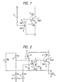
- Fig. 1 is an example of the basic circuit of the present invention.
- a transiently changing voltage is applied to the collector C and the emitter E (pair of main electrodes) of the IGBT 1 (the first semiconductor device)
- an electric displacement current flows through the capacitor 3 (the capacity element), the MOS gate (the control electrode) of a MOSFET 2 (the second semiconductor device) for a gate short-circuit and the source electrode (the second main electrode) between the settling electric potential V a and the emitter electrode E (one of the main electrodes) of the IGBT 1.
- the parasitic capacitances 8 and 9 are charged by the electric displacement current, and the state between the drain electrode (the first main electrode) and the source electrode of the MOSFET 2 becomes ON.
- the parasitic capacitances Cgc 6, Cge 7 are charged in the same way.
- the gate and the emitter of the MOS gate (the insulated gate electrode) IGBT 1 are short-circuited through the switching of the MOSFET 2 into the ON state, the electric charges of the parasitic capacitances are discharged through the MOSFET 2. Accordingly, the IGBT 1 is not switched on because the gate voltage of the IGBT does not rise.
- a protection circuit portion may be provided using a resistance element having a high resistance value or a high withstanding voltage. Accordingly, the chip area may be reduced.
- a circuit being an embodiment of the present invention is shown in Fig. 2.
- the operational conditions of the circuit are shown in Fig. 3, and the change thereof upon a transient change of the voltage, dV/dt, is shown in Fig. 4.
- a MOSFET is used as the capacity element, one end thereof is connected to the collector voltage of the IGBT 1.
- the IGBT 1 is ON.
- the switches 12, 16 are ON.
- the switch 16 supplies the voltage Vbb from a main power supply 17 to the gate G of the IGBT 1.
- the switch 12 With the switch 12 closed the electric charge accumulated between the gate and the source of the MOSFET 2 for a gate short-circuit is pulled up by a constant current source 14 and works to surely make the MOSFET 2 OFF.
- the switsch 13 is OFF in order to prevent an overlapping with the switch 16.
- the switch 12 is OFF, the switch 13 is ON, and the switch 16 is OFF.
- semicondcutor switching elements are used for these switches here.
- a constant current flows into a constant current source 15 through a Zener diode 18 by switching on the switch 13, and a reverse bias of approximately 0.7 V is added between the gate and the emitter of the IGBT 1.
- the gate of the MOSFET 2 transiently changes toward the voltage that is defined by the division ratio of the parasitic capacitance 11 of the N-MOSFET 10 to the parasitic capacity 8 (Cgd) and 9 (Cgs) of the MOSFET 2. However, it is clamped by the Zener voltage of the Zener diode 19.
- Fig. 4 shows the changes in the operation conditions when the voltage Va between the emitter of the IGBT 1 and the ground transiently descends from an arbitrary voltage Vx to 0 V.
- the initial condition of the electric charge of the parasitic capacities of 8 and 9 of the MOSFET 2 for gate short-circuit is defined as zero.
- the MOSFET 2 for the gate short-circuit when the MOSFET 2 for the gate short-circuit is provided, it turns on at tl, and the IGBT 1 is short-circuited, and then the parasitic capacity 7 is discharged, and the voltage between the gate and the emitter of the IGBT 1 does not reach the threshold voltage level so as not to turn on the IGBT 1. Accordingly, false operation or malfunction because of a transient voltage dV/dt may be prevented.
- the capacitance element of this embodiment a power loss can hardly occur, or, is pretty small compared to the case of using a resistance element. Therefore, according to this embodiment, the electric power consumption can be reduced. Furthermore, because this embodiment uses the capacitance of the MOSFET 10 as the capacitance element, if applied to an integrated circuit, the size of the chip can be reduced too.
- FIG. 5 Another embodiment of the present invention is shown in Fig. 5.
- the N-MOSFET 10 is used as the capacitance element in this embodiment too, one end thereof being connected to the voltage of the power supply for gate drive. That is, a power supply 20 for driving the gate of the IGBT 1 is connected to the higher potential side of the main power supply 17, and the drain of the N-MOSFET 10 is connected to the higher potential side of the power supply 20 for driving the gate of this IGBT 1.
- the MOSFET used as the capacitance element for malfunction prevention is connected to the gate circuit side, any interference between the main circuit side and the gate circuit side through this capacitance element is hard to happen.
- the circuit of this embodiment is constructed in the form of a monolithic circuit comprised in the semiconductor chip, it becomes easy to design the layout of the element as the main circuit part and the gate circuit part do not interfere with each other.
- Fig. 6 shows an embodiment of a monolithic inverter circuit 40 shown with a dotted line for driving a 3-phase brushless motor using the circuit shown in Fig. 5.
- the power supply 30 for driving the motor is a power supply for driving the 3-phase brushless motor 39 in which a hall element for detecting the magnetic pole position of the rotor is built in.
- the power supply 30 for driving the motor 39 is connected with a 3-phase bridge circuit which is constructed with the IGBTs 37a to 37f and free-running diodes 38a to 38f which are connected in direction in parallel to the main electrodes of the IGBTs 37a to 37f, respectively.
- the power supply 31 for the monolithic IC control is a power supply for driving a signal transformation circuit 33 which receives and divides the output signal from the gate drive circuits 36a to 36c of the IGBTs 37d to 37f of the lower arm and from the hall element provided in the motor 39.
- the power supply circuit 34 is a circuit for generating the voltage supplied to the gate drive circuits 35a to 35c of the upper arm IGBTs 37a to 37c. Accordingly, the apparatus constitution becomes simple because an external gate power supply for the upper arm becomes unnecessary.
- the control signal generating device 32 of the monolithic IC is a circuit for controlling the ON-OFF duty ratio of the IGBTs of each arm. The inner part encircled by the broken line is constructed with the monolithic IC 40 in the figure.
- the parts provided with a circuit shown in Fig. 5 in the above-mentioned circuit correspond to upper arm drive circuits 35a to 35c.
- the power supply 20 for driving the IGBT in Fig. 5 corresponds to the power supply 34 of this embodiment here.
- the circuit of Fig. 5 is suitable for use in inverter circuits as shown in Fig. 6.
- any malfunction of the IGBTs in the upper arm cannot arise even if a transient voltage dV/dt is applied by a chopping of the IGBTs 37a to 37f of the lower arm.
- Fig. 7 shows an example of the pattern layout of the monolithic IC 40 in Fig. 6.
- the symbols in this figure correspond to those in Fig. 6, and the upper arm drive circuit corresponds to the driving circuits 35a to 35c of the hatched part of Fig. 7.
- the malfunction prevention circuit as shown in Fig. 5 forms the driving circuits 35a to 35c. Accordingly, in the circuits using resistance elements in the conventional way, both chip size and electric power consumption thereof become pretty big, because a plurality of resistance elements having a high withstanding voltage and a high resistance value are necessary. On the contrary, in this embodiment, as the circuit is constructed with the capacitance of the MOSFET, the chip size and the electric power consumption can be reduced as compared to the conventional circuit arrangement.
- Fig. 8 shows a semiconductor circuit according to another embodiment of the present invention.
- a usual capacitor 3 (dielectric member provided between two metal electrodes) is connected. From the capacitor 3 an electric current flows only when a transient voltage dV/dt occurs between the collector C and the emitter E of the IGBT 1, and the parasitic capacitances Cgd 8, Cgd 9 between the gate and the drain and the source of the MOSFET 2 are charged so as to turn on the MOSFET 2.
- a switch SW 4 is provided between the gate and the drain of the MOSFET 2 for discharging the electric charge of the parasitic gate capacitances 8 and 9 of the MOSFET 2.
- the switch SW 4 a semiconductor switching element is used. According to a signal for controlling the switch 4 and the IGBT drive circuit 5, the IGBT 1 is turned off within a period for protecting the IGBT 1 from the transient voltage dV/dt during its OFF period, and is turned on within a period of ON state of the IGBT 1.
- the switching element of the main circuit is the IGBT, however, the present invention may be applied also to cases where an insulated gate type semiconductor device such as a MOSFET is used for the main circuit.
- the present invention may be applied to not only the inverter devices, but also to other apparatus in which a transient voltage dV/dt is applied to a switching element thereof.
- the circuit used in these apparatus is effective in cases where it is used not only as an integrated circuit, but also as a single body element or a modular construction.
- the circuit that consists of the semiconductor device for the gate short-circuit and the capacitance element operates as a kind of dV/dt detection circuit. Therefore, according to the output signal of such a detection circuit, malfunction of the main circuit semiconductor device may be prevented by putting out an OFF control signal from the drive circuit of the semiconductor device of the main circuit.
- the semiconductor circuit of the present invention because the operational behavior of the gate short-circuit, malfunctions of the semiconductor device are prevented only when a transient voltage dV/dt occurs; therefore, the electric power consumption is effectively reduced as compared with the conventional technology.
- monolithic semiconductor integrated circuits of the present invention lead to an effective reduction of the chip area because resistance elements of high withstanding voltage and of high resistance value requiring a big cell area are no longer necessary.
Landscapes
- Engineering & Computer Science (AREA)
- Power Engineering (AREA)
- Electronic Switches (AREA)
- Power Conversion In General (AREA)
- Inverter Devices (AREA)
- Semiconductor Integrated Circuits (AREA)
- Metal-Oxide And Bipolar Metal-Oxide Semiconductor Integrated Circuits (AREA)
Description
- The present invention relates to a semiconductor circuit utilizing a MOSFET and a semiconductor device of IGBT type and monolithic semiconductor integrated circuits comprising this circuit.
- As for the voltage drive type semiconductor devices such as insulated gate bipolar transistors (hereinafter called IGBT), MOS type field-effect transistors (hereinafter called MOSFETs), etc., high-speed switching thereof is possible. Therefore, the devices may be driven with a high frequency if the semiconductor device is for example applied to an inverter apparatus for driving a motor. Accordingly, size and weight of the devices and their noise development may be minimized. However, in high frequency inverter apparatus, when the semiconductor device is switched on and off, a large voltage change dV/dt is applied suddenly to the semiconductor device. Then the IGBT and the MOSFET may show malfunction and turn on in a period where they should be turned off originally. In this case, a short-circuit accident of the upper or the lower arm of the inverter apparatus may occur. And, in the case of monolithic semiconductor integrated circuits in which the circuit of the inverter apparatus is monolithically provided as one semiconductor chip, the semiconductor chip may be destroyed.
- A conventional technology for preventing such failures of semiconductor apparatus of this type is described in JP-A-63-99779 (1989) for example.
- This document shows a circuit for biasing the gate of the MOSFET by connecting the MOSFET between the gate and the emitter of the IGBT of the main circuit and by connecting the gate of the MOSFET to a power supply for driving the gate of the IGBT through a resistor element. By this circuit, when the IGBT is in the OFF state, the gate of the MOSFET biased, and the MOSFET is switched on, a short-circuit is provided between the gate and the emitter of the IGBT. Thereby, even if a large voltage change dV/dt is applied between the collector and the emitter of the IGBT, the IGBT does not show such a failure.
- However, in the conventional technology, when the IGBT is in the OFF state, the electric power consumption increases because the MOSFET is always set up as in the ON state. Furthermore, a resistor element having a high resistance value and a high withstand voltage becomes necessary, and the chip area becomes large when the inverter circuit is implemented in the form of a monolithic circuit.
- It is the underlying problem of the present invention to overcome the disadvantages of the prior art mentioned above and to provide a semiconductor circuit and its implementation in monolithic form, which leads to a lower electric power consumption of the circuit and a reduction of the chip area in the case of monolithics.
- The above problem is solved according to the independent claims. The dependent claims relate to preferred embodiments of the concept of the present invention.
- The semiconductor circuit of the present invention comprises a first semiconductor device having a pair of main electrodes and an insulated gate electrode, and a second semiconductor device having a first main electrode, a second main electrode and a control electrode. Here, the first main electrode of the second semiconductor device is connected to the insulated gate electrode of the first semiconductor device, and the second main electrode of the second semiconductor device is connected to one of the main electrodes of the first semiconductor device.
- A capacity element is connected between the control electrode of the second semiconductor device and an electric settling potential.
- In the integrated circuit of the present invention, the semiconductor circuit of the present invention described above is formed on the same semiconductor substrate.
- According to the semiconductor circuit of the present invention, when the voltage applied to the two main electrodes of the first semiconductor device changes, an electric displacement current flows in a capacity element. Because this electric displacement current is supplied as a control signal to the control electrode of the second semiconductor device, the second semiconductor device is turned on. By this the insulated gate electrode of the first semiconductor apparatus is short-circuited with one of its main electrodes, and therefore, turn-on of the first semiconductor device by a transient voltage dV/dt (failure, malfunction) may be prevented.
- In the following, the present invention will be explained with reference to the drawings.
- Fig. 1
- is an example of the basic circuit of the present invention.
- Fig. 2
- is the circuit constitution of one embodiment of the present invention.
- Fig. 3
- shows the operation conditions of the circuit shown in Fig. 2.
- Fig. 4
- shows the operational conditions of the circuit shown in Fig. 2 when a transient voltage change arises.
- Fig. 5
- is another embodiment according to the present invention.
- Fig. 6
- is an embodiment of a monolithic inverter circuit for driving a three phase brushless motor using the circuit shown in Fig. 5.
- Fig. 7
- is an example of the pattern layout of the monolithic IC shown in Fig. 6.
- Fig. 8
- ist another embodiment according to the present invention.
- The operation of the semiconductor circuit of the present invention will be explained with reference to Fig. 1.
- Fig. 1 is an example of the basic circuit of the present invention. When a transiently changing voltage is applied to the collector C and the emitter E (pair of main electrodes) of the IGBT 1 (the first semiconductor device), an electric displacement current flows through the capacitor 3 (the capacity element), the MOS gate (the control electrode) of a MOSFET 2 (the second semiconductor device) for a gate short-circuit and the source electrode (the second main electrode) between the settling electric potential Va and the emitter electrode E (one of the main electrodes) of the
IGBT 1. Theparasitic capacitances MOSFET 2 becomes ON. On the other hand, in theIGBT 1, theparasitic capacitances Cgc 6,Cge 7 are charged in the same way. However, as the gate and the emitter of the MOS gate (the insulated gate electrode)IGBT 1 are short-circuited through the switching of theMOSFET 2 into the ON state, the electric charges of the parasitic capacitances are discharged through theMOSFET 2. Accordingly, theIGBT 1 is not switched on because the gate voltage of the IGBT does not rise. - As the electric displacement current flows only when the voltage chages, the electric power consumption of the circuit is reduced.
- Further, according to the integrated circuit of the present invention where the semiconductor circuit of the present invention is provided on a semiconductor substrate, a protection circuit portion may be provided using a resistance element having a high resistance value or a high withstanding voltage. Accordingly, the chip area may be reduced.
- The constitution of a circuit being an embodiment of the present invention is shown in Fig. 2. The operational conditions of the circuit are shown in Fig. 3, and the change thereof upon a transient change of the voltage, dV/dt, is shown in Fig. 4.
- In this embodiment, a MOSFET is used as the capacity element, one end thereof is connected to the collector voltage of the
IGBT 1. - At first, the operation will be explained when the
IGBT 1 is ON. As shown in the waveform diagrams of Fig. 3, theswitches switch 16 supplies the voltage Vbb from amain power supply 17 to the gate G of theIGBT 1. With theswitch 12 closed the electric charge accumulated between the gate and the source of theMOSFET 2 for a gate short-circuit is pulled up by a constantcurrent source 14 and works to surely make theMOSFET 2 OFF. Theswitsch 13 is OFF in order to prevent an overlapping with theswitch 16. - The changes will now be explained when the IGBT 1 is switched OFF next. In the circuit operation conditions shown in Fig. 3, the
switch 12 is OFF, theswitch 13 is ON, and theswitch 16 is OFF. Actually, semicondcutor switching elements are used for these switches here. A constant current flows into a constant current source 15 through a Zenerdiode 18 by switching on theswitch 13, and a reverse bias of approximately 0.7 V is added between the gate and the emitter of theIGBT 1. On the other hand, as theswitch 12 is OFF, the gate of theMOSFET 2 transiently changes toward the voltage that is defined by the division ratio of theparasitic capacitance 11 of the N-MOSFET 10 to the parasitic capacity 8 (Cgd) and 9 (Cgs) of theMOSFET 2. However, it is clamped by the Zener voltage of the Zenerdiode 19. - Fig. 4 shows the changes in the operation conditions when the voltage Va between the emitter of the
IGBT 1 and the ground transiently descends from an arbitrary voltage Vx to 0 V. Here, the initial condition of the electric charge of the parasitic capacities of 8 and 9 of theMOSFET 2 for gate short-circuit is defined as zero. When, in Fig. 4, a descent of the voltage occured at the time point of tO, theparasitic capacitance 1 and theparasitic capacities MOSFET 2 for the gate short-circuit are started to be charged with the electric charge, the voltage between the gate and the source of theMOSFET 2 rising as shown in Fig. 4 (b). When this voltage is increased up to the threshold level (Vth1) of theMOSFET 2, theMOSFET 2 is switched on. On the other hand, as shown in Fig. 4 (c), the voltage between the gate and the emitter of theIGBT 1 rises in the same way by charging the parasitic capacity of 6 (Cgc) and 7 (Cge) with electric charge. If theMOSFET 2 is not provided, then the voltage between the gate and the emitter of theIGBT 1 changes like the dotted line of Fig. 4 (c), exceeds the threshold voltage level (Vth2) of the gate of theIGBT 1, and theIGBT 1 turns on. On the other hand, when theMOSFET 2 for the gate short-circuit is provided, it turns on at tl, and theIGBT 1 is short-circuited, and then theparasitic capacity 7 is discharged, and the voltage between the gate and the emitter of theIGBT 1 does not reach the threshold voltage level so as not to turn on theIGBT 1. Accordingly, false operation or malfunction because of a transient voltage dV/dt may be prevented. - In the capacitance element of this embodiment, a power loss can hardly occur, or, is pretty small compared to the case of using a resistance element. Therefore, according to this embodiment, the electric power consumption can be reduced. Furthermore, because this embodiment uses the capacitance of the
MOSFET 10 as the capacitance element, if applied to an integrated circuit, the size of the chip can be reduced too. - Another embodiment of the present invention is shown in Fig. 5. The N-
MOSFET 10 is used as the capacitance element in this embodiment too, one end thereof being connected to the voltage of the power supply for gate drive. That is, apower supply 20 for driving the gate of theIGBT 1 is connected to the higher potential side of themain power supply 17, and the drain of the N-MOSFET 10 is connected to the higher potential side of thepower supply 20 for driving the gate of thisIGBT 1. - In the following, the change of the operation conditions of this embodiment will be explained when a transient voltage change dV/dt is generated. When the
IGBT 1 is in the OFF state, theswitches switch 13 is ON in the same way as in Fig. 2. Theparasitic capacitance 11 of the N-MOSFET 10 is charged by a voltage of [(the voltage of themain power supply 17 + the voltage of thepower supply 20 for driving the IGBT)-(Va + Zener voltage of the Zener diode 19)]. When the voltage change dV/dt is generated, the change in the operation conditions is similar as in the case of the former embodiment. - In this embodiment, because the MOSFET used as the capacitance element for malfunction prevention is connected to the gate circuit side, any interference between the main circuit side and the gate circuit side through this capacitance element is hard to happen. On this account, when the circuit of this embodiment is constructed in the form of a monolithic circuit comprised in the semiconductor chip, it becomes easy to design the layout of the element as the main circuit part and the gate circuit part do not interfere with each other.
- Fig. 6 shows an embodiment of a
monolithic inverter circuit 40 shown with a dotted line for driving a 3-phase brushless motor using the circuit shown in Fig. 5. In Fig. 6, thepower supply 30 for driving the motor is a power supply for driving the 3-phase brushless motor 39 in which a hall element for detecting the magnetic pole position of the rotor is built in. Thepower supply 30 for driving themotor 39 is connected with a 3-phase bridge circuit which is constructed with the IGBTs 37a to 37f and free-runningdiodes 38a to 38f which are connected in direction in parallel to the main electrodes of the IGBTs 37a to 37f, respectively. Thepower supply 31 for the monolithic IC control is a power supply for driving asignal transformation circuit 33 which receives and divides the output signal from thegate drive circuits 36a to 36c of theIGBTs 37d to 37f of the lower arm and from the hall element provided in themotor 39. Thepower supply circuit 34 is a circuit for generating the voltage supplied to thegate drive circuits 35a to 35c of theupper arm IGBTs 37a to 37c. Accordingly, the apparatus constitution becomes simple because an external gate power supply for the upper arm becomes unnecessary. Further, the controlsignal generating device 32 of the monolithic IC is a circuit for controlling the ON-OFF duty ratio of the IGBTs of each arm. The inner part encircled by the broken line is constructed with themonolithic IC 40 in the figure. - The parts provided with a circuit shown in Fig. 5 in the above-mentioned circuit correspond to upper
arm drive circuits 35a to 35c. Thepower supply 20 for driving the IGBT in Fig. 5 corresponds to thepower supply 34 of this embodiment here. In other words, the circuit of Fig. 5 is suitable for use in inverter circuits as shown in Fig. 6. In this embodiment with the bridge constitution as shown in Fig. 6, any malfunction of the IGBTs in the upper arm cannot arise even if a transient voltage dV/dt is applied by a chopping of the IGBTs 37a to 37f of the lower arm. - Fig. 7 shows an example of the pattern layout of the
monolithic IC 40 in Fig. 6. The symbols in this figure correspond to those in Fig. 6, and the upper arm drive circuit corresponds to the drivingcircuits 35a to 35c of the hatched part of Fig. 7. The malfunction prevention circuit as shown in Fig. 5 forms the drivingcircuits 35a to 35c. Accordingly, in the circuits using resistance elements in the conventional way, both chip size and electric power consumption thereof become pretty big, because a plurality of resistance elements having a high withstanding voltage and a high resistance value are necessary. On the contrary, in this embodiment, as the circuit is constructed with the capacitance of the MOSFET, the chip size and the electric power consumption can be reduced as compared to the conventional circuit arrangement. - Fig. 8 shows a semiconductor circuit according to another embodiment of the present invention. Between the gate of the
MOSFET 2 and the collector C of theIBGT 1, a usual capacitor 3 (dielectric member provided between two metal electrodes) is connected. From thecapacitor 3 an electric current flows only when a transient voltage dV/dt occurs between the collector C and the emitter E of theIGBT 1, and the parasitic capacitances Cgd 8,Cgd 9 between the gate and the drain and the source of theMOSFET 2 are charged so as to turn on theMOSFET 2. As means for turning off theMOSFET 2 for gate short-circuit, in addition to the above measures, a switch SW 4 is provided between the gate and the drain of theMOSFET 2 for discharging the electric charge of theparasitic gate capacitances MOSFET 2. As the switch SW 4, a semiconductor switching element is used. According to a signal for controlling the switch 4 and theIGBT drive circuit 5, theIGBT 1 is turned off within a period for protecting theIGBT 1 from the transient voltage dV/dt during its OFF period, and is turned on within a period of ON state of theIGBT 1. - In the above-mentioned embodiment, the switching element of the main circuit is the IGBT, however, the present invention may be applied also to cases where an insulated gate type semiconductor device such as a MOSFET is used for the main circuit.
- In addition, the present invention may be applied to not only the inverter devices, but also to other apparatus in which a transient voltage dV/dt is applied to a switching element thereof. Furthermore, the circuit used in these apparatus is effective in cases where it is used not only as an integrated circuit, but also as a single body element or a modular construction.
- In addition to the above, in the present invention, the circuit that consists of the semiconductor device for the gate short-circuit and the capacitance element operates as a kind of dV/dt detection circuit. Therefore, according to the output signal of such a detection circuit, malfunction of the main circuit semiconductor device may be prevented by putting out an OFF control signal from the drive circuit of the semiconductor device of the main circuit.
- According to the semiconductor circuit of the present invention, because the operational behavior of the gate short-circuit, malfunctions of the semiconductor device are prevented only when a transient voltage dV/dt occurs; therefore, the electric power consumption is effectively reduced as compared with the conventional technology.
- In addition thereto, monolithic semiconductor integrated circuits of the present invention lead to an effective reduction of the chip area because resistance elements of high withstanding voltage and of high resistance value requiring a big cell area are no longer necessary.
Claims (13)
- Semiconductor circuit comprising:a first voltage drive type semiconductor device (IGBT, 1) having a pair of main electrodes (C, E) and an insulated gate electrode (G),a second voltage drive type semiconductor device (MOSFET, 2) having a first main electrode, a second main electrode and a control electrode, the first main electrode being connected to the insulated gate electrode (G) of the first voltage drive type semiconductor device (IGBT, 1), and the second main electrode being connected to one of the main electrodes (E) of the first voltage drive type semiconductor device (IGBT, 1), anda capacity element (3) connected between the control electrode of the voltage drive type second semiconductor device (MOSFET, 2) and an electric settling potential (Va), whereby the second voltage drive type semiconductor device (MOSFET, 2) is turned on.
- Semiconductor circuit according to claim 1,
characterized in that
the electric settling potential (Va) is applied to the other main electrode (E) of the first voltage drive type semiconductor device (IGBT, 1). - Semiconductor circuit according to claim 1,
characterized in that
the electric settling potential is applied to a driving circuit of the first voltage drive type semiconductor device (IGBT, 1). - Semiconductor circuit according to any of claims 1 to 3,
characterized in that
the capacity element (3) is constructed with a MOS type field-effect transistor (10). - Semiconductor circuit according to any of claims 1 to 3,
characterized in that
the capacity element (3) is a capacitor. - Semiconductor circuit according to any of claims 1 to 5,
characterized in that
the first voltage drive type semiconductor device (IGBT, 1) is an insulated gate bi-polar transistor. - Semiconductor circuit according to any of claims 1 to 5,
characterized in that
the first voltage drive type semiconductor device is a MOS type field-effect transistor. - Semiconductor circuit according to any of claims 1 to 7,
characterized in that
the second voltage drive type semiconductor device is a MOS type field-effect transistor (MOSFET, 2). - Semiconductor circuit according to any of claims 1 to 7,
characterized in that
the second voltage drive type semiconductor device is an insulated gate bi-polar transistor. - Semiconductor circuit, comprising:a plurality of first voltage drive type semiconductor devices connected in series and connected to a direct current power supply having a pair of main electrodes and an insulated gate electrode, wherein an output is taken out from the series connection point of the first voltage drive type semiconductor devices,a second voltage drive type semiconductor device having a first main electrode, a second main electrode and a control electrode, the first main electrode being connected to the insulated gate electrode of at least one of the first voltage drive type semiconductor devices, and the second main electrode being connected to one of the main electrodes of one of the voltage drive type first semiconductor devices, anda capacity element connected between the control electrode of the voltage drive type second semiconductor device and an electric settling electric potential, whereby the second voltage drive type semiconductor device (MOSFET, 2) is turned on.
- Inverter circuit, comprising one or a plurality of semiconductor circuits according to one of claims 1 to 10.
- Monolithic semiconductor circuit, characterized by one or a plurality of semiconductor circuits according to one of claims 1 to 10 or one or a plurality of inverter circuits according to claim 11, provided on the same semiconductor substrate.
- Use of the semiconductor circuits according to claims 1 to 12 for apparatus comprising one or a plurality of semiconductor switching devices for protection of the semiconductor switching devices against failure or malfunction through gate short-circuit in the case of occurrence of a dangerous transient voltage (dV/dt).
Applications Claiming Priority (3)
| Application Number | Priority Date | Filing Date | Title |
|---|---|---|---|
| JP224753/94 | 1994-09-20 | ||
| JP22475394 | 1994-09-20 | ||
| JP22475394A JP3222330B2 (en) | 1994-09-20 | 1994-09-20 | Semiconductor circuit and semiconductor integrated circuit |
Publications (3)
| Publication Number | Publication Date |
|---|---|
| EP0703664A2 EP0703664A2 (en) | 1996-03-27 |
| EP0703664A3 EP0703664A3 (en) | 1996-09-18 |
| EP0703664B1 true EP0703664B1 (en) | 2002-12-04 |
Family
ID=16818703
Family Applications (1)
| Application Number | Title | Priority Date | Filing Date |
|---|---|---|---|
| EP95114786A Expired - Lifetime EP0703664B1 (en) | 1994-09-20 | 1995-09-20 | Semiconductor circuit |
Country Status (4)
| Country | Link |
|---|---|
| US (1) | US5818281A (en) |
| EP (1) | EP0703664B1 (en) |
| JP (1) | JP3222330B2 (en) |
| DE (1) | DE69529042T2 (en) |
Cited By (1)
| Publication number | Priority date | Publication date | Assignee | Title |
|---|---|---|---|---|
| DE102004063536A1 (en) * | 2004-12-30 | 2006-07-20 | Mitsubishi Denki K.K. | Inverter circuit includes noise suppression circuit to set zero impedance between control terminal and main terminals of switch according to detection of variation in amplitude and frequency of drive voltage |
Families Citing this family (45)
| Publication number | Priority date | Publication date | Assignee | Title |
|---|---|---|---|---|
| JPH10321855A (en) * | 1997-03-18 | 1998-12-04 | Toshiba Corp | High voltage semiconductor device |
| JP3067687B2 (en) * | 1997-05-08 | 2000-07-17 | 富士電機株式会社 | IGBT drive circuit |
| DE19842045B4 (en) * | 1998-09-14 | 2006-02-02 | Siemens Ag | Protection method for a controllable non-latching semiconductor switching element and protective circuit corresponding thereto |
| DE19849097A1 (en) * | 1998-10-24 | 2000-04-27 | Abb Daimler Benz Transp | Method for switching status monitoring of an IGBT and device for carrying out the method |
| DE60042392D1 (en) | 2000-01-20 | 2009-07-30 | St Microelectronics Srl | Power device with protection against unwanted self-activation |
| KR200229676Y1 (en) * | 2000-11-14 | 2001-07-19 | 엘지산전 주식회사 | Circuit of driving gate of igbt inverter |
| DE20104111U1 (en) * | 2001-03-08 | 2002-07-18 | iC-Haus GmbH, 55294 Bodenheim | Circuit arrangement for overcurrent free switching on and off of a current |
| JP2002290224A (en) * | 2001-03-23 | 2002-10-04 | Tdk Corp | Semiconductor element |
| JP3788926B2 (en) * | 2001-10-19 | 2006-06-21 | 三菱電機株式会社 | Semiconductor device and transistor driving method |
| JP2004014547A (en) * | 2002-06-03 | 2004-01-15 | Toshiba Corp | Semiconductor device and capacitance adjusting circuit |
| JP4084117B2 (en) * | 2002-07-26 | 2008-04-30 | 株式会社ルネサステクノロジ | Motor drive device |
| JP2004112987A (en) * | 2002-07-26 | 2004-04-08 | Fuji Electric Holdings Co Ltd | Power converter |
| JP2004215493A (en) * | 2002-12-20 | 2004-07-29 | Matsushita Electric Ind Co Ltd | Gate driver, motor driving device including the gate driver, and device including the motor driving device |
| JP3733122B2 (en) * | 2003-03-27 | 2006-01-11 | 株式会社ディーブイイー | Stabilized power circuit |
| JP3733121B2 (en) * | 2003-03-27 | 2006-01-11 | 株式会社ディーブイイー | Stabilized power circuit |
| US7142040B2 (en) | 2003-03-27 | 2006-11-28 | Device Engineering Co., Ltd. | Stabilized power supply circuit |
| US7542258B2 (en) * | 2004-01-16 | 2009-06-02 | Lutron Electronics Co., Inc. | DV/dt-detecting overcurrent protection circuit for power supply |
| JP4477952B2 (en) * | 2004-07-09 | 2010-06-09 | 株式会社ルネサステクノロジ | Semiconductor device, DC / DC converter and power supply system |
| US7660094B2 (en) * | 2004-12-14 | 2010-02-09 | Mitsubishi Denki Kabushiki Kaisha | Inverter circuit |
| FR2880481B1 (en) * | 2005-01-06 | 2007-03-30 | Mitsubishi Electric Corp | INVERTER CIRCUIT |
| JP4770304B2 (en) * | 2005-07-12 | 2011-09-14 | 富士電機株式会社 | Semiconductor device gate drive circuit |
| KR100687936B1 (en) | 2005-11-29 | 2007-02-27 | 삼성전자주식회사 | Electronic device and power circuit |
| DE102006059833B4 (en) * | 2006-12-15 | 2016-12-01 | Sew-Eurodrive Gmbh & Co Kg | Electric device |
| JP2009224667A (en) * | 2008-03-18 | 2009-10-01 | Fujitsu Telecom Networks Ltd | Field effect transistor, semiconductor device, control circuit, control method therefor, and insulated gate bipolar transistor |
| JP5492518B2 (en) * | 2009-10-02 | 2014-05-14 | 株式会社日立製作所 | Semiconductor drive circuit and semiconductor device using the same |
| US20110148376A1 (en) * | 2009-12-23 | 2011-06-23 | Texas Instruments Incorporated | Mosfet with gate pull-down |
| GB2479372B (en) * | 2010-04-07 | 2013-07-24 | Ge Aviat Systems Ltd | Power switches for aircraft |
| JP2011228372A (en) * | 2010-04-16 | 2011-11-10 | Toshiba Corp | Semiconductor integrated circuit device |
| JP2015142155A (en) * | 2014-01-27 | 2015-08-03 | 株式会社デンソー | semiconductor device module and gate drive circuit |
| JP5928417B2 (en) * | 2013-07-30 | 2016-06-01 | 株式会社デンソー | Semiconductor element module and gate drive circuit |
| US9094005B2 (en) * | 2013-07-30 | 2015-07-28 | Denso Corporation | Semiconductor element module and gate drive circuit |
| EP2849323B1 (en) * | 2013-09-17 | 2016-04-20 | Dialog Semiconductor GmbH | Control circuit for multiple high side switches |
| EP2908339A1 (en) * | 2014-02-17 | 2015-08-19 | ABB Technology AG | Power semiconductor arrangement and method for protecting a power semiconductor module against failures |
| DE102015110423B4 (en) | 2015-06-29 | 2023-01-05 | Halla Visteon Climate Control Corporation | Power electronics assembly to prevent parasitic turn-on of circuit breakers |
| JP6894957B2 (en) * | 2015-10-07 | 2021-06-30 | ローム株式会社 | False output prevention circuit |
| JP6591315B2 (en) * | 2016-03-09 | 2019-10-16 | ルネサスエレクトロニクス株式会社 | Semiconductor device, charge pump circuit, semiconductor system, vehicle, and control method of semiconductor device |
| CN110768649B (en) * | 2018-07-26 | 2023-03-24 | 台达电子工业股份有限公司 | Gate circuit and gate drive circuit of power semiconductor switch |
| JP7406520B2 (en) * | 2021-03-22 | 2023-12-27 | 株式会社 日立パワーデバイス | Upper arm drive circuit, power conversion device drive circuit, power conversion device |
| EP4092740B1 (en) | 2021-05-21 | 2025-06-25 | Infineon Technologies Austria AG | Semiconductor die with a vertical transistor device |
| US11936383B2 (en) * | 2021-12-01 | 2024-03-19 | Tagore Technology, Inc. | Bias-less dynamic miller clamp |
| US12574025B2 (en) * | 2023-01-17 | 2026-03-10 | Analog Devices, Inc. | Transistor assemblies with gate current shunting capability, and associated methods |
| JPWO2024189895A1 (en) * | 2023-03-16 | 2024-09-19 | ||
| JP2024158299A (en) * | 2023-04-27 | 2024-11-08 | ミネベアパワーデバイス株式会社 | Upper arm drive circuit and power conversion device |
| WO2025009016A1 (en) * | 2023-07-03 | 2025-01-09 | 三菱電機株式会社 | Electric power conversion apparatus |
| US20250330168A1 (en) * | 2024-04-18 | 2025-10-23 | Apple Inc. | Self-Biased Power Switching Circuitry |
Family Cites Families (18)
| Publication number | Priority date | Publication date | Assignee | Title |
|---|---|---|---|---|
| US3819952A (en) * | 1973-01-29 | 1974-06-25 | Mitsubishi Electric Corp | Semiconductor device |
| US3909674A (en) * | 1974-03-28 | 1975-09-30 | Rockwell International Corp | Protection circuit for MOS driver |
| JPS585526B2 (en) * | 1974-07-19 | 1983-01-31 | 株式会社日立製作所 | Hand tie switch |
| JPS5647704B2 (en) * | 1974-07-26 | 1981-11-11 | ||
| US4084110A (en) * | 1975-10-01 | 1978-04-11 | Hitachi, Ltd. | Semiconductor switch |
| JPS5418664A (en) * | 1977-07-13 | 1979-02-10 | Hitachi Ltd | Semiconductor switch |
| US4551643A (en) * | 1983-10-24 | 1985-11-05 | Rca Corporation | Power switching circuitry |
| JPS60112318A (en) * | 1983-11-22 | 1985-06-18 | Nec Corp | Semiconductor integrated circuit switch |
| JPS60167522A (en) * | 1984-02-10 | 1985-08-30 | Hitachi Ltd | Semiconductor switch |
| JPS6399779A (en) * | 1986-10-13 | 1988-05-02 | Fuji Electric Co Ltd | Power converter |
| JPS63187815A (en) * | 1987-01-30 | 1988-08-03 | Hitachi Ltd | semiconductor switch |
| US5055721A (en) * | 1989-04-13 | 1991-10-08 | Mitsubishi Denki Kabushiki Kaisha | Drive circuit for igbt device |
| JPH07112150B2 (en) * | 1989-04-28 | 1995-11-29 | 株式会社東芝 | Optical trigger switching circuit |
| DE58907470D1 (en) * | 1989-07-17 | 1994-05-19 | Siemens Ag | Zero point detector for an optically controllable thyristor. |
| US4992683A (en) * | 1989-09-28 | 1991-02-12 | Motorola, Inc. | Load driver with reduced dissipation under reverse-battery conditions |
| JPH05122035A (en) * | 1991-05-10 | 1993-05-18 | Fuji Electric Co Ltd | Semiconductor device with built-in driving power source |
| JP2956319B2 (en) * | 1991-11-07 | 1999-10-04 | 富士電機株式会社 | Reverse bias control circuit for voltage driven switching element |
| US5434527A (en) * | 1993-10-25 | 1995-07-18 | Caterpillar Inc. | Gate drive circuit |
-
1994
- 1994-09-20 JP JP22475394A patent/JP3222330B2/en not_active Expired - Lifetime
-
1995
- 1995-09-15 US US08/528,887 patent/US5818281A/en not_active Expired - Fee Related
- 1995-09-20 DE DE69529042T patent/DE69529042T2/en not_active Expired - Fee Related
- 1995-09-20 EP EP95114786A patent/EP0703664B1/en not_active Expired - Lifetime
Cited By (2)
| Publication number | Priority date | Publication date | Assignee | Title |
|---|---|---|---|---|
| DE102004063536A1 (en) * | 2004-12-30 | 2006-07-20 | Mitsubishi Denki K.K. | Inverter circuit includes noise suppression circuit to set zero impedance between control terminal and main terminals of switch according to detection of variation in amplitude and frequency of drive voltage |
| DE102004063536B4 (en) * | 2004-12-30 | 2013-11-21 | Mitsubishi Denki K.K. | converter |
Also Published As
| Publication number | Publication date |
|---|---|
| US5818281A (en) | 1998-10-06 |
| DE69529042T2 (en) | 2003-10-09 |
| EP0703664A2 (en) | 1996-03-27 |
| DE69529042D1 (en) | 2003-01-16 |
| JP3222330B2 (en) | 2001-10-29 |
| EP0703664A3 (en) | 1996-09-18 |
| JPH0888550A (en) | 1996-04-02 |
Similar Documents
| Publication | Publication Date | Title |
|---|---|---|
| EP0703664A2 (en) | Semiconductor circuit comprising means for malfunction prevention, and its use, particularly for inverters | |
| KR100341702B1 (en) | Circuit for driving a half-bridge | |
| US6781422B1 (en) | Capacitive high-side switch driver for a power converter | |
| US6215634B1 (en) | Drive circuit for power device | |
| EP0397241B1 (en) | Driver for high voltage half-bridge circuits | |
| US8299841B2 (en) | Semiconductor device | |
| JP2988859B2 (en) | Power MOSFET | |
| US4890020A (en) | Circuit for driving a semiconductor device with protection against transients | |
| JP7052452B2 (en) | Semiconductor device | |
| US20020014905A1 (en) | Level shift circuit | |
| JPH02266712A (en) | Semiconductor device | |
| JPH1032476A (en) | Overcurrent protection circuit | |
| JPH0671200B2 (en) | Power MOSFET protection circuit for driving inductive load | |
| JP2022077909A (en) | Semiconductor device | |
| JP4501178B2 (en) | Protective device for semiconductor device | |
| US5719420A (en) | Insulated gate type semiconductor device having built-in protection circuit | |
| EP0542460B1 (en) | Reverse-bias control circuit for a voltage-drive switching element | |
| KR20040029082A (en) | Half-bridge circuit | |
| US5726478A (en) | Integrated power semiconductor component having a substrate with a protective structure in the substrate | |
| EP0920114B1 (en) | Power converter wherein mos gate semiconductor device is used | |
| JP2023140714A (en) | semiconductor equipment | |
| EP0614278B1 (en) | Drive circuit for use with voltage-driven semiconductor device | |
| US12191790B2 (en) | Power module with protection circuit | |
| JPWO1998053546A1 (en) | Power conversion device using MOS gate type semiconductor element | |
| US20250096793A1 (en) | Switching control circuit |
Legal Events
| Date | Code | Title | Description |
|---|---|---|---|
| PUAI | Public reference made under article 153(3) epc to a published international application that has entered the european phase |
Free format text: ORIGINAL CODE: 0009012 |
|
| AK | Designated contracting states |
Kind code of ref document: A2 Designated state(s): DE SE |
|
| PUAL | Search report despatched |
Free format text: ORIGINAL CODE: 0009013 |
|
| AK | Designated contracting states |
Kind code of ref document: A3 Designated state(s): DE SE |
|
| 17P | Request for examination filed |
Effective date: 19960808 |
|
| GRAG | Despatch of communication of intention to grant |
Free format text: ORIGINAL CODE: EPIDOS AGRA |
|
| 17Q | First examination report despatched |
Effective date: 20011026 |
|
| GRAG | Despatch of communication of intention to grant |
Free format text: ORIGINAL CODE: EPIDOS AGRA |
|
| GRAG | Despatch of communication of intention to grant |
Free format text: ORIGINAL CODE: EPIDOS AGRA |
|
| GRAH | Despatch of communication of intention to grant a patent |
Free format text: ORIGINAL CODE: EPIDOS IGRA |
|
| RTI1 | Title (correction) |
Free format text: SEMICONDUCTOR CIRCUIT |
|
| GRAH | Despatch of communication of intention to grant a patent |
Free format text: ORIGINAL CODE: EPIDOS IGRA |
|
| GRAA | (expected) grant |
Free format text: ORIGINAL CODE: 0009210 |
|
| AK | Designated contracting states |
Kind code of ref document: B1 Designated state(s): DE SE |
|
| RIN1 | Information on inventor provided before grant (corrected) |
Inventor name: SHOICHI, OZEKI Inventor name: KOJI, KAWAMOTO Inventor name: HITOSHI, OHURA |
|
| REF | Corresponds to: |
Ref document number: 69529042 Country of ref document: DE Date of ref document: 20030116 |
|
| PLBE | No opposition filed within time limit |
Free format text: ORIGINAL CODE: 0009261 |
|
| STAA | Information on the status of an ep patent application or granted ep patent |
Free format text: STATUS: NO OPPOSITION FILED WITHIN TIME LIMIT |
|
| 26N | No opposition filed |
Effective date: 20030905 |
|
| PGFP | Annual fee paid to national office [announced via postgrant information from national office to epo] |
Ref country code: SE Payment date: 20080626 Year of fee payment: 14 |
|
| PGFP | Annual fee paid to national office [announced via postgrant information from national office to epo] |
Ref country code: DE Payment date: 20080908 Year of fee payment: 14 |
|
| EUG | Se: european patent has lapsed | ||
| PG25 | Lapsed in a contracting state [announced via postgrant information from national office to epo] |
Ref country code: DE Free format text: LAPSE BECAUSE OF NON-PAYMENT OF DUE FEES Effective date: 20100401 |
|
| PG25 | Lapsed in a contracting state [announced via postgrant information from national office to epo] |
Ref country code: SE Free format text: LAPSE BECAUSE OF NON-PAYMENT OF DUE FEES Effective date: 20090921 |