EP0702272A1 - Belichtungsapparat und Belichtungsverfahren - Google Patents
Belichtungsapparat und Belichtungsverfahren Download PDFInfo
- Publication number
- EP0702272A1 EP0702272A1 EP95306182A EP95306182A EP0702272A1 EP 0702272 A1 EP0702272 A1 EP 0702272A1 EP 95306182 A EP95306182 A EP 95306182A EP 95306182 A EP95306182 A EP 95306182A EP 0702272 A1 EP0702272 A1 EP 0702272A1
- Authority
- EP
- European Patent Office
- Prior art keywords
- exposure
- semiconductor substrate
- alignment
- data
- positions
- Prior art date
- Legal status (The legal status is an assumption and is not a legal conclusion. Google has not performed a legal analysis and makes no representation as to the accuracy of the status listed.)
- Granted
Links
Images


Classifications
-
- G—PHYSICS
- G03—PHOTOGRAPHY; CINEMATOGRAPHY; ANALOGOUS TECHNIQUES USING WAVES OTHER THAN OPTICAL WAVES; ELECTROGRAPHY; HOLOGRAPHY
- G03F—PHOTOMECHANICAL PRODUCTION OF TEXTURED OR PATTERNED SURFACES, e.g. FOR PRINTING, FOR PROCESSING OF SEMICONDUCTOR DEVICES; MATERIALS THEREFOR; ORIGINALS THEREFOR; APPARATUS SPECIALLY ADAPTED THEREFOR
- G03F9/00—Registration or positioning of originals, masks, frames, photographic sheets or textured or patterned surfaces, e.g. automatically
- G03F9/70—Registration or positioning of originals, masks, frames, photographic sheets or textured or patterned surfaces, e.g. automatically for microlithography
- G03F9/7003—Alignment type or strategy, e.g. leveling, global alignment
-
- G—PHYSICS
- G03—PHOTOGRAPHY; CINEMATOGRAPHY; ANALOGOUS TECHNIQUES USING WAVES OTHER THAN OPTICAL WAVES; ELECTROGRAPHY; HOLOGRAPHY
- G03F—PHOTOMECHANICAL PRODUCTION OF TEXTURED OR PATTERNED SURFACES, e.g. FOR PRINTING, FOR PROCESSING OF SEMICONDUCTOR DEVICES; MATERIALS THEREFOR; ORIGINALS THEREFOR; APPARATUS SPECIALLY ADAPTED THEREFOR
- G03F7/00—Photomechanical, e.g. photolithographic, production of textured or patterned surfaces, e.g. printing surfaces; Materials therefor, e.g. comprising photoresists; Apparatus specially adapted therefor
- G03F7/20—Exposure; Apparatus therefor
-
- G—PHYSICS
- G03—PHOTOGRAPHY; CINEMATOGRAPHY; ANALOGOUS TECHNIQUES USING WAVES OTHER THAN OPTICAL WAVES; ELECTROGRAPHY; HOLOGRAPHY
- G03F—PHOTOMECHANICAL PRODUCTION OF TEXTURED OR PATTERNED SURFACES, e.g. FOR PRINTING, FOR PROCESSING OF SEMICONDUCTOR DEVICES; MATERIALS THEREFOR; ORIGINALS THEREFOR; APPARATUS SPECIALLY ADAPTED THEREFOR
- G03F7/00—Photomechanical, e.g. photolithographic, production of textured or patterned surfaces, e.g. printing surfaces; Materials therefor, e.g. comprising photoresists; Apparatus specially adapted therefor
- G03F7/70—Microphotolithographic exposure; Apparatus therefor
- G03F7/70425—Imaging strategies, e.g. for increasing throughput or resolution, printing product fields larger than the image field or compensating lithography- or non-lithography errors, e.g. proximity correction, mix-and-match, stitching or double patterning
- G03F7/70433—Layout for increasing efficiency or for compensating imaging errors, e.g. layout of exposure fields for reducing focus errors; Use of mask features for increasing efficiency or for compensating imaging errors
-
- G—PHYSICS
- G03—PHOTOGRAPHY; CINEMATOGRAPHY; ANALOGOUS TECHNIQUES USING WAVES OTHER THAN OPTICAL WAVES; ELECTROGRAPHY; HOLOGRAPHY
- G03F—PHOTOMECHANICAL PRODUCTION OF TEXTURED OR PATTERNED SURFACES, e.g. FOR PRINTING, FOR PROCESSING OF SEMICONDUCTOR DEVICES; MATERIALS THEREFOR; ORIGINALS THEREFOR; APPARATUS SPECIALLY ADAPTED THEREFOR
- G03F7/00—Photomechanical, e.g. photolithographic, production of textured or patterned surfaces, e.g. printing surfaces; Materials therefor, e.g. comprising photoresists; Apparatus specially adapted therefor
- G03F7/70—Microphotolithographic exposure; Apparatus therefor
- G03F7/70425—Imaging strategies, e.g. for increasing throughput or resolution, printing product fields larger than the image field or compensating lithography- or non-lithography errors, e.g. proximity correction, mix-and-match, stitching or double patterning
- G03F7/70458—Mix-and-match, i.e. multiple exposures of the same area using a similar type of exposure apparatus, e.g. multiple exposures using a UV apparatus
-
- G—PHYSICS
- G03—PHOTOGRAPHY; CINEMATOGRAPHY; ANALOGOUS TECHNIQUES USING WAVES OTHER THAN OPTICAL WAVES; ELECTROGRAPHY; HOLOGRAPHY
- G03F—PHOTOMECHANICAL PRODUCTION OF TEXTURED OR PATTERNED SURFACES, e.g. FOR PRINTING, FOR PROCESSING OF SEMICONDUCTOR DEVICES; MATERIALS THEREFOR; ORIGINALS THEREFOR; APPARATUS SPECIALLY ADAPTED THEREFOR
- G03F9/00—Registration or positioning of originals, masks, frames, photographic sheets or textured or patterned surfaces, e.g. automatically
Definitions
- This invention relates to a semiconductor exposure apparatus (called “stepper”) and an exposure method, capable of performing very high precision exposure.
- a wafer to be exposed by a stepper has a layout of shots (shot areas) thereon with respect to each of which the alignment of the wafer is to be done through the step-and-repeat motion.
- This layout is determined in accordance with the exposure size, to be exposed in that stepper. For example, if the exposure size is 20 mm square, the wafer is formed with a layout of 20 mm pitch only. Many operations such as alignment operation, focus leveling adjustment or exposure operation are done on the basis of this layout.
- the alignment procedure uses an alignment method called global alignment, taking both the productivity of IC or LSI and the alignment precision into account.
- global alignment taking both the productivity of IC or LSI and the alignment precision into account.
- positional information about the shot layout of the wafer is detected and, based on this, alignment operation to all the shots of the wafer is executed.
- the number of shots on a wafer reduces, selection of sample shots is restricted, causing a decrease of alignment precision.
- a global leveling method wherein leveling of a wafer 1 as a whole is performed on the basis of a few sample shots but the focusing is adjusted in every shot
- a die-by-die leveling method wherein both the leveling and the focusing are adjusted in every shot.
- the focus leveling of that shot is performed by using the information of the focus leveling value related to the preceding shot.
- the layout has only a small number of shots, the "preceding" shot is far remote.
- the "preceding" shot is far remote.
- alignment of a semiconductor substrate may be performed and, while moving the semiconductor substrate in a step-and-repeat manner in relation to shot positions on the semiconductor substrate, a pattern of an original may be printed on the semiconductor substrate at the respective shot position, wherein the one exposure process may be performed while using a plurality of placement data each specifying positions with respect to which the semiconductor substrate is to be positioned during the step-and-repeat motion.
- the placement data may include a data to be used for the step-and-repeat motion related to the exposure process and at least one of a data to be used for measurement related to global alignment of the semiconductor substrate and a data to be used for measurement related to focus leveling of the semiconductor substrate, and wherein the exposure process may be performed while correcting an alignment data or a focus leveling data as measured in accordance with a placement data related to the global alignment or a placement data related to the focus leveling, into a placement data for the step-and-repeat motion related to the exposure process.
- a placement data for the measurement related to global alignment of the semiconductor substrate or as for a placement data for the measurement related to focus leveling of the semiconductor substrate a data which enables correct measurement related to alignment or focus leveling may be prepared.
- the measurement related to the global alignment or focus leveling may be performed on the basis of the thus prepared placement data. Measured values may be corrected into a data related to global alignment or focus leveling. Thus, even the number of shots in exposure process is small, correct alignment or focus leveling is assured.
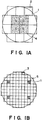
- Figures 1A and 1B are plan views, respectively, showing examples of layout of shots to be exposed by a stepper in accordance with an embodiment of the present invention.
- Figure 2 is a flow chart for explaining the operation where the layout such as shown in Figure 1A or 1B is used.
- Figure 3 is a schematic view of a projection exposure apparatus for manufacture of semiconductor devices, to which the present invention is applied.
- denoted at 100 is an illumination optical system for producing exposure light with which a pattern (having plural chip patterns) formed on a reticle 101 is projected and printed on a photosensitive resist layer, provided on a wafer 1.
- Denoted at 102 is a reticle stage for holding the reticle 101.
- the pattern of the reticle 101 is projected by a reduction projection lens 103 on the wafer, held by a wafer chuck 106, in a reduced scale.
- Denoted at 104 is an autofocus detector of known type. It projects a light beam onto the surface of the wafer 1 and, by detecting reflected light therefrom, it detects the position of the wafer surface in the direction of an optical axis (Z axis direction), with respect to the focusing plane of the projection optical system. On the basis of the result of this detection, the wafer chuck 106 is moved by a driving mechanism (not shown) in the optical axis direction of the projection lens 103, so as to place the wafer 1 surface on the focusing plane of the projection lens 103.
- Denoted at 107 is a wafer stage for moving the wafer 1, held by the wafer chuck 106, along a plane (X-Y plane) perpendicular to the optical axis of the projection lens 103. This stage performs step-and-repeat motion for sequential exposures of zones on the wafer 1.
- Denoted at 108 is a mirror which is movable integrally with the wafer stage 107 and along the X-Y plane.
- Denoted at 109 is a known laser interferometer type measuring device for measuring a position along the X-Y plane, and denoted at 110 is a console unit for controlling the projection exposure apparatus as a whole.
- Denoted at 111 is a known alignment detector for detecting an alignment mark, provided on the wafer 1, through the projection lens 103 to detect the position of the wafer 1 along the X-Y plane.
- the console unit 110 controls the projection exposure apparatus as a whole, and on the other hand it serves to make determination and selection of shot layout, to be described later. Operational steps to be described below are executed in a CPU of the console unit 110, except mentioned otherwise.
- Figures 1A and 1B are plan views showing examples of layout of shots to be exposed by a stepper according to an embodiment of the present invention.
- Figure 1A shows an exposure layout to be used in a stepper of large exposure field size in a single exposure (large picture size stepper)
- Figure 1B shows an exposure layout to be used in a stepper of small exposure field size in a single exposure (small picture size stepper) or a layout of IC or LSI chips of a number of 11.
- Denoted in these drawings at 1 is a wafer
- denoted at 2 are shots to be used in the large exposure field size stepper.
- Denoted at 4 are sample shots for alignment or global leveling, to be used in the large picture size stepper.
- Denoted at 3 are shots or IC or LSI chips to be used in the small picture size stepper.
- Denoted at 5 are sample shots for alignment or global leveling, to be used in the small picture size stepper or in the layout of IC or LSI chips.
- Figure 1A relates to an example of layout in a large picture size stepper. If in this example the exposure size is 50 mm square and the wafer 1 has a size of 8 inch diameter, then fourteen shots are defined such as shown in Figure 1A.
- a measured value related to an outside peripheral shot of the wafer contains an error due to a large variation in film thickness of a photosensitive material on the wafer or to a large distortion of the wafer 1. Excluding such outside peripheral shots of the wafer from selection of sample shots for this reason, only selectable are four sample shots 4 at the central portion of the wafer 1 as shown in Figure 1A.
- each shot 3 of the layout for the small picture size stepper shown in Figure 1B is provided with a mark (not shown) to be used for the global alignment operation, for example.
- Using these marks also in the large picture size stepper substantially makes it possible to select the sample shots 5 in the layout to be used in the small picture size stepper. This can be easily done by setting the same magnification or detecting process to the mark detecting system 111 ( Figure 3).
- a layout for a small picture size stepper or a layout of chips such as shown in Figure 1B, or alternatively a layout of mark placement on a wafer prepared separately may be used for the measurement in relation to global alignment, global leveling or die-by-die leveling, for example.
- the results of measurement may be corrected for the exposure layout of Figure 1A, and the exposure process may be performed by using corrected values and in accordance with the exposure layout. This enables high precision alignment and focus leveling even in a large picture size stepper.
- FIG 2 is a flow chart for explaining this procedure.
- a stepper after setting a reticle to be used and setting exposure conditions such as focus, exposure amount and layout preparation, actual exposure sequence starts (Step 10).
- a wafer is loaded and prealignment of the wafer is performed, and thereafter it is placed on the wafer chuck 106 ( Figure 3) of the stepper (Step 11).
- measurement positions i.e. sample shots 5 are determined in accordance with the focus leveling layout (e.g. shot layout of Figure 1B).
- the focus leveling layout e.g. shot layout of Figure 1B.
- the autofocus detector 104 Figure 3
- data measurement for the focus leveling is performed.
- the leveling is executed (Step 12).
- measurement positions (sample shots 5) are determined in accordance with the alignment layout (e.g. shot layout of Figure 1B).
- the alignment layout e.g. shot layout of Figure 1B.
- data measurement for execution of global alignment is performed (Step 13).
- calculations in relation to the shot interval and the number of shots are made to transform the measured data into exposure layout (e.g. shot layout of Figure 1A), and the placements of shots in the exposure layout are determined (Step 14). Namely, alignment data is corrected into exposure layout data.
- exposure process is performed in accordance with the thus determined placements (Step 15).
- Step 16 discrimination is made as to whether data measurement for focus and leveling to a shot to be exposed is possible or not, that is, as to whether that shot is an outside peripheral shot to which measurement is unattainable or not. If measurement is possible, drive for focus and leveling is done in accordance with a measured value (Step 17), and exposure of that shot is performed (Step 20). If that shot is one to which measurement is unattainable, the focus leveling layout is referred to and a substitute shot in the focus leveling layout adjacent to that shot is selected. Measurement for focus and leveling is done with respect to the selected substitute shot (Step 18). In accordance with the thus measured data, a value for the focus and leveling to the shot just going to be exposed with the exposure layout, is determined.
- a focus value may be determined by extrapolation to the leveling data in accordance with tilt of it.
- the leveling value may be used as it is.
- drive for focus leveling is done (Step 19).
- exposure process is performed (Step 20).
- Steps 16 - 20 are repeated with respect to every shot of the wafer. After this is completed, the wafer is unloaded (Step 22). Also, the sequential operations at Steps 11 - 22 are repeated to every wafer, and the procedure is completed (Step 24).
- Steps 11 and 12 may be inserted between Steps 14 and 15.
- the present invention is not limited to the form depicted in this flow chart.
- a separate layout or layouts other than an exposure layout may be prepared as required (for example, an exposure layout, an alignment layout and a focus leveling layout may be prepared). These different layouts may be used in the exposure of a wafer effectively.
- the alignment layout and the focus levelling layout are the same. However, they may be different from each other.
- an alignment operation may be carried out in advance of a step and repeat exposure operation, using a number of sample shot areas, to determine the alignment between the exposure pattern, typically on a reticle, and the surface to be exposed, and the correct relative positions of the exposure pattern and the surface for the exposure shot areas of the step and repeat exposure operation are calculated from the result of the alignment operation even in respect of exposure shot areas which are not used as sample shot areas in the alignment operation.
- this will involve the use of alignment marks at the sample shot areas on the surface of the exposed, and in some methods alignment marks in the exposure pattern or on the reticle may be used.
- focusing and levelling operations may be carried out using a plurality of sample shot areas and the results are used for maintaining correct focusing and levelling during the exposure operation even in respect of exposure shot areas which are not used as sample shot areas in the focusing and levelling operations.
- At least one of: an alignment operation; a focusing operation; and a levelling operation is carried out using "nominal” or “theoretical” shot areas, selected from a shot area layout which is not the same as the shot area layout used in the corresponding exposure operation.
- the "nominal" shot areas are not used as exposure shot areas in the exposure operation.
- the "nominal” shot areas are preferably smaller than the exposure shot areas.
- a “nominal” shot area may form a part of an exposure shot area, but different "nominal” shot areas are not all at the same position in the respective exposure shot areas. In this way, the spacings between "nominal" shot areas, and the positions thereof, are not constrained to be the same as for the exposure shot areas.
- the "nominal" shot areas for one exposure pattern or operation may be the exposure shot areas for a different exposure pattern or operation.
- the "nominal" shot areas may for example each be the area of one respective IC in the case that the actual exposure shot areas each cover a plurality of ICs.
- the invention can be defined in terms of shot positions, where each shot position is the relative position of the exposure pattern and the surface to be exposed.
- at least one of: an alignment operation; a levelling operation; and a focusing operation is carried out using "nominal” or “theoretical” shot positions which are not used as exposure shot positions.
- the distances between adjacent "nominal" shot positions is not an integer multiple of the distance between adjacent exposure shot positions.
- the distances between adjacent "nominal" shot positions may be an integer multiple of the distance between exposure shot positions for a different exposure operation, e.g. using a different exposure pattern.
- the surface to be exposed is the surface of a semiconductor wafer
- the distances between adjacent "nominal" shot positions may be an integer multiple of the pitch of ICs being formed on the semiconductor wafer.
- the present invention extends to methods of making exposed semiconductor wafers and methods of making integrated circuits using the present exposure method.
Landscapes
- Physics & Mathematics (AREA)
- General Physics & Mathematics (AREA)
- Exposure And Positioning Against Photoresist Photosensitive Materials (AREA)
- Exposure Of Semiconductors, Excluding Electron Or Ion Beam Exposure (AREA)
Priority Applications (1)
| Application Number | Priority Date | Filing Date | Title |
|---|---|---|---|
| EP02075268A EP1205807B1 (de) | 1994-09-05 | 1995-09-05 | Belichtungsapparat und Belichtungsverfahren |
Applications Claiming Priority (3)
| Application Number | Priority Date | Filing Date | Title |
|---|---|---|---|
| JP06234479A JP3100842B2 (ja) | 1994-09-05 | 1994-09-05 | 半導体露光装置及び露光方法 |
| JP234479/94 | 1994-09-05 | ||
| JP23447994 | 1994-09-05 |
Related Child Applications (1)
| Application Number | Title | Priority Date | Filing Date |
|---|---|---|---|
| EP02075268A Division EP1205807B1 (de) | 1994-09-05 | 1995-09-05 | Belichtungsapparat und Belichtungsverfahren |
Publications (2)
| Publication Number | Publication Date |
|---|---|
| EP0702272A1 true EP0702272A1 (de) | 1996-03-20 |
| EP0702272B1 EP0702272B1 (de) | 2002-08-07 |
Family
ID=16971668
Family Applications (2)
| Application Number | Title | Priority Date | Filing Date |
|---|---|---|---|
| EP95306182A Expired - Lifetime EP0702272B1 (de) | 1994-09-05 | 1995-09-05 | Belichtungsapparat und Belichtungsverfahren |
| EP02075268A Expired - Lifetime EP1205807B1 (de) | 1994-09-05 | 1995-09-05 | Belichtungsapparat und Belichtungsverfahren |
Family Applications After (1)
| Application Number | Title | Priority Date | Filing Date |
|---|---|---|---|
| EP02075268A Expired - Lifetime EP1205807B1 (de) | 1994-09-05 | 1995-09-05 | Belichtungsapparat und Belichtungsverfahren |
Country Status (5)
| Country | Link |
|---|---|
| US (1) | US5734462A (de) |
| EP (2) | EP0702272B1 (de) |
| JP (1) | JP3100842B2 (de) |
| KR (1) | KR0171453B1 (de) |
| DE (2) | DE69527682T2 (de) |
Cited By (3)
| Publication number | Priority date | Publication date | Assignee | Title |
|---|---|---|---|---|
| EP0807854A1 (de) * | 1996-05-15 | 1997-11-19 | Nikon Corporation | Belichtungsverfahren und -apparat |
| EP0867771A2 (de) * | 1997-03-24 | 1998-09-30 | Nikon Corporation | Belichtungsapparat, Belichtungsverfahren und Verfahren zur Herstellung einer Schaltung |
| US6455214B1 (en) | 1997-03-24 | 2002-09-24 | Nikon Corporation | Scanning exposure method detecting focus during relative movement between energy beam and substrate |
Families Citing this family (11)
| Publication number | Priority date | Publication date | Assignee | Title |
|---|---|---|---|---|
| JP3884098B2 (ja) * | 1996-03-22 | 2007-02-21 | 株式会社東芝 | 露光装置および露光方法 |
| JPH09320945A (ja) | 1996-05-24 | 1997-12-12 | Nikon Corp | 露光条件測定方法及び露光装置 |
| US5917580A (en) * | 1996-08-29 | 1999-06-29 | Canon Kabushiki Kaisha | Scan exposure method and apparatus |
| US6377337B1 (en) * | 1998-05-02 | 2002-04-23 | Canon Kabushiki Kaisha | Projection exposure apparatus |
| JP2000082651A (ja) | 1998-09-04 | 2000-03-21 | Nec Corp | 走査露光装置及び走査露光方法 |
| JP4434372B2 (ja) * | 1999-09-09 | 2010-03-17 | キヤノン株式会社 | 投影露光装置およびデバイス製造方法 |
| US6704094B2 (en) * | 2001-12-11 | 2004-03-09 | Taiwan Semiconductor Manufacturing Co., Ltd | Correction of leveling tilt induced by asymmetrical semiconductor patterns |
| US7274029B2 (en) * | 2004-12-28 | 2007-09-25 | Asml Netherlands B.V. | Lithographic apparatus and device manufacturing method |
| KR101986161B1 (ko) * | 2014-03-04 | 2019-06-05 | 에이에스엠엘 네델란즈 비.브이. | 데이터 처리 장치를 갖는 리소그래피 장치 |
| JP6397265B2 (ja) * | 2014-08-20 | 2018-09-26 | キヤノン株式会社 | リソグラフィ装置、物品の製造方法、情報処理装置及び決定方法 |
| TWI731961B (zh) | 2016-04-19 | 2021-07-01 | 德商馬克專利公司 | 正向感光材料及形成正向凸紋影像之方法 |
Citations (2)
| Publication number | Priority date | Publication date | Assignee | Title |
|---|---|---|---|---|
| EP0150129A2 (de) * | 1984-01-24 | 1985-07-31 | Hewlett-Packard Company | Verfahren und Vorrichtung für die repetitive und rotative lithographische Behandlung |
| US4780617A (en) * | 1984-08-09 | 1988-10-25 | Nippon Kogaku K.K. | Method for successive alignment of chip patterns on a substrate |
Family Cites Families (6)
| Publication number | Priority date | Publication date | Assignee | Title |
|---|---|---|---|---|
| US4734746A (en) * | 1985-06-24 | 1988-03-29 | Nippon Kogaku K. K. | Exposure method and system for photolithography |
| US4881100A (en) * | 1985-12-10 | 1989-11-14 | Canon Kabushiki Kaisha | Alignment method |
| EP0440470B1 (de) * | 1990-02-02 | 1996-12-18 | Canon Kabushiki Kaisha | Belichtungsverfahren |
| US5561606A (en) * | 1991-08-30 | 1996-10-01 | Nikon Corporation | Method for aligning shot areas on a substrate |
| JP3374413B2 (ja) * | 1992-07-20 | 2003-02-04 | 株式会社ニコン | 投影露光装置、投影露光方法、並びに集積回路製造方法 |
| JP3336649B2 (ja) * | 1992-12-25 | 2002-10-21 | 株式会社ニコン | 露光装置、露光方法、及びその露光方法を含むデバイス製造方法、及びそのデバイス製造方法により製造されたデバイス |
-
1994
- 1994-09-05 JP JP06234479A patent/JP3100842B2/ja not_active Expired - Fee Related
-
1995
- 1995-08-30 US US08/521,442 patent/US5734462A/en not_active Expired - Lifetime
- 1995-09-02 KR KR1019950028670A patent/KR0171453B1/ko not_active IP Right Cessation
- 1995-09-05 DE DE69527682T patent/DE69527682T2/de not_active Expired - Lifetime
- 1995-09-05 DE DE69536034T patent/DE69536034D1/de not_active Expired - Lifetime
- 1995-09-05 EP EP95306182A patent/EP0702272B1/de not_active Expired - Lifetime
- 1995-09-05 EP EP02075268A patent/EP1205807B1/de not_active Expired - Lifetime
Patent Citations (2)
| Publication number | Priority date | Publication date | Assignee | Title |
|---|---|---|---|---|
| EP0150129A2 (de) * | 1984-01-24 | 1985-07-31 | Hewlett-Packard Company | Verfahren und Vorrichtung für die repetitive und rotative lithographische Behandlung |
| US4780617A (en) * | 1984-08-09 | 1988-10-25 | Nippon Kogaku K.K. | Method for successive alignment of chip patterns on a substrate |
Cited By (4)
| Publication number | Priority date | Publication date | Assignee | Title |
|---|---|---|---|---|
| EP0807854A1 (de) * | 1996-05-15 | 1997-11-19 | Nikon Corporation | Belichtungsverfahren und -apparat |
| EP0867771A2 (de) * | 1997-03-24 | 1998-09-30 | Nikon Corporation | Belichtungsapparat, Belichtungsverfahren und Verfahren zur Herstellung einer Schaltung |
| EP0867771A3 (de) * | 1997-03-24 | 2000-10-25 | Nikon Corporation | Belichtungsapparat, Belichtungsverfahren und Verfahren zur Herstellung einer Schaltung |
| US6455214B1 (en) | 1997-03-24 | 2002-09-24 | Nikon Corporation | Scanning exposure method detecting focus during relative movement between energy beam and substrate |
Also Published As
| Publication number | Publication date |
|---|---|
| DE69527682T2 (de) | 2003-04-03 |
| DE69527682D1 (de) | 2002-09-12 |
| JP3100842B2 (ja) | 2000-10-23 |
| KR0171453B1 (ko) | 1999-03-20 |
| EP0702272B1 (de) | 2002-08-07 |
| US5734462A (en) | 1998-03-31 |
| JPH0878317A (ja) | 1996-03-22 |
| EP1205807A1 (de) | 2002-05-15 |
| DE69536034D1 (de) | 2010-02-04 |
| EP1205807B1 (de) | 2009-12-23 |
| KR960011565A (ko) | 1996-04-20 |
Similar Documents
| Publication | Publication Date | Title |
|---|---|---|
| US6481003B1 (en) | Alignment method and method for producing device using the alignment method | |
| JP3402750B2 (ja) | 位置合わせ方法及びそれを用いた素子の製造方法 | |
| US5403754A (en) | Lithography method for direct alignment of integrated circuits multiple layers | |
| JP4434372B2 (ja) | 投影露光装置およびデバイス製造方法 | |
| EP1205807B1 (de) | Belichtungsapparat und Belichtungsverfahren | |
| US20020037460A1 (en) | Stage unit, measurement unit and measurement method, and exposure apparatus and exposure method | |
| US9046788B2 (en) | Method for monitoring focus on an integrated wafer | |
| JP3809268B2 (ja) | デバイス製造方法 | |
| US8384900B2 (en) | Exposure apparatus | |
| US20060033916A1 (en) | Selection method, exposure method, selection unit, exposure apparatus, and device manufacturing method | |
| JP2005012021A (ja) | 露光装置、及び当該装置を用いたデバイス製造方法、位置合わせ方法、並びにステージ装置 | |
| JPH09199406A (ja) | 位置検出装置及びそれを用いた半導体素子の製造方法 | |
| US20030020889A1 (en) | Stage unit, measurement unit and measurement method, and exposure apparatus and exposure method | |
| EP1372041A2 (de) | Steuerung eines Gerätes zur Belichtung einer Halbleitervorrichtung | |
| JP2009200122A (ja) | 露光装置およびデバイス製造方法 | |
| US6569579B2 (en) | Semiconductor mask alignment system utilizing pellicle with zero layer image placement indicator | |
| JP5084432B2 (ja) | 露光方法、露光装置およびデバイス製造方法 | |
| US7852458B2 (en) | Exposure apparatus | |
| US20030003384A1 (en) | Aligning method, exposure method, exposure apparatus, and device manufacturing method | |
| JP3651630B2 (ja) | 投影露光方法及び投影露光装置 | |
| US6559927B1 (en) | Gap adjusting method in exposure apparatus | |
| JP2006148013A (ja) | 位置合わせ方法及び露光方法 | |
| KR100889843B1 (ko) | 주사형 노광장치 및 디바이스 제조방법 | |
| US4881100A (en) | Alignment method | |
| US20100309486A1 (en) | Pattern transfer apparatus and method of manufacturing device |
Legal Events
| Date | Code | Title | Description |
|---|---|---|---|
| PUAI | Public reference made under article 153(3) epc to a published international application that has entered the european phase |
Free format text: ORIGINAL CODE: 0009012 |
|
| AK | Designated contracting states |
Kind code of ref document: A1 Designated state(s): DE GB NL |
|
| 17P | Request for examination filed |
Effective date: 19960801 |
|
| 17Q | First examination report despatched |
Effective date: 19980421 |
|
| GRAG | Despatch of communication of intention to grant |
Free format text: ORIGINAL CODE: EPIDOS AGRA |
|
| GRAG | Despatch of communication of intention to grant |
Free format text: ORIGINAL CODE: EPIDOS AGRA |
|
| GRAH | Despatch of communication of intention to grant a patent |
Free format text: ORIGINAL CODE: EPIDOS IGRA |
|
| GRAH | Despatch of communication of intention to grant a patent |
Free format text: ORIGINAL CODE: EPIDOS IGRA |
|
| GRAA | (expected) grant |
Free format text: ORIGINAL CODE: 0009210 |
|
| AK | Designated contracting states |
Kind code of ref document: B1 Designated state(s): DE GB NL |
|
| REG | Reference to a national code |
Ref country code: GB Ref legal event code: FG4D |
|
| REF | Corresponds to: |
Ref document number: 69527682 Country of ref document: DE Date of ref document: 20020912 |
|
| PLBE | No opposition filed within time limit |
Free format text: ORIGINAL CODE: 0009261 |
|
| STAA | Information on the status of an ep patent application or granted ep patent |
Free format text: STATUS: NO OPPOSITION FILED WITHIN TIME LIMIT |
|
| 26N | No opposition filed |
Effective date: 20030508 |
|
| PGFP | Annual fee paid to national office [announced via postgrant information from national office to epo] |
Ref country code: GB Payment date: 20080911 Year of fee payment: 14 |
|
| GBPC | Gb: european patent ceased through non-payment of renewal fee |
Effective date: 20090905 |
|
| PG25 | Lapsed in a contracting state [announced via postgrant information from national office to epo] |
Ref country code: GB Free format text: LAPSE BECAUSE OF NON-PAYMENT OF DUE FEES Effective date: 20090905 |
|
| PGFP | Annual fee paid to national office [announced via postgrant information from national office to epo] |
Ref country code: DE Payment date: 20130930 Year of fee payment: 19 Ref country code: NL Payment date: 20130916 Year of fee payment: 19 |
|
| REG | Reference to a national code |
Ref country code: DE Ref legal event code: R119 Ref document number: 69527682 Country of ref document: DE |
|
| PG25 | Lapsed in a contracting state [announced via postgrant information from national office to epo] |
Ref country code: NL Free format text: LAPSE BECAUSE OF NON-PAYMENT OF DUE FEES Effective date: 20150401 |
|
| PG25 | Lapsed in a contracting state [announced via postgrant information from national office to epo] |
Ref country code: DE Free format text: LAPSE BECAUSE OF NON-PAYMENT OF DUE FEES Effective date: 20150401 |