EP0683520B1 - Verfahren zur Herstellung einer Anordnung zur Kontaktierung von planaren Hochfrequenzleitungen und Anordnung zur Kontaktierung von planaren Hochfrequenzleitungen - Google Patents
Verfahren zur Herstellung einer Anordnung zur Kontaktierung von planaren Hochfrequenzleitungen und Anordnung zur Kontaktierung von planaren Hochfrequenzleitungen Download PDFInfo
- Publication number
- EP0683520B1 EP0683520B1 EP95106296A EP95106296A EP0683520B1 EP 0683520 B1 EP0683520 B1 EP 0683520B1 EP 95106296 A EP95106296 A EP 95106296A EP 95106296 A EP95106296 A EP 95106296A EP 0683520 B1 EP0683520 B1 EP 0683520B1
- Authority
- EP
- European Patent Office
- Prior art keywords
- layer
- over
- substrate
- metal layer
- depression
- Prior art date
- Legal status (The legal status is an assumption and is not a legal conclusion. Google has not performed a legal analysis and makes no representation as to the accuracy of the status listed.)
- Expired - Lifetime
Links
Images


Classifications
-
- H—ELECTRICITY
- H10—SEMICONDUCTOR DEVICES; ELECTRIC SOLID-STATE DEVICES NOT OTHERWISE PROVIDED FOR
- H10W—GENERIC PACKAGES, INTERCONNECTIONS, CONNECTORS OR OTHER CONSTRUCTIONAL DETAILS OF DEVICES COVERED BY CLASS H10
- H10W44/00—Electrical arrangements for controlling or matching impedance
- H10W44/20—Electrical arrangements for controlling or matching impedance at high-frequency [HF] or radio frequency [RF]
Definitions
- the invention relates to a method for producing a Arrangement for contacting planar Radio frequency lines with electronic components, as well an arrangement for contacting planar Radio frequency lines with electronic components.
- a disadvantage of these adapter substrates according to the prior art Technique is that it is very difficult to get the metal strips in the required small size on the lines of the Attach adapter substrates.
- the maximum size of the Metal strip is due to the contact gap on the Microchip and by the maximum, with the metal strips bridgeable length specified.
- a circuit arrangement is in EP-A1-0 001 707 described in the case of a window of a silicon plate Circuit arrangements thermally insulated via stirrups are hung on silicon wafers.
- the bridges exist from a protective layer, an adhesive layer with the Properties of an electrical resistance or one Layer of chrome or titanium and a metal layer, for example made of stainless steel. This electric conductive bridges provide thermal insulation between the silicon frame of the window and the ones arranged in it Silicon wafers.
- U.S. Patent 3,747,202 is concerned with one Improvement of the newly developed beam lead procedure. This procedure will be on the surface of semiconductor devices thick conductor structures not applied over the edge area of the protrude isolated component.
- the wafer becomes semiconductor components from below in one wide separation area etched away, so that over the chip edge protruding conductor tracks (English Beam Leads) stay.
- the chips with the protruding conductor tracks are flipped over accordingly structured conductor tracks of a substrate applied and in a beam lead bonder or by a soldering process firmly connected together with the substrate conductor tracks. there the separation of the beam leads from the wafer surface by undercutting away an adhesive layer below the parts of the Beam leads reached.
- connection tongues built up from a component carrier. These tongues come with corresponding contact surfaces firmly connected to the components.
- the connecting tongues consist of a resin film with an underlying one Attachment layer and an overlying structured wiring layer. This Wiring layer contacts the connection pads Components through holes in the hard film, the Embankment wheels are inclined to tear off the Avoid wiring layer.
- connection structures In both documents there are fixed links from there described connection structures to the connection areas describe the components. These connection structures should be permanent electrical and Establish mechanical connection with a carrier substrate. There is only one conductor for each electrical channel provided what for DC voltage contact or for Connections in the low and medium frequency range is sufficient.
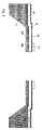
- Figure 1 shows a substrate 1, here for example Silicon, in cross section.
- the silicon substrate is applied its top 2 and on its bottom 3 each Passivation layer 4 or 5, for example each of a double layer of silicon oxide and silicon nitride consist.
- the lower passivation layer photolithographically opened a window 6 through which the Well 7 is anisotropically etched.
- the Crystal orientation of the silicon substrate 1 selected that the (100) plane is parallel to the substrate surface.
- the edges of the rectangular window 6 lie here parallel to the crystallographic [110] directions.
- the Well 7 is etched until the Passivation layer 4 reached on the top of the substrate is.
- the side walls of the recess 7 are heavy etchable ⁇ 111 ⁇ planes.
- a metal layer 8 On top of the substrate is over the Passivation layer 4 a metal layer 8, a Dielectric layer 9 and a further metal layer 10 upset.
- the metal layers 8 and 10 can preferably made of gold and the dielectric layer 9 Polyimide exist.
- the lower metal layer 8 is except for the vicinity of the upper surface 12 of the recess 7 unstructured and serves as a ground plane. Within the Window surface 12, the metal layer 8 except for the Conductor structures such as those in the upper metal layer 10 are provided, etched away.
- the top metal layer 10 will photolithographically to produce the microstrips or Structured coplanar lines. In the area of deepening conductor ends or spanning conductors are provided. These can be at the designated contact points Contact improvement metallic bumps or pads (11).
- Figure 2 shows a plan view of the top of the Substrate, with the waveguides as coplanar lines with the hot line 100 and the side ground lines 101 are designed.
- Figure 3 is a plan view of a substrate with Microstrip waveguides shown.
- the substrate 1 with the layers thereon is after structuring along the cut surface Sawed A-A 'and in a production with multiple uses isolated.
- Such Arrangement is shown in Figure 4 in the application.
- the Arrangement is overhead and slightly tilted over one Microchip 50 held and contacted there with the Contact bump 11 the contact 51 of the microchip.
- the conductor structures are on the Metal layer 8 and the metal layer 10 when considering the underside of the substrate at the top see the transparent layers 4 and 9 through. This makes an optical adjustment of the conductor structures the contacts on the microchip possible. Besides, it is advantageous over the prior art that the etched side surfaces of the recess 7 extend inclined. When considering the contact geometry with a Microscope objective with a high aperture will imaging light beams not trimmed.
- Another embodiment of the arrangement according to the invention can consist in that not only the metal layers 8 and 10, but also the passivation layer 4 and the dielectric layer 9 are structured.
- the micromechanical structuring from the substrate underside can take place before the coating and structuring of the layers 8 to 11 on the substrate top. Since the passivation layer 4 is retained in KOH on the upper side of the substrate after the anisotropic etching has been carried out, a flat surface remains on the upper side, on which the layers 4 to 11 can be built and structured. This order of processing prevents layers 4 to 11 from being attacked by the etchant for the anisotropic etching. There are 7 self-supporting tongues, each with at least one conductor end, above the recess.
- layers 4, 8 and 9 must be adapted to that of the upper metal layer, but the structures can be significantly larger or wider. It is possible to build up mechanical stresses in the layer sequences 4, 8, 9 and 10 in such a way that the tongues protruding beyond the recess 7 bend upwards. This achieves a greater height of the contact pads 11 above the substrate surface and, at the same time, a greater spring action of the contacts.
- a larger height of the contacts 11 above the wafer surface can also be achieved in that the polyimide 9 in Contact area receives a thickening 81, as in Figure 5 is shown.
- the probe according to the invention also be designed so that not only Connections on one side of the chip are possible, but that all 4 chip sides are contacted at the same time can. An exemplary embodiment of this is shown in FIG. 6 shown.
- FIG. 7 Another embodiment of the invention is shown in FIG. 7 shown.
- the recess 7 is initially not whole, but only up to an etch stop layer near the top etched through.
- Such an etch stop layer can be after State of the art by increased boron doping or by a diffused pn junction.
- the anisotropic etching stops automatically at the etching stop layer, so that when etching from the bottom on the top a thin membrane 20 remains.
- This membrane can now by isotropic or anisotropic etching from the top to be structured into tongues that the line transitions in Wear contact area.
- the tongues can be removed by putting on a Bend the control voltage upwards. In this way it is possible to have individual or all contacts of a microchip optionally to contact.
Landscapes
- Waveguides (AREA)
- Measuring Leads Or Probes (AREA)
- Internal Circuitry In Semiconductor Integrated Circuit Devices (AREA)
Description
Es entstehen über der Vertiefung 7 freitragende Zungen mit je mindestens einem Leiterende. Die Strukturierung der Schichten 4, 8 und 9 muß wohl an die der oberen Metallschicht angepaßt sein, die Strukturen können aber wesentlich größer oder breiter sein.
Es ist möglich in den Schichtenfolgen 4, 8, 9 und 10 gezielt mechanische Spannungen in der Art aufzubauen, daß sich die über die Vertiefung 7 hinausragenden Zungen nach oben biegen. Dadurch wird eine größere Höhe der Kontaktflecken 11 über der Substratoberfläche und zugleich eine größere Federwirkung der Kontakte erreicht.
Claims (9)
- Verfahren zur Herstellung einer Anordnung zur Kontaktierung von planaren Hochfrequenzleitungen mit elektronischen Bauelementen mit folgenden Verfahrensschritten:a) auf die Oberseite (2) und die Unterseite (3) eines Substrates (1) wird je eine Passivierungsschicht (4, 5) aufgebracht;b) in der unteren Passivierungsschicht (5) wird ein Fenster (6) geöffnet und eine Vertiefung (7) von der Unterseite (3) ins Substrat (1) geätzt, die bis zur Passivierungsschicht (4) auf der Oberseite (2) oder bis zu einer Ätzstopschicht (20) an der Oberseite (2) reicht;c) auf der Oberseite (2) werden über die Passivierungsschicht (4) eine untere Metallschicht (8), darüber eine Dielektrikumschicht (9) und darüber eine weitere obere Metallschicht (10) aufgebracht;d) die obere Metallschicht (10) wird zur Erzeugung von planaren Leitermustern strukturiert, wobei im Bereich der Vertiefung (7) zumindest ein Leiter vorgesehen ist, der über der Vertiefung endet oder diese überspannt;e) die untere Metallschicht (8) wird vor dem Aufbringen der Dielektrikumschicht (9) im Bereich der Vertiefung (7) ebenso wie die obere Metallschicht (10) strukturiert;f) das Substrat wird derart zersägt und/oder bei einer Fertigung mit Mehrfachnutzen vereinzelt, daß über der Vertiefung freitragende Zungen mit jeweils zumindest einem Leiterende entstehen.
- Verfahren zur Herstellung einer Anordnung zur Kontaktierung von planaren Hochfrequenzleitungen mit elektronischen Bauelementen mit folgenden Verfahrensschritten:a) auf die Oberseite (2) und die Unterseite (3) eines Substrates (1) wird je eine Passivierungsschicht (4, 5) aufgebracht;b) in der unteren Passivierungsschicht (5) wird ein Fenster (6) geöffnet und eine Vertiefung (7) von der Unterseite (3) ins Substrat (1) geätzt, die bis zur Passivierungsschicht (4) auf der Oberseite (2) oder bis zu einer Ätzstopschicht (20) nahe der Oberseite (2) reicht;c) auf der Oberseite (2) werden über die Passivierungsschicht (4) eine untere Metallschicht (8), darüber eine Dielektrikumschicht (9) und darüber eine weitere obere Metallschicht (10) aufgebracht;d) die obere Metallschicht (10) wird zur Erzeugung von planaren Leitermustern strukturiert, wobei im Bereich der Vertiefung (7) zumindest ein Leiter vorgesehen ist, der über der Vertiefung endet;e) die untere Metallschicht (8) wird im Bereich der Vertiefung (7) ebenso wie die obere Metallschicht (10) struktuiert;f) die Dielektrikumschicht (9) und die Passivierungsschicht (4) oder die Dielektrikumsschicht (9), die Passivierungsschicht (4) und eine noch verbleibende dünne Substratschicht über der Ätzstopschicht (20) werden im Bereich der Vertiefung (7) durch Ätzen derart strukturiert, daß die Leiterenden über der Vertiefung (7) aus freitragenden Zungen zumindest mit untere Metallschicht (8), Dielektrikumschicht (9) und Obere Metallschicht (10) bestehen.
- Passivierungsschicht (4), untere Metallschicht (8),
Dielektrikumsschicht (9) und obere Metallschicht (10) mechanische Spannungen derart aufgebaut werden, daß sich die Zungen vom Substrat weg biegen. - Verfahren nach einem der Ansprüche 1 bis 3, dadurch gekennzeichnet, daß an den über der Vertiefung befindlichen Enden der Leiterbahnen eine Verdickung auf der Dielektrikumsschicht (9) aufgebracht wird.
- Anordnung zur Kontaktierung von planaren
Hochfrequenzleitungen mit elektronischen Bauelementen mit folgenden Merkmalen:a) ein Substrat (1) trägt auf seiner Oberseite (2) eine Passivierungsschicht (4), darüber eine untere Metallschicht (8), darüber eine Dielektriumschicht (9) und darüber eine weitere Obere Metallschicht (10), die entsprechend einem vorgegebenen Leitermuster strukturiert ist;b) im Substrat (1) befindet sich eine Vertiefung (7), die von der Unterseite (3) bis zur Passivierungssschicht (4) auf der Oberseite (2) oder bis zu einer Ätzstopschicht (20) an der Oberseite (2) des Substrats (1) reicht;c) im Bereich der Vertiefung (7) ist zumindest ein Leiter vorgesehen, der über der Vertiefung (7) endet;d) die untere Metallschicht (8) ist im Bereich der Vertiefung (7) ebenso wie die obere Metallschicht (10) strukturiert. - Anordnung zur Kontaktierung von planaren
Hochfrequenzleitungen mit elektronischen Bauelementen mit folgenden Merkmalen:a) ein Substrat (1) trägt auf seiner Oberseite (2) eine Passivierungsschicht (4), darüber eine untere Metallschicht (8), darüber eine Dielektriumschicht (9) und darüber eine weitere Obere Metallschicht (10), die entsprechend einem vorgegebenen Leitermuster strukturiert ist;b) an einem Rand des Substrats (1) befindet sich ein abgesetzter Bereich (7), der von der Unterseite (3) bis zur Passivierungssschicht (4) auf der Oberseite (2) oder bis zu einer Ätzstopschicht (20) an der Oberseite (2) des Substrats (1) reicht;c) über dem abgesetzten Bereich (7) endet zumindest ein Leiter;d) die untere Metallschicht (8) ist über dem abgesetzten Bereich (7) ebenso wie die obere Metallschicht (10) strukturiert. - Anordnung nach Anspruch 6, dadurch gekennzeichnet, daß auf den Leiterenden am Rand des Substrates (1) zusätzliche metallische Kotaktflächen (11) vorgesehen sind.
- Anordnung nach einem der Ansprüche 5 bis 8, dadurch gekennzeichnet, daß auf der Oberseite des Substrates (1) elektronische Ansteuer- (30) oder Empfängerschaltungen (3) vorgesehen sind.
- Anordnung nach einem der Ansprüche 5 bis 8, dadurch gekennzeichnet, daß sich der über die Vertiefung (7) bzw. über den abgesetzten Bereich überstehende Teil mit Leiter und Dielektrikumsschicht (9) vom Substrat (1) weg biegt.
Applications Claiming Priority (2)
| Application Number | Priority Date | Filing Date | Title |
|---|---|---|---|
| DE4416980A DE4416980C2 (de) | 1994-05-13 | 1994-05-13 | Anordnung zur Kontaktierung von planaren Hochfrequenzleitungen und Verfahren zur Herstellung einer Anordnung zur Kontaktierung von planaren Hochfrequenzleitungen |
| DE4416980 | 1994-05-13 |
Publications (3)
| Publication Number | Publication Date |
|---|---|
| EP0683520A2 EP0683520A2 (de) | 1995-11-22 |
| EP0683520A3 EP0683520A3 (de) | 1998-02-25 |
| EP0683520B1 true EP0683520B1 (de) | 2001-12-05 |
Family
ID=6518115
Family Applications (1)
| Application Number | Title | Priority Date | Filing Date |
|---|---|---|---|
| EP95106296A Expired - Lifetime EP0683520B1 (de) | 1994-05-13 | 1995-04-27 | Verfahren zur Herstellung einer Anordnung zur Kontaktierung von planaren Hochfrequenzleitungen und Anordnung zur Kontaktierung von planaren Hochfrequenzleitungen |
Country Status (2)
| Country | Link |
|---|---|
| EP (1) | EP0683520B1 (de) |
| DE (2) | DE4416980C2 (de) |
Families Citing this family (1)
| Publication number | Priority date | Publication date | Assignee | Title |
|---|---|---|---|---|
| US6953992B2 (en) | 2001-09-20 | 2005-10-11 | Infineon Technologies Ag | Electronic component with at least one semiconductor chip and method for its manufacture |
Family Cites Families (8)
| Publication number | Priority date | Publication date | Assignee | Title |
|---|---|---|---|---|
| US4189342A (en) * | 1971-10-07 | 1980-02-19 | U.S. Philips Corporation | Semiconductor device comprising projecting contact layers |
| US3747202A (en) * | 1971-11-22 | 1973-07-24 | Honeywell Inf Systems | Method of making beam leads on substrates |
| US4246595A (en) * | 1977-03-08 | 1981-01-20 | Matsushita Electric Industrial Co., Ltd. | Electronics circuit device and method of making the same |
| US4257061A (en) * | 1977-10-17 | 1981-03-17 | John Fluke Mfg. Co., Inc. | Thermally isolated monolithic semiconductor die |
| JPS58115842A (ja) * | 1981-12-28 | 1983-07-09 | Fujitsu Ltd | 半導体装置 |
| FR2565030B1 (fr) * | 1984-05-25 | 1986-08-22 | Thomson Csf | Structure de metallisations de reprise de contacts d'un dispositif semi-conducteur et dispositif dote d'une telle structure |
| US4996582A (en) * | 1988-09-14 | 1991-02-26 | Mitsubishi Denki Kabushiki Kaisha | Field effect transistor for microstrip mounting and microstrip-mounted transistor assembly |
| JP2763445B2 (ja) * | 1992-04-03 | 1998-06-11 | 三菱電機株式会社 | 高周波信号用配線及びそのボンディング装置 |
-
1994
- 1994-05-13 DE DE4416980A patent/DE4416980C2/de not_active Expired - Fee Related
-
1995
- 1995-04-27 DE DE59509894T patent/DE59509894D1/de not_active Expired - Fee Related
- 1995-04-27 EP EP95106296A patent/EP0683520B1/de not_active Expired - Lifetime
Also Published As
| Publication number | Publication date |
|---|---|
| DE4416980A1 (de) | 1995-11-23 |
| DE59509894D1 (de) | 2002-01-17 |
| EP0683520A2 (de) | 1995-11-22 |
| EP0683520A3 (de) | 1998-02-25 |
| DE4416980C2 (de) | 1998-04-09 |
Similar Documents
| Publication | Publication Date | Title |
|---|---|---|
| EP0769209B1 (de) | Verfahren zur herstellung einer dreidimensionalen schaltungsanordnung | |
| DE3888476T2 (de) | Elektrische Kontaktstellen und damit versehene Gehäuse. | |
| DE69228863T2 (de) | Selbstausrichtende optische Baugruppe und Verfahren zur Bildung derselben | |
| EP0698288B1 (de) | Herstellungsverfahren für vertikal kontaktierte halbleiterbauelemente | |
| DE69733115T2 (de) | Millimeter-Hohlleiter und Schaltungsanordnung mit diesem Hohlleiter | |
| DE69019530T2 (de) | Mikromechanischer schalter. | |
| EP0739540B1 (de) | Verfahren zur herstellung einer dreidimensionalen schaltungsanordnung | |
| DE10037216A1 (de) | Anschlußstruktur sowie Verfahren zur Herstellung von Anschlußelementen und Verfahren zur Erzeugung einer Anschlußstruktur | |
| DE10151125A1 (de) | Anschlussstruktur und zugehöriges Herstellungsverfahren sowie die Anschlussstruktur verwendende Prüfanschlussanordnung | |
| DE4318241A1 (de) | Substrat | |
| DE10392306T5 (de) | Kontaktstruktur mit Siliziumtastkontaktgeber | |
| DE69209970T2 (de) | Höckerelektrodenstruktur und Halbleiterchip mit dieser Struktur | |
| WO2003067646A2 (de) | Halbleitersubstrat mit einem elektrisch isolierten bereich, insbesondere zur vertikalintegration | |
| EP3424072B1 (de) | Verfahren zur herstellung eines halbleiterbauelements und halbleiterbauelement | |
| EP0865081B1 (de) | Verfahren zum Herstellen von elektronischen Elementen | |
| EP0463297A1 (de) | Anordnung aus Substrat und Bauelement und Verfahren zur Herstellung | |
| DE10351028B4 (de) | Halbleiter-Bauteil sowie dafür geeignetes Herstellungs-/Montageverfahren | |
| DE19719853A1 (de) | Hochfrequenz-Halbleitermodul | |
| DE10035976A1 (de) | Anschlussstruktur, Verfahren zur Herstellung einer Anschlussstruktur sowie Handhabungsmechanismus für Anschlusselemente | |
| DE3930621A1 (de) | Feldeffekt-transistor und -transistoranordnung fuer mikrostreifenleitertechnik | |
| DE102013202806B4 (de) | Schaltung auf dünnem Träger für den Einsatz in Hohlleitern und Herstellungsverfahren | |
| DE68910327T2 (de) | Halbleiteranordnung. | |
| DE4416980C2 (de) | Anordnung zur Kontaktierung von planaren Hochfrequenzleitungen und Verfahren zur Herstellung einer Anordnung zur Kontaktierung von planaren Hochfrequenzleitungen | |
| DE10393265T5 (de) | Mikrovorrichtung und Verfahren zu deren Herstellung | |
| DE3522168C2 (de) | Verfahren zum Masseverbinden von planaren Bauelementen und integrierten Schaltkreisen |
Legal Events
| Date | Code | Title | Description |
|---|---|---|---|
| PUAI | Public reference made under article 153(3) epc to a published international application that has entered the european phase |
Free format text: ORIGINAL CODE: 0009012 |
|
| AK | Designated contracting states |
Kind code of ref document: A2 Designated state(s): DE FR GB IT SE |
|
| RAP1 | Party data changed (applicant data changed or rights of an application transferred) |
Owner name: ROBERT BOSCH GMBH |
|
| PUAL | Search report despatched |
Free format text: ORIGINAL CODE: 0009013 |
|
| AK | Designated contracting states |
Kind code of ref document: A3 Designated state(s): DE FR GB IT SE |
|
| 17P | Request for examination filed |
Effective date: 19980825 |
|
| 17Q | First examination report despatched |
Effective date: 19981112 |
|
| GRAG | Despatch of communication of intention to grant |
Free format text: ORIGINAL CODE: EPIDOS AGRA |
|
| GRAG | Despatch of communication of intention to grant |
Free format text: ORIGINAL CODE: EPIDOS AGRA |
|
| GRAG | Despatch of communication of intention to grant |
Free format text: ORIGINAL CODE: EPIDOS AGRA |
|
| GRAH | Despatch of communication of intention to grant a patent |
Free format text: ORIGINAL CODE: EPIDOS IGRA |
|
| GRAH | Despatch of communication of intention to grant a patent |
Free format text: ORIGINAL CODE: EPIDOS IGRA |
|
| GRAA | (expected) grant |
Free format text: ORIGINAL CODE: 0009210 |
|
| AK | Designated contracting states |
Kind code of ref document: B1 Designated state(s): DE FR GB IT SE |
|
| REG | Reference to a national code |
Ref country code: GB Ref legal event code: IF02 |
|
| REF | Corresponds to: |
Ref document number: 59509894 Country of ref document: DE Date of ref document: 20020117 |
|
| GBT | Gb: translation of ep patent filed (gb section 77(6)(a)/1977) |
Effective date: 20020221 |
|
| ET | Fr: translation filed | ||
| PLBE | No opposition filed within time limit |
Free format text: ORIGINAL CODE: 0009261 |
|
| STAA | Information on the status of an ep patent application or granted ep patent |
Free format text: STATUS: NO OPPOSITION FILED WITHIN TIME LIMIT |
|
| 26N | No opposition filed | ||
| REG | Reference to a national code |
Ref country code: GB Ref legal event code: 732E |
|
| REG | Reference to a national code |
Ref country code: GB Ref legal event code: 732E |
|
| REG | Reference to a national code |
Ref country code: FR Ref legal event code: TP |
|
| PGFP | Annual fee paid to national office [announced via postgrant information from national office to epo] |
Ref country code: GB Payment date: 20040318 Year of fee payment: 10 |
|
| PGFP | Annual fee paid to national office [announced via postgrant information from national office to epo] |
Ref country code: SE Payment date: 20040406 Year of fee payment: 10 |
|
| PGFP | Annual fee paid to national office [announced via postgrant information from national office to epo] |
Ref country code: FR Payment date: 20040408 Year of fee payment: 10 |
|
| PGFP | Annual fee paid to national office [announced via postgrant information from national office to epo] |
Ref country code: DE Payment date: 20040506 Year of fee payment: 10 |
|
| PG25 | Lapsed in a contracting state [announced via postgrant information from national office to epo] |
Ref country code: IT Free format text: LAPSE BECAUSE OF NON-PAYMENT OF DUE FEES;WARNING: LAPSES OF ITALIAN PATENTS WITH EFFECTIVE DATE BEFORE 2007 MAY HAVE OCCURRED AT ANY TIME BEFORE 2007. THE CORRECT EFFECTIVE DATE MAY BE DIFFERENT FROM THE ONE RECORDED. Effective date: 20050427 Ref country code: GB Free format text: LAPSE BECAUSE OF NON-PAYMENT OF DUE FEES Effective date: 20050427 |
|
| PG25 | Lapsed in a contracting state [announced via postgrant information from national office to epo] |
Ref country code: SE Free format text: LAPSE BECAUSE OF NON-PAYMENT OF DUE FEES Effective date: 20050428 |
|
| PG25 | Lapsed in a contracting state [announced via postgrant information from national office to epo] |
Ref country code: DE Free format text: LAPSE BECAUSE OF NON-PAYMENT OF DUE FEES Effective date: 20051101 |
|
| EUG | Se: european patent has lapsed | ||
| GBPC | Gb: european patent ceased through non-payment of renewal fee |
Effective date: 20050427 |
|
| PG25 | Lapsed in a contracting state [announced via postgrant information from national office to epo] |
Ref country code: FR Free format text: LAPSE BECAUSE OF NON-PAYMENT OF DUE FEES Effective date: 20051230 |
|
| REG | Reference to a national code |
Ref country code: FR Ref legal event code: ST Effective date: 20051230 |