EP0680804A1 - Verfahren zur Bearbeitung von oxidischen Materialien mittels eines Laserstrahls - Google Patents
Verfahren zur Bearbeitung von oxidischen Materialien mittels eines Laserstrahls Download PDFInfo
- Publication number
- EP0680804A1 EP0680804A1 EP95610024A EP95610024A EP0680804A1 EP 0680804 A1 EP0680804 A1 EP 0680804A1 EP 95610024 A EP95610024 A EP 95610024A EP 95610024 A EP95610024 A EP 95610024A EP 0680804 A1 EP0680804 A1 EP 0680804A1
- Authority
- EP
- European Patent Office
- Prior art keywords
- band gap
- laser
- energy
- laser beam
- less
- Prior art date
- Legal status (The legal status is an assumption and is not a legal conclusion. Google has not performed a legal analysis and makes no representation as to the accuracy of the status listed.)
- Granted
Links
Images


Classifications
-
- C—CHEMISTRY; METALLURGY
- C04—CEMENTS; CONCRETE; ARTIFICIAL STONE; CERAMICS; REFRACTORIES
- C04B—LIME, MAGNESIA; SLAG; CEMENTS; COMPOSITIONS THEREOF, e.g. MORTARS, CONCRETE OR LIKE BUILDING MATERIALS; ARTIFICIAL STONE; CERAMICS; REFRACTORIES; TREATMENT OF NATURAL STONE
- C04B41/00—After-treatment of mortars, concrete, artificial stone or ceramics; Treatment of natural stone
- C04B41/009—After-treatment of mortars, concrete, artificial stone or ceramics; Treatment of natural stone characterised by the material treated
-
- B—PERFORMING OPERATIONS; TRANSPORTING
- B23—MACHINE TOOLS; METAL-WORKING NOT OTHERWISE PROVIDED FOR
- B23K—SOLDERING OR UNSOLDERING; WELDING; CLADDING OR PLATING BY SOLDERING OR WELDING; CUTTING BY APPLYING HEAT LOCALLY, e.g. FLAME CUTTING; WORKING BY LASER BEAM
- B23K26/00—Working by laser beam, e.g. welding, cutting or boring
- B23K26/36—Removing material
- B23K26/40—Removing material taking account of the properties of the material involved
-
- C—CHEMISTRY; METALLURGY
- C04—CEMENTS; CONCRETE; ARTIFICIAL STONE; CERAMICS; REFRACTORIES
- C04B—LIME, MAGNESIA; SLAG; CEMENTS; COMPOSITIONS THEREOF, e.g. MORTARS, CONCRETE OR LIKE BUILDING MATERIALS; ARTIFICIAL STONE; CERAMICS; REFRACTORIES; TREATMENT OF NATURAL STONE
- C04B41/00—After-treatment of mortars, concrete, artificial stone or ceramics; Treatment of natural stone
- C04B41/53—After-treatment of mortars, concrete, artificial stone or ceramics; Treatment of natural stone involving the removal of at least part of the materials of the treated article, e.g. etching, drying of hardened concrete
-
- C—CHEMISTRY; METALLURGY
- C04—CEMENTS; CONCRETE; ARTIFICIAL STONE; CERAMICS; REFRACTORIES
- C04B—LIME, MAGNESIA; SLAG; CEMENTS; COMPOSITIONS THEREOF, e.g. MORTARS, CONCRETE OR LIKE BUILDING MATERIALS; ARTIFICIAL STONE; CERAMICS; REFRACTORIES; TREATMENT OF NATURAL STONE
- C04B41/00—After-treatment of mortars, concrete, artificial stone or ceramics; Treatment of natural stone
- C04B41/80—After-treatment of mortars, concrete, artificial stone or ceramics; Treatment of natural stone of only ceramics
- C04B41/91—After-treatment of mortars, concrete, artificial stone or ceramics; Treatment of natural stone of only ceramics involving the removal of part of the materials of the treated articles, e.g. etching
-
- B—PERFORMING OPERATIONS; TRANSPORTING
- B23—MACHINE TOOLS; METAL-WORKING NOT OTHERWISE PROVIDED FOR
- B23K—SOLDERING OR UNSOLDERING; WELDING; CLADDING OR PLATING BY SOLDERING OR WELDING; CUTTING BY APPLYING HEAT LOCALLY, e.g. FLAME CUTTING; WORKING BY LASER BEAM
- B23K2103/00—Materials to be soldered, welded or cut
- B23K2103/50—Inorganic material, e.g. metals, not provided for in B23K2103/02 – B23K2103/26
- B23K2103/52—Ceramics
Definitions
- the invention relates to a method of processing bodies of oxide materials by means of a laser beam.
- the method is intended to be used for the provision of well-defined, three-dimensional structures in oxide materials.
- One of the materials to be processed is LiNbO3.
- Commercially available LiNbO3 is piezoelectric with a complex crystal structure, as inter alia the ratio between Li and Nb usually deviates from the stoichiometric ratio of 1:1.
- the material is an insulator having a band gap of approximately 3.7 eV at 300°K.
- the band structure is not known in details.
- the material has various possible applications, as the optical as well as the piezoelectric properties may be utilized. As it hitherto has proved extremely difficult to process said material, (i.e. to selectively remove the material from a well-defined area of a substrate surface), new methods having considerably increased removal rates may be of great importance.
- Table 1 shows the removal rates for some of the known processing methods.
- Table 1 Method Typical Rate Remarks Conventional wet etching HF, KOH, etc. 10 ⁇ /min Poor resolution Anisotropy Ion-accelerated wet etching 2-300 ⁇ /min Depends on the damage profile Gas ion milling (Ar). 2-300 ⁇ /min Requires thick mask layers Reactive ion beam etching (RIBE) 1-300 ⁇ /min Requires thick mask layers Reactive ion etching (RIE) 10-100 ⁇ /min Generally, a slow process
- processing methods are known based on the application of UV-laser light, laser ablation and laser-induced etching.
- the etching rate for the CW-laser is many orders of magnitude lower than for the pulsed lasers. This is due to the fact that the pulsed lasers expose a substantially larger area, which, however, results in a substantially poorer resolution. Combining a high etching rate and a high resolution is thus not possible when using the methods stated in Table 2.
- the difficulty in obtaining the necessary total power/energy for the CW-laser and the pulsed laser, respectively, is a common feature of the three methods stated in Table 2. This difficulty can be explained by the fact that according to general opinion it is necessary to use lasers, which have a photon energy exceeding the band gap of LiNbO3 in order to obtain a sufficiently high absorption.
- the object of the invention is to provide a method of processing bodies of oxide materials by means of a laser beam enabling a more accurate etching and a higher etching rate than hitherto known.
- a method of the above type is according to the invention characterised in that the used laser beam has a wavelength corresponding to a quantum energy being less than the band gap of the material.
- the used laser beam has a wavelength corresponding to a quantum energy being less than the band gap of the material.
- the absorption coefficient is temperature sensitive, this may lead to the band gap energy being less than the photon energy. Subsequent hereto, the photons are absorbed without any difficulties, and an ablation or an etching process may then be initiated in a controllable manner. Moreover, as a result of the lower photon energy, a laser with a higher power may be used.
- German published specification No. 3.718.323 discloses a method for surface processing of oxide materials by means of a laser beam. It is stated in the publication that the quantum energy is to be greater than a predetermined value. A threshold value of 3 eV is mentioned, corresponding to the band gap of barium titanate, which is one of the materials mentioned in the publication.
- the processing of a body of an oxide material is carried out by means of UV-laser light having a photon energy being less than the band gap of the material, whereby the use of an ordinary commercially available Ar-ion-laser or a Kr-ion-laser is possible, thereby utilizing the substantially higher CW laser outputs (> 1W) available at these wavelengths.
- UV-laser light having a photon energy being less than the band gap of the material
- the material may be processed in a controllable manner using 351 as well as 364 nm laser light.
- a minimum output per area unit of approximately 150 kW/cm2 is required in order to maintain the process.
- the process cannot be controlled, because of the high laser powers required to maintain the process once it has been initiated.
- the material used may for instance be LiNbO3, corresponding to a Li:Nb ratio different from 1.
- the crystal has probably several types of structural defects. Each of these defects results in different energy levels in the band gap of the material, and some enable an absorption of photons, the energy of which being less than the band gap.
- the photon absorption and the subsequent relaxation process supply energy and momentum to the crystal lattice. As a result, the crystal is heated, said crystal having a temperature-dependent absorption coefficient. This may lead to the energy gap being less than the used photon energy. Subsequent hereto, the photons are absorbed without any difficulties, whereafter an ablation or etching process may be initiated, and the process may be carried out in a controllable manner.
- Table 3 shows that as the processed area decreases, the faster the laser process is relative to a standard process.
- Laser-assisted etching may presumably be performed with a number of different gasses, such as chlorine and fluorine, being the most aggressive, fluids HF, KOH, etc. and solid matter, such as KF.
- gasses such as chlorine and fluorine
- the necessary free electrons may be generated by exposing the material with a dim UV light source having a photon energy being higher than the band gap, or merely by heating the material by means of a hot plate and subsequent thereto processing it with a suitably strong laser beam below the band gap energy.
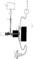
- the entire arrangement is placed on a Newport optical table research series plus.
- the arrangement comprises an argon-ion-laser 1 of the type Coherent Innova 400-20.
- the laser 1 may operated at the wavelengths 514.5 nm, 488 nm, 457.9 nm, 364 nm, and 351 nm. These wavelengths correspond to a photon energy less than the band gap of lithium niobate at 300°K.
- a number of optical components are arranged successive to the laser 1.
- the first component is a mirror of the type optics for Research, MYU-25-UV7 followed by a beam expander 4 comprising two lenses having a predetermined distance.
- the first lens is of the type LLU-25-63 N-A4, while the second lens is of the type LLU-25-190-A3.
- Two mirrors are next in line mounted on a damped rod, whereby the resolution may be increased during a laser-assisted etching in e.g. Si.
- the mirrors are of the type MYU-25-UV7.
- a lens 6 Optics for Research LLU-25-80-Al, focusing on the sample.
- the minimum obtainable spot size by means of this lens is approx. 8 ⁇ m, the heated area, however, corresponds to a spot size of approx. 20 ⁇ m.
- a spot size on 1/2-1 ⁇ m (for 351 nm) can be obtained by substituting the lens with a microscope objective of the type Ealing Electro-optics 25-0522.
- the sample is placed in a vacuum-sealed chamber 8 made of stainless steel and provided with a 1.5 mm thick quartz window. The distance between the sample and the window is approximately 3 mm.
- the focusing lens 6 is mounted on a Newport Z-stage, PM500 mini stage.
- this Z-stage is mounted on an arrangement of shock-absorbing rods and the like.
- the Z-stage can be adjusted with an accuracy of 25 nm and has a maximum scan length of 1 inch.
- the process chamber 8 is attached to a Newport X-Y-stage, PM500 regular, also adjustable with an accuracy of 25 nm and having a maximum scan length of 4 inches.
- This X-Y-stage can be moved at a rate from 0.1 ⁇ m/sec to 100mm/sec, and said Z-stage and X-Y-stage may be computerized.
- the process chamber 8 is connected with a nitrogen source 9 and a chlorine source 10.
- the chamber 8 may, if desired, be closed during processing or a gas may flow therethrough.
- the maximum gas flux is 10 sccm.
- the maximum chlorine gas pressure is approximately 750 mbar.
- such a chlorine gas pressure is inconvenient, as the gas absorbs some of the laser light at wavelengths of about 351 nm. Such a high pressure is not necessary to obtain high removal rates.
- the material ABO3, wherein A is an alkali or an alkaline earth metal and B is an transition metal may be processed by means of a CW-laser light with a photon energy being less than the band gap energy.
- an Ar-ion-laser on 351/364 nm or a Kr-ion-laser (330 nm) is used.
Applications Claiming Priority (6)
| Application Number | Priority Date | Filing Date | Title |
|---|---|---|---|
| DK50394 | 1994-05-03 | ||
| DK503/94 | 1994-05-03 | ||
| DK50394 | 1994-05-03 | ||
| DK1219/94 | 1994-10-20 | ||
| DK121994 | 1994-10-20 | ||
| DK121994A DK121994A (da) | 1994-05-03 | 1994-10-20 | Fremgangsmåde til bearbejdning af oxidmaterialer ved hjælp af en laserstråle |
Publications (2)
| Publication Number | Publication Date |
|---|---|
| EP0680804A1 true EP0680804A1 (de) | 1995-11-08 |
| EP0680804B1 EP0680804B1 (de) | 1998-07-29 |
Family
ID=26064122
Family Applications (1)
| Application Number | Title | Priority Date | Filing Date |
|---|---|---|---|
| EP95610024A Expired - Lifetime EP0680804B1 (de) | 1994-05-03 | 1995-05-03 | Verfahren zur Bearbeitung von oxidischen Materialien mittels eines Laserstrahls |
Country Status (4)
| Country | Link |
|---|---|
| EP (1) | EP0680804B1 (de) |
| AT (1) | ATE168913T1 (de) |
| DE (1) | DE69503693T2 (de) |
| DK (1) | DK121994A (de) |
Cited By (2)
| Publication number | Priority date | Publication date | Assignee | Title |
|---|---|---|---|---|
| EP0900660A2 (de) * | 1997-08-27 | 1999-03-10 | Canon Kabushiki Kaisha | Verfahren zur Herstellung von Flüssigkeitsstrahlaufzeichnungsköpfen und mit diesem Verfahren hergestellter Kopf |
| WO2024040142A3 (en) * | 2022-08-17 | 2024-03-21 | Nielson Scientific Llc | Parallelized three-dimensional semiconductor fabrication |
Citations (6)
| Publication number | Priority date | Publication date | Assignee | Title |
|---|---|---|---|---|
| JPS62136578A (ja) * | 1985-12-10 | 1987-06-19 | Nec Corp | ニオブ酸リチウム基板の加工方法 |
| JPS62180088A (ja) * | 1986-02-04 | 1987-08-07 | Nec Corp | レ−ザ加工方法およびレ−ザ加工装置 |
| DE3718323A1 (de) * | 1987-06-01 | 1988-12-22 | Siemens Ag | Verfahren zur oberflaechenbearbeitung, zum schneiden und dgl. von koerpern aus oxidwerkstoff |
| US4838989A (en) * | 1987-08-25 | 1989-06-13 | The United States Of America As Represented By The United States Department Of Energy | Laser-driven fusion etching process |
| EP0391848A1 (de) * | 1989-04-06 | 1990-10-10 | Ciba-Geigy Ag | Laserbeschriftung von keramischen Materialien, Glasuren, keramischen Gläsern und Gläsern |
| JPH04357133A (ja) * | 1990-12-20 | 1992-12-10 | Seikosha Co Ltd | 感光性ガラスの加工方法 |
-
1994
- 1994-10-20 DK DK121994A patent/DK121994A/da not_active Application Discontinuation
-
1995
- 1995-05-03 EP EP95610024A patent/EP0680804B1/de not_active Expired - Lifetime
- 1995-05-03 DE DE69503693T patent/DE69503693T2/de not_active Expired - Fee Related
- 1995-05-03 AT AT95610024T patent/ATE168913T1/de not_active IP Right Cessation
Patent Citations (6)
| Publication number | Priority date | Publication date | Assignee | Title |
|---|---|---|---|---|
| JPS62136578A (ja) * | 1985-12-10 | 1987-06-19 | Nec Corp | ニオブ酸リチウム基板の加工方法 |
| JPS62180088A (ja) * | 1986-02-04 | 1987-08-07 | Nec Corp | レ−ザ加工方法およびレ−ザ加工装置 |
| DE3718323A1 (de) * | 1987-06-01 | 1988-12-22 | Siemens Ag | Verfahren zur oberflaechenbearbeitung, zum schneiden und dgl. von koerpern aus oxidwerkstoff |
| US4838989A (en) * | 1987-08-25 | 1989-06-13 | The United States Of America As Represented By The United States Department Of Energy | Laser-driven fusion etching process |
| EP0391848A1 (de) * | 1989-04-06 | 1990-10-10 | Ciba-Geigy Ag | Laserbeschriftung von keramischen Materialien, Glasuren, keramischen Gläsern und Gläsern |
| JPH04357133A (ja) * | 1990-12-20 | 1992-12-10 | Seikosha Co Ltd | 感光性ガラスの加工方法 |
Non-Patent Citations (4)
| Title |
|---|
| CHEMICAL ABSTRACTS, vol. 119, no. 6, 9 August 1993, Columbus, Ohio, US; abstract no. 54609z, page 339; * |
| DATABASE WPI Section Ch Week 8730, Derwent World Patents Index; Class L03, AN 87-209798 * |
| PATENT ABSTRACTS OF JAPAN vol. 12, no. 33 (C - 472) 30 January 1988 (1988-01-30) * |
| R.W. DREYFUS ET AL, APPLIED PHYSICS LETTERS, vol. 50, no. 21, pages 1491 - 1493 * |
Cited By (4)
| Publication number | Priority date | Publication date | Assignee | Title |
|---|---|---|---|---|
| EP0900660A2 (de) * | 1997-08-27 | 1999-03-10 | Canon Kabushiki Kaisha | Verfahren zur Herstellung von Flüssigkeitsstrahlaufzeichnungsköpfen und mit diesem Verfahren hergestellter Kopf |
| EP0900660A3 (de) * | 1997-08-27 | 1999-09-15 | Canon Kabushiki Kaisha | Verfahren zur Herstellung von Flüssigkeitsstrahlaufzeichnungsköpfen und mit diesem Verfahren hergestellter Kopf |
| US6225032B1 (en) | 1997-08-27 | 2001-05-01 | Canon Kabushiki Kaisha | Method for manufacturing liquid jet recording heads and a head manufactured by such method of manufacture |
| WO2024040142A3 (en) * | 2022-08-17 | 2024-03-21 | Nielson Scientific Llc | Parallelized three-dimensional semiconductor fabrication |
Also Published As
| Publication number | Publication date |
|---|---|
| DK121994A (da) | 1995-11-04 |
| DE69503693D1 (de) | 1998-09-03 |
| EP0680804B1 (de) | 1998-07-29 |
| ATE168913T1 (de) | 1998-08-15 |
| DE69503693T2 (de) | 1999-01-07 |
Similar Documents
| Publication | Publication Date | Title |
|---|---|---|
| US5800625A (en) | Removal of material by radiation applied at an oblique angle | |
| US8890027B2 (en) | Laser processing method and laser processing system | |
| JP3033120B2 (ja) | 半導体薄膜の製造方法 | |
| US6566628B2 (en) | Method and device for thin-film ablation of a substrate | |
| WO2006035870A1 (ja) | レーザ加工方法及びレーザ加工装置 | |
| JPH08195357A (ja) | レーザー照射装置 | |
| WO2002022301A1 (fr) | Procede et dispositif d'usinage par rayonnement laser | |
| TW201531361A (zh) | 藉由叢發超快雷射脈衝之絲化雷射加工矽之方法及裝置 | |
| JP2014007375A (ja) | 回路個片化システム及び方法 | |
| JP2004515365A (ja) | 半導体材料のレーザー加工 | |
| KR20060126665A (ko) | 레이저 박막 폴리실리콘 어닐링 시스템 | |
| CA2604641A1 (en) | Method for finely polishing/structuring thermosensitive dielectric materials by a laser beam | |
| WO2004080643A1 (ja) | レーザ加工方法 | |
| EP2116323B1 (de) | Verfahren zur Herstellung eines Halbleiter-Wafers | |
| JP4762458B2 (ja) | レーザ加工装置 | |
| US5310990A (en) | Method of laser processing ferroelectric materials | |
| KR20070120491A (ko) | 회절 격자의 레이저 손상 임계치를 증가시키는 방법 | |
| JPH05226790A (ja) | レーザアニール装置 | |
| US6518539B2 (en) | Method for producing damage resistant optics | |
| JP2006007619A (ja) | レーザ加工方法及びレーザ加工装置 | |
| JP2587020B2 (ja) | ペロブスカイト型構造の酸化物材料の表面加工方法 | |
| JP3935187B2 (ja) | レーザ加工方法 | |
| EP0680804B1 (de) | Verfahren zur Bearbeitung von oxidischen Materialien mittels eines Laserstrahls | |
| Christensen et al. | Sub‐band‐gap laser micromachining of lithium niobate | |
| JP3935188B2 (ja) | レーザ加工装置 |
Legal Events
| Date | Code | Title | Description |
|---|---|---|---|
| PUAI | Public reference made under article 153(3) epc to a published international application that has entered the european phase |
Free format text: ORIGINAL CODE: 0009012 |
|
| AK | Designated contracting states |
Kind code of ref document: A1 Designated state(s): AT BE CH DE ES FR GB GR IE IT LI NL SE |
|
| 17P | Request for examination filed |
Effective date: 19960422 |
|
| GRAG | Despatch of communication of intention to grant |
Free format text: ORIGINAL CODE: EPIDOS AGRA |
|
| 17Q | First examination report despatched |
Effective date: 19970811 |
|
| GRAG | Despatch of communication of intention to grant |
Free format text: ORIGINAL CODE: EPIDOS AGRA |
|
| GRAH | Despatch of communication of intention to grant a patent |
Free format text: ORIGINAL CODE: EPIDOS IGRA |
|
| RAP1 | Party data changed (applicant data changed or rights of an application transferred) |
Owner name: AMP DANMARK, FILIAL AF AMP-HOLLAND B.V., HOLLAND |
|
| GRAH | Despatch of communication of intention to grant a patent |
Free format text: ORIGINAL CODE: EPIDOS IGRA |
|
| RAP1 | Party data changed (applicant data changed or rights of an application transferred) |
Owner name: THE WHITAKER CORPORATION |
|
| GRAA | (expected) grant |
Free format text: ORIGINAL CODE: 0009210 |
|
| AK | Designated contracting states |
Kind code of ref document: B1 Designated state(s): AT BE CH DE ES FR GB GR IE IT LI NL SE |
|
| PG25 | Lapsed in a contracting state [announced via postgrant information from national office to epo] |
Ref country code: LI Free format text: LAPSE BECAUSE OF FAILURE TO SUBMIT A TRANSLATION OF THE DESCRIPTION OR TO PAY THE FEE WITHIN THE PRESCRIBED TIME-LIMIT Effective date: 19980729 Ref country code: GR Free format text: LAPSE BECAUSE OF NON-PAYMENT OF DUE FEES Effective date: 19980729 Ref country code: ES Free format text: THE PATENT HAS BEEN ANNULLED BY A DECISION OF A NATIONAL AUTHORITY Effective date: 19980729 Ref country code: CH Free format text: LAPSE BECAUSE OF FAILURE TO SUBMIT A TRANSLATION OF THE DESCRIPTION OR TO PAY THE FEE WITHIN THE PRESCRIBED TIME-LIMIT Effective date: 19980729 Ref country code: BE Free format text: LAPSE BECAUSE OF FAILURE TO SUBMIT A TRANSLATION OF THE DESCRIPTION OR TO PAY THE FEE WITHIN THE PRESCRIBED TIME-LIMIT Effective date: 19980729 Ref country code: AT Free format text: LAPSE BECAUSE OF FAILURE TO SUBMIT A TRANSLATION OF THE DESCRIPTION OR TO PAY THE FEE WITHIN THE PRESCRIBED TIME-LIMIT Effective date: 19980729 |
|
| REF | Corresponds to: |
Ref document number: 168913 Country of ref document: AT Date of ref document: 19980815 Kind code of ref document: T |
|
| REG | Reference to a national code |
Ref country code: CH Ref legal event code: EP |
|
| REF | Corresponds to: |
Ref document number: 69503693 Country of ref document: DE Date of ref document: 19980903 |
|
| ITF | It: translation for a ep patent filed |
Owner name: BUZZI, NOTARO&ANTONIELLI D'OULX |
|
| ET | Fr: translation filed | ||
| REG | Reference to a national code |
Ref country code: IE Ref legal event code: FG4D |
|
| REG | Reference to a national code |
Ref country code: CH Ref legal event code: PL |
|
| PGFP | Annual fee paid to national office [announced via postgrant information from national office to epo] |
Ref country code: NL Payment date: 19990322 Year of fee payment: 5 |
|
| PGFP | Annual fee paid to national office [announced via postgrant information from national office to epo] |
Ref country code: GB Payment date: 19990406 Year of fee payment: 5 |
|
| PG25 | Lapsed in a contracting state [announced via postgrant information from national office to epo] |
Ref country code: IE Free format text: LAPSE BECAUSE OF NON-PAYMENT OF DUE FEES Effective date: 19990503 |
|
| PG25 | Lapsed in a contracting state [announced via postgrant information from national office to epo] |
Ref country code: SE Free format text: LAPSE BECAUSE OF NON-PAYMENT OF DUE FEES Effective date: 19990504 |
|
| PGFP | Annual fee paid to national office [announced via postgrant information from national office to epo] |
Ref country code: FR Payment date: 19990504 Year of fee payment: 5 |
|
| PGFP | Annual fee paid to national office [announced via postgrant information from national office to epo] |
Ref country code: DE Payment date: 19990531 Year of fee payment: 5 |
|
| PLBE | No opposition filed within time limit |
Free format text: ORIGINAL CODE: 0009261 |
|
| STAA | Information on the status of an ep patent application or granted ep patent |
Free format text: STATUS: NO OPPOSITION FILED WITHIN TIME LIMIT |
|
| 26N | No opposition filed | ||
| EUG | Se: european patent has lapsed |
Ref document number: 95610024.2 |
|
| REG | Reference to a national code |
Ref country code: GB Ref legal event code: 732E |
|
| PG25 | Lapsed in a contracting state [announced via postgrant information from national office to epo] |
Ref country code: GB Free format text: LAPSE BECAUSE OF NON-PAYMENT OF DUE FEES Effective date: 20000503 |
|
| PG25 | Lapsed in a contracting state [announced via postgrant information from national office to epo] |
Ref country code: NL Free format text: LAPSE BECAUSE OF NON-PAYMENT OF DUE FEES Effective date: 20001201 |
|
| GBPC | Gb: european patent ceased through non-payment of renewal fee |
Effective date: 20000503 |
|
| PG25 | Lapsed in a contracting state [announced via postgrant information from national office to epo] |
Ref country code: FR Free format text: LAPSE BECAUSE OF NON-PAYMENT OF DUE FEES Effective date: 20010131 |
|
| NLV4 | Nl: lapsed or anulled due to non-payment of the annual fee |
Effective date: 20001201 |
|
| PG25 | Lapsed in a contracting state [announced via postgrant information from national office to epo] |
Ref country code: DE Free format text: LAPSE BECAUSE OF NON-PAYMENT OF DUE FEES Effective date: 20010301 |
|
| REG | Reference to a national code |
Ref country code: FR Ref legal event code: ST |
|
| PG25 | Lapsed in a contracting state [announced via postgrant information from national office to epo] |
Ref country code: IT Free format text: LAPSE BECAUSE OF NON-PAYMENT OF DUE FEES Effective date: 20050503 |