EP0680203A2 - Abtastsystem zur Aufnahme oder Wiedergabe von Bildern - Google Patents
Abtastsystem zur Aufnahme oder Wiedergabe von Bildern Download PDFInfo
- Publication number
- EP0680203A2 EP0680203A2 EP94117766A EP94117766A EP0680203A2 EP 0680203 A2 EP0680203 A2 EP 0680203A2 EP 94117766 A EP94117766 A EP 94117766A EP 94117766 A EP94117766 A EP 94117766A EP 0680203 A2 EP0680203 A2 EP 0680203A2
- Authority
- EP
- European Patent Office
- Prior art keywords
- image
- mirror
- detector
- plane
- photodetector
- Prior art date
- Legal status (The legal status is an assumption and is not a legal conclusion. Google has not performed a legal analysis and makes no representation as to the accuracy of the status listed.)
- Granted
Links
Images


Classifications
-
- H—ELECTRICITY
- H04—ELECTRIC COMMUNICATION TECHNIQUE
- H04N—PICTORIAL COMMUNICATION, e.g. TELEVISION
- H04N3/00—Scanning details of television systems; Combination thereof with generation of supply voltages
- H04N3/02—Scanning details of television systems; Combination thereof with generation of supply voltages by optical-mechanical means only
- H04N3/08—Scanning details of television systems; Combination thereof with generation of supply voltages by optical-mechanical means only having a moving reflector
Definitions
- the invention relates generally to the field of imaging systems.
- CCD charged coupled devices
- Linear photodetectors cost much less than array detectors because they are much smaller and have higher manufacturing yields.
- the problem with linear photodetectors is that they resolve only one line of pixels at a time and must scan the entire image, line by line, within the exposure time of the camera.
- the exposure time of hand held cameras must be less than 1/15 of a second because users cannot hold cameras still for longer than this. Ideally, the exposure time is much shorter, such as 1/125 of a second.
- Previously known hand held cameras cannot use linear photodetectors because they cannot scan the linear detector across the entire image within their exposure time and because the linear photodetectors do not capture sufficient photons to produce a high quality image. If a previously known hand held camera were able to scan the linear detector across the entire image within its exposure time, the linear photodetector would be traveling at such high velocities and accelerations that it would jerk the camera out of the hands of the user.
- This invention is a system for capturing an image that has a lens to form an image on an image plane, a detector mounted to preclude translational motion, a mirror for deflecting the image to the plane of the detector, and a mechanism that moves the mirror to scan the image across the detector.
- the plane of the mirror “bisects" (i.e., divides into two equal parts) at 90°, an imaginary line between a cell on the detector that captured a portion of the image called here a "bundle of light' and a corresponding focal point on the image plane (i.e., the bundle of light that focuses on the cell of the detector has another focal point on the image plane called the corresponding focal point).
- the image capture system can capture "images" produced by electromagnetic waves of any frequency and it is adaptable to many different devices, for example: photocopiers, hand-held still cameras, motion picture cameras, film scanners, scanners connected to printers to form copiers, fax machines, scanners connected to memory for storing images, scanners connected to computers for altering images, microscopes, telescopes, coherent optics systems, and many other systems.
- This image capture system has the advantage that the motion of the detector and the motion of the mirror are minimized; and it can use inexpensive linear photodetectors, such as linear CCD photodetectors, to capture high-quality images.
- the image projection system is similar to the image capture system except that it operates in reverse and has an array of light generation elements instead of a light detector.
- the image projection system has light generation elements mounted to preclude translational motion, a mirror for deflecting the image, and a mechanism that moves the mirror to scan the image.
- a mirror plane bisects at 90°, an imaginary line between a cell on the light generation element that generates a portion of the image called the "bundle of light" and a corresponding focal point on the image plane (i.e., the bundle of light that originates from the photoemitter has another focal point on the image called the corresponding focal point).
- Figures 1A and 1B are three dimensional drawings that show the operation of the preferred embodiment of the image capture system.
- Figures 2A, 2B, and 2C are top views of the image capture system shown in Figures 1A and 1B with the mirror at three different positions in its trajectory.
- Figure 3 is a top view of the trajectory of the mirror shown in Figures 1A, 1B, and 2A-2C as the mirror scans an image onto the linear detectors.
- Figure 4 shows an alternative location of the photodetectors that provides space for the construction of baffles or other device.
- Figure 5 shows the preferred embodiment of the photodetectors.
- Figure 6 shows an alternate embodiment of the photodetectors.
- Figure 7 is a block diagram of an image acquisition system using the image capture system shown in Figures 1-4.
- Figure 8 is a block diagram of an image projection system.
- Figure 9 is a three dimensional drawing that shows the operation of the image projection system.
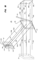
- FIG. 1A is a three dimensional diagram that shows the operation of the image capture system 20.
- Each bundle of light has a principal ray 33 (i.e., a light beam in the center of the bundle) and many auxiliary rays represented by auxiliary rays 34A-34D that come into focus at a position known as the corresponding focal point 36 on image plane 38.
- image capture system 20 the bundle of light that focuses on a corresponding focal point 36 on image plane 38 passes through an "image forming system" 24 (i.e., any of many systems for focusing an image on image plane 38, such as, a telescope, a periscope, a microscope, a single lens, holographic lens, a coherent optic system, telephoto lens, a mirror, an image stabilizer, a filter, as well as many other devices.) Then, a mirror 26 deflects if from its path enroute to image plane 38 to a detector plane 31 and a detector 30 where it focuses on a cell 44. Tracks 48 represent one of many possible devices that control the trajectory of mirror 26.
- Tracks 48 represent one of many possible devices that control the trajectory of mirror 26.
- Figure 1B represents additional bundles of light solely by their principal rays 33, 33A, 33B, 33C, and 33D to simplify the drawings.
- Each bundle of light is detected by a different photocell 44, 44A, 44B, 44C, 44D and has a different corresponding focal point 36, 36A, 36B, 36C, 36D.
- a best mode of the invention uses linear TDI (i.e., time delay integration) photodetectors that have chains of horizontally integrated photocell stages that transfer charge between one another to increase the exposure time of the image capture system.
- TDI time delay integration
- mirror 26 scans the bundles of light represented by principal rays 33, 33A, 33B, 33C, and 33D across photodetector 30, electrical charges move synchronously from one photocell to another horizontally integrated photocell.
- Figure 5 shows an embodiment of photodetector 30. It has four groups of three TDI CCD detectors 32A, 32B, and 32C, each covered by a different filter so that each detects either a red, green, or blue light.
- Photodetectors can have filters of different colors without departing from the scope of the invention).
- the TDI detectors 32A, 32B, and 32C are mounted side-by-side and each TDI detector has approximately 100 stages that results in mirror 26 scanning the image over approximately 1200 stages while that photodetector 30 rotates at an angular speed that is twice that of mirror 26.
- Alternative embodiments of the invention may use any number of photodetectors or groups of three photodetectors without departing from the scope of the invention. Additionally, the photodetectors may be point detectors, linear detectors, or have any width without departing from the scope of the invention. Alternative embodiments of the invention may use any type of light sensitive material, even photofilm if it moves with mirror 26.
- Image capture system 20 limits the velocities and accelerations generated by the system by precluding translational motion of the detector and by making mirror 26 or a mirror plane 28 (i.e., mirror means refers to mirror 26 and/or mirror plane 28) bisect at 90° an imaginary line between cell 44 on detector 30 and its corresponding focal point 36 and by making photodetector 30 rotate synchronously with and at twice the rotational rate of mirror 26 when the width of detector 30 is greater than one cell.
- Figures 2A-2C and 3 describe this unique trajectory and rotation in more detail.
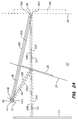
- Figure 2A is a top view of the best mode of image capture system 20 that illustrates the invention.
- Figures 2A-2C, 3, and 4 use only the principal ray to represent a bundle of light.
- the trajectory of mirror 26 results in mirror plane 28 bisecting at 90°, lines 46, 46A, and 46B that extend from photocells 44, 44A, and 44B to their corresponding focal points 36, 36A, and 36B.
- a result of this geometry is that the distance between mirror 26 and photocells 44, 44A, and 44B always equals the distance between mirror 26 and their corresponding focal points 36, 36A, and 36B.
- the advantage of this unique trajectory is that it minimizes the motion of mirror 26 and photodetector 30 so that mirror 26 can scan the image onto photodetectors 30 (that do not have translation motion) within the exposure time of the camera without generating unwieldy forces.
- the exposure time of the image capture system 20 will be at least partially determined by the device that uses it.
- Mirror plane 28 not only bisects lines 46, 46A, and 46B but it bisects all imaginary lines between all photocells and their corresponding focal points.
- the best mode of the invention uses four groups of three 100x2048 TDI photodetectors, as shown in Figure 5. Each group has 614,400 photocells, 614,400 corresponding focal points, and 614,400 lines between the photocells and the corresponding focal points that mirror plane 28 bisects at 90°.
- Figures 2B and 2C show that despite the position of mirror 26 in its trajectory, mirror plane 28 always bisects, at 90°, imaginary line 46 connecting photocell 44 and its corresponding focal point 40 or 42 on image plane 38.
- the position of mirror 26 causes it to deflect a bundle of light represented by principal ray 33 to photocell 44. This bundle of light would otherwise focus on a corresponding focal point 40 on image plane 38.
- mirror 26 reflects a bundle of light represented by principal ray 33 to photocell 44 that would otherwise focus on location 42 of image plane 38.
- mirror plane 28 always bisects, at 90°, imaginary line 46 between photocell 44 and corresponding focal point 36, 40, or 42 on image plane 38.
- mirror 26 reflects all light that strikes it and image plane 38 is not an actual device, but instead, an imaginary plane of focal points.
- mirror 26 moves out of the way or transmits some of the light that strikes it (e.g., 25%). This light travels to the position of image plane 38 where it focuses on a secondary device 68 (shown in outline form on Figures 2A, 2B, and 2C), such as an autofocus sensor, contrast ratio sensor, automatic exposure sensor, viewfinder, or other device that would inspect the incoming image and adjust the camera.
- a secondary device 68 shown in outline form on Figures 2A, 2B, and 2C
- some alternative embodiments of the invention have two or more light sensitive devices at two or more focal planes.
- Figure 3 shows various positions of mirror plane 28, as it scans the image onto photodetector 30.
- the distance between mirror plane 28 and photocell 44 equals the distance between mirror plane 28 and corresponding focal point 36, 40, or 42 on image plane 38 though that distance changes as mirror 26 moves.
- Mirror plane 28 always bisects imaginary line 46 (not shown for clarity) at 90°.
- Figures 2A, 2B, and 2C and Figure 3 show the synchronization between the movement of mirror 26 and the rotation of photodetector 30 such that photodetector 30 rotates twice as much as mirror 26 when photodetector 30 has a width greater than one photocell.
- photodetector 30 has a width of one photocell, such as a point detector or a linear detector, and it does not rotate.
- Figure 4 shows image capture system 20 with photodetector 30 in alternative positions.
- Mirror plane 28 still bisects line 46 at 90°.
- photodetectors 30 can reside in a variety of positions.
- photodetectors 30 can be positioned to minimize the effect of stray light by constructing baffles near photodetector 30.
- TDI CCD linear photodetector 32A, 32B, 32C, shown in Figure 5 is the IT-E1 Series TDI QuietsensorTM available from Dalsa Inc., Waterloo, Ontario, Canada (Phone: 519-886-6000).
- Mirror 26 with its unique trajectory may be used with any type of photodetector.
- a single 1 x 2048 photodetector may be used for capturing black and white images.
- Other photodetectors and photosensitive films can be used without departing from the scope of the invention.
- other configurations of photosensitive devices such as the mosaic photodetector shown in Figure 6, can be used without departing from the scope of the invention.
- Each TDI photodetector 32A, 32B, 32C used in the best mode of this invention is an array of photocells having a height of 2048 rows of photocells and a width of 96 photocells connected so electrical charges created in one photocell transfers to a neighboring photocell at a specified time interval.
- Alternative embodiments of the invention may use other types of photodetectors with sizes other than 96x2048 without departing from the scope of the invention.
- a detector controller 66 and a camera controller 58 shown in Figure 7 synchronize the transfer of charges between photocells with the motion of mirror 26 and thereby with the motion of the image across TDI detector 30.
- a second photocell located adjacent to a first photocell converts photons from the same bundle of light into an electric charge and adds this to the electric charge transferred from the first photocell.
- the image capture system 20 repeats this 95 times across detector 30.
- the advantage of using TDI CCD linear detectors 32A, 32B, 32C is that they effectively give the image a longer exposure. This results in a higher effective sensitivity to light and a greater spatial uniformity and fidelity in the captured image. Additionally, it allows image capture system 20 to produce a high resolution/high quality image with less light.
- an array photodetector must have the dimensions of approximately 3000x2000 pixels to produce an image having a quality comparable to conventional 35mm chemical photography.
- the linear photodetector or TDI photodetector has a length of 1 x 2048 photocells, it must resolve the other dimension of the image into 3072 pixels. This is accomplished by scanning the image across photodetector 30.
- a 96 x 2048 TDI linear detector increases the length of the exposure by 96. Increasing the number of horizontally integrated photocells further lengthens the exposure.
- a 96x2048 TDI linear photodetector is much more effective than ninety-six 1x2048 linear photodetectors mounted side by side because the charge transfer mechanism within a chip has a much better signal-to-noise ratio then transferring an electric signal between chips.
- An alternative embodiment of the invention uses a mosaic photodetector 70 shown in Figure 6.
- Mosaics of photodetectors 70 may have the advantage of being inexpensive because they use many small photodetectors 72 that have high yields.
- Small photodetectors 72 can be time delay and integration (TDI) photodetectors having any dimensions, such as 256 rows of photocells, each row containing 96 photocells chained together.
- Photodetectors 72 are assembled onto multi-chip modules.
- mosaic photodetector 70 has the photodetectors arranged into columns with a red photodetector 76, then a green photodetector 78, then a blue photodetector 80, and the pattern repeats itself.
- image forming systems 24 may use an image stabilizer.
- Image stabilizers compensate for small deviations in the position of the camera so that the image projected onto mirror 26 remains stationary.
- the image stabilizer can be liquid baffles controlled by accelerometers, liquid deforming lens, gyro-controlled lens as well as other devices.
- signal processing techniques can be used on the digitized image to correct distortions introduced by this motion.
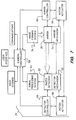
- Figure 7 shows a block diagram of a camera system that uses image capture system 20.
- a light image travels through image forming system 24 to mirror 26 that reflects it to photodetector 30.
- a mirror controller 68 receives commands from a camera controller 58, senses the position of mirror 26 and commands a motion actuator 56 to transmit power to a mirror mechanism 54.
- Mirror mechanism 54 uses this power to move mirror 26 along a trajectory that causes it to scan an image across detector 30 and that causes mirror plane 28 to bisect at 90° imaginary lines 46 that extend between cells 44 of detector 30 and their corresponding focal points 46.
- a detector controller 66 receives commands from camera controller 58, detects the position of photodetector 30, and commands motion actuator 56 to provide power to a detector mechanism 52 that causes detector 30 to rotate at twice the rotation speed of mirror 26.
- the output of photodetector 30 goes to a signal processing system 58 that combines the output of the photodetectors 30 to form a color image.
- Camera controller 58 coordinates the operation of the signal processing system 82 with the movement of mirror 26 and photodetectors 30.
- Detector 30 and mirror 26 can use the same motion actuator 56 or different motion actuators 56.
- Motion actuator 56 can be a motor, or a spring loaded mechanism, or other devices without departing from the scope of the invention.
- Detector mechanism 52 can be gears, pulleys, or other devices that cause the detector to rotate at the desired speed.
- Mirror mechanism 54 can be a mirror support attached to motor actuator 56 through gears, pulleys, or other devices to give it desired translational motion. Rotational motion can be achieved by tilting the mirror support when it has translational motion. This combination of translational and rotational motion can be achieved by a wide variety devices that one with ordinary skill in the art could design.
- Image capture system 20 can be installed in wide variety devices: photocopiers, hand-held still cameras, motion picture cameras, film scanners, scanners connected to printers to form a copier, fax machines, scanners connected to memory for storing the image, scanners connected to computers for altering the image, microscopes, telescopes, coherent optics systems, and many other image capture systems.
- the host device will determine what type of mass storage, user interface, and communications links will attach to image capture system 20.
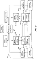
- FIG 8 is a block diagram of an image projection system 90 that is very similar to image capture system 20 shown in Figures 1A - Figure 7 with the exceptions being that it has light emitters 84 instead of detectors 30 and that it operates in reverse of image capture system 20.
- Mass storage 92 stores information that creates an image. This information is transmitted to signal processing system 82 by projector controller 94. Signal processing system 82 prepares this information for light emitters 84A, 84B, and 84C, each light emitter has a different color filter to produce as many as three different bundles of light for each portion of the image. If black and white images are produced than only one light emitter will be used.
- Projector controller 94 scans the image across light emitters 84A, 84B, and 84C.
- Mirror 26 intercepts these bundles of light and scans them across image forming system 24.
- the trajectory of mirror 26 for image projection system 90 is the same as the trajectory of mirror 26 for the image capture system shown in Figure 1A, 1B, 2, 3, and 4.
- Image formation system 24 focuses the bundles of light to form an image at a distant point.
- Figure 9 shows the path of a bundle of light in image projection system 90.
- a cell 86 of light emitter 84 emits a bundle of light containing a principal ray 33, and auxiliary rays 34A, 34B, 34C, and 34D.
- Mirror 26 deflects this bundle of light to image formation system 24 that focuses it on an distant plane.
Applications Claiming Priority (2)
| Application Number | Priority Date | Filing Date | Title |
|---|---|---|---|
| US236781 | 1994-04-29 | ||
| US08/236,781 US5481300A (en) | 1994-04-29 | 1994-04-29 | Image capture system |
Publications (3)
| Publication Number | Publication Date |
|---|---|
| EP0680203A2 true EP0680203A2 (de) | 1995-11-02 |
| EP0680203A3 EP0680203A3 (de) | 1996-03-13 |
| EP0680203B1 EP0680203B1 (de) | 1999-04-07 |
Family
ID=22890945
Family Applications (1)
| Application Number | Title | Priority Date | Filing Date |
|---|---|---|---|
| EP94117766A Expired - Lifetime EP0680203B1 (de) | 1994-04-29 | 1994-11-10 | Abtastsystem zur Aufnahme oder Wiedergabe von Bildern |
Country Status (4)
| Country | Link |
|---|---|
| US (2) | US5481300A (de) |
| EP (1) | EP0680203B1 (de) |
| JP (1) | JP3662625B2 (de) |
| DE (1) | DE69417723T2 (de) |
Cited By (1)
| Publication number | Priority date | Publication date | Assignee | Title |
|---|---|---|---|---|
| EP0796005A2 (de) * | 1996-03-11 | 1997-09-17 | Matsushita Electric Industrial Co., Ltd. | Elektronische Kamera mit einem kleinen Sensor für Hochgeschwindigkeitsbildaufnahme |
Families Citing this family (10)
| Publication number | Priority date | Publication date | Assignee | Title |
|---|---|---|---|---|
| EP0817476A3 (de) * | 1996-07-01 | 1998-05-13 | Sun Microsystems, Inc. | Fortgeschrittene elektronische Sucher für stehendes Bild |
| US6426776B1 (en) * | 1997-03-18 | 2002-07-30 | Minolta Co., Ltd. | Apparatus for and method of photographing using scanning techniques |
| US6124585A (en) * | 1998-10-27 | 2000-09-26 | Umm Electronics, Inc. | Apparatus for measuring the reflectance of strips having non-uniform color |
| US6160910A (en) | 1998-12-02 | 2000-12-12 | Freifeld; Daniel | High precision three dimensional mapping camera |
| US20030098918A1 (en) * | 1999-05-27 | 2003-05-29 | Miller Peter J. | Imaging system using color sensors and tunable filters |
| US6700606B1 (en) * | 1999-06-09 | 2004-03-02 | Activcard Ireland Limited | Micromirror optical imager |
| US6711283B1 (en) * | 2000-05-03 | 2004-03-23 | Aperio Technologies, Inc. | Fully automatic rapid microscope slide scanner |
| US6768510B2 (en) * | 2002-02-11 | 2004-07-27 | Nomadics, Inc. | Color correction for RGB |
| DE102004007911B3 (de) * | 2004-02-13 | 2005-02-03 | Deutsches Zentrum für Luft- und Raumfahrt e.V. | Vorrichtung zur digitalen Abtastung von farbigen Bildvorlagen |
| US7334349B2 (en) * | 2004-08-24 | 2008-02-26 | Nike, Inc. | Midsole element for an article of footwear |
Citations (2)
| Publication number | Priority date | Publication date | Assignee | Title |
|---|---|---|---|---|
| US5075539A (en) * | 1989-06-07 | 1991-12-24 | Fuji Xerox Co., Ltd. | Method and apparatus for adjusting the position of image reading equipment |
| EP0576704A1 (de) * | 1992-06-30 | 1994-01-05 | CGK Computer Gesellschaft Konstanz mbH | Verfahren zur Aufbereitung von mehrfarbigen Bildvorlagen für die maschinelle optische Zeichenerkennung |
Family Cites Families (11)
| Publication number | Priority date | Publication date | Assignee | Title |
|---|---|---|---|---|
| US4129887A (en) * | 1977-10-31 | 1978-12-12 | General Electric Company | Solid stage imaging apparatus |
| DE2831296C2 (de) * | 1978-07-17 | 1984-12-20 | Agfa-Gevaert Ag, 5090 Leverkusen | Vorrichtung zum elektronischen Abtasten von Superacht-Filmen zur Darstellung auf einem Fernsehgerät |
| DE3133641A1 (de) * | 1981-08-26 | 1983-03-10 | Philips Patentverwaltung Gmbh, 2000 Hamburg | Ir-sichtgeraet |
| US4442457A (en) * | 1981-12-17 | 1984-04-10 | Hughes Aircraft Company | Charge coupled device focal zoom |
| US4516159A (en) * | 1983-03-03 | 1985-05-07 | Magnavox Government And Industrial Electronics, Co. | Elevation step scanner |
| DE3531666A1 (de) * | 1985-09-05 | 1987-03-12 | Zeiss Carl Fa | Vorrichtung zur erzeugung eines bildes einer szene, vorzugsweise eines waermebildes |
| FR2620287B1 (fr) * | 1987-09-04 | 1994-04-22 | Thomson Video Equip | Dispositif optique d'analyse d'images fixes en television et analyseur comportant un tel dispositif |
| US5032924A (en) * | 1989-04-10 | 1991-07-16 | Nilford Laboratories, Inc. | System for producing an image from a sequence of pixels |
| FR2660468B1 (fr) * | 1990-04-02 | 1992-07-24 | Sagem | Dispositif d'imagerie et de surveillance a detecteur matriciel. |
| AU8765891A (en) * | 1990-10-02 | 1992-04-28 | Patrick Foulgoc | Camera and projection device |
| US5212555A (en) * | 1991-12-17 | 1993-05-18 | Texas Instruments Incorporated | Image capture with spatial light modulator and single-cell photosensor |
-
1994
- 1994-04-29 US US08/236,781 patent/US5481300A/en not_active Expired - Lifetime
- 1994-11-10 EP EP94117766A patent/EP0680203B1/de not_active Expired - Lifetime
- 1994-11-10 DE DE69417723T patent/DE69417723T2/de not_active Expired - Fee Related
-
1995
- 1995-04-28 JP JP10527095A patent/JP3662625B2/ja not_active Expired - Fee Related
- 1995-09-27 US US08/534,779 patent/US5646683A/en not_active Expired - Lifetime
Patent Citations (2)
| Publication number | Priority date | Publication date | Assignee | Title |
|---|---|---|---|---|
| US5075539A (en) * | 1989-06-07 | 1991-12-24 | Fuji Xerox Co., Ltd. | Method and apparatus for adjusting the position of image reading equipment |
| EP0576704A1 (de) * | 1992-06-30 | 1994-01-05 | CGK Computer Gesellschaft Konstanz mbH | Verfahren zur Aufbereitung von mehrfarbigen Bildvorlagen für die maschinelle optische Zeichenerkennung |
Cited By (3)
| Publication number | Priority date | Publication date | Assignee | Title |
|---|---|---|---|---|
| EP0796005A2 (de) * | 1996-03-11 | 1997-09-17 | Matsushita Electric Industrial Co., Ltd. | Elektronische Kamera mit einem kleinen Sensor für Hochgeschwindigkeitsbildaufnahme |
| EP0796005A3 (de) * | 1996-03-11 | 1998-08-12 | Matsushita Electric Industrial Co., Ltd. | Elektronische Kamera mit einem kleinen Sensor für Hochgeschwindigkeitsbildaufnahme |
| US6005617A (en) * | 1996-03-11 | 1999-12-21 | Matsushita Electric Industrial Co., Ltd. | Electronic camera with mechanical subscanner |
Also Published As
| Publication number | Publication date |
|---|---|
| DE69417723D1 (de) | 1999-05-12 |
| US5646683A (en) | 1997-07-08 |
| JP3662625B2 (ja) | 2005-06-22 |
| JPH07307880A (ja) | 1995-11-21 |
| DE69417723T2 (de) | 1999-10-14 |
| EP0680203A3 (de) | 1996-03-13 |
| US5481300A (en) | 1996-01-02 |
| EP0680203B1 (de) | 1999-04-07 |
Similar Documents
| Publication | Publication Date | Title |
|---|---|---|
| US5561460A (en) | Solid-state image pick up device having a rotating plate for shifting position of the image on a sensor array | |
| US5774179A (en) | Method and system for fast microscanning | |
| US6987258B2 (en) | Integrated circuit-based compound eye image sensor using a light pipe bundle | |
| EP0109249A2 (de) | Strahlungsnachweisgerät | |
| US5646683A (en) | Imaging systems | |
| EP0947091A1 (de) | System und verfahren zur bildbewegungskompensation eines ccd-bildsensors | |
| JPH1169209A (ja) | 撮像装置 | |
| EP0899944B1 (de) | Bildaufnahmegerät mit Bildpunktverschiebung | |
| KR100516892B1 (ko) | 멀티빔 광학주사장치 및 화상 형성장치와 그것을 이용한컬러화상 형성장치 | |
| US5025313A (en) | System for minimizing optical distortions and chromatic aberrations in a linear color scanner | |
| US4314150A (en) | Apparatus for detecting the in-focusing conditions | |
| EP0057584B1 (de) | Optischer Bildabtaster | |
| US6486938B1 (en) | Line exposure type image forming apparatus | |
| US20040012705A1 (en) | Distortion-free imaging device having curved photosensor | |
| US6771310B1 (en) | Image pickup apparatus with optical beam shifting with independently controlled optical elements | |
| JP2000514970A (ja) | 高速高解像度イメージキャプチャ装置 | |
| US6593559B2 (en) | Image readout apparatus and image readout method using the same | |
| US4958241A (en) | Image input apparatus | |
| USH1740H (en) | Synchronized rotating prism and CCD electrical readout color camera | |
| JP2003008997A (ja) | 撮像素子及び撮像素子を用いたデジタルスチルカメラ | |
| KR100263425B1 (ko) | 고정밀도의 촬상장치 | |
| JPH06139340A (ja) | 画像生成方法および撮像装置 | |
| JPS63193678A (ja) | 二次元固体撮像装置 | |
| EP0238111B1 (de) | Kamera zur Aufnahme von Fernsehbildern, photographischen oder kinematographischen Bildern mit automatischer Fokussierungsvorrichtung | |
| CN115218812A (zh) | 深度数据测量头、计算装置及其对应方法 |
Legal Events
| Date | Code | Title | Description |
|---|---|---|---|
| PUAI | Public reference made under article 153(3) epc to a published international application that has entered the european phase |
Free format text: ORIGINAL CODE: 0009012 |
|
| AK | Designated contracting states |
Kind code of ref document: A2 Designated state(s): DE FR GB |
|
| PUAL | Search report despatched |
Free format text: ORIGINAL CODE: 0009013 |
|
| AK | Designated contracting states |
Kind code of ref document: A3 Designated state(s): DE FR GB |
|
| 17P | Request for examination filed |
Effective date: 19960913 |
|
| 17Q | First examination report despatched |
Effective date: 19970624 |
|
| GRAG | Despatch of communication of intention to grant |
Free format text: ORIGINAL CODE: EPIDOS AGRA |
|
| GRAG | Despatch of communication of intention to grant |
Free format text: ORIGINAL CODE: EPIDOS AGRA |
|
| GRAG | Despatch of communication of intention to grant |
Free format text: ORIGINAL CODE: EPIDOS AGRA |
|
| GRAH | Despatch of communication of intention to grant a patent |
Free format text: ORIGINAL CODE: EPIDOS IGRA |
|
| GRAH | Despatch of communication of intention to grant a patent |
Free format text: ORIGINAL CODE: EPIDOS IGRA |
|
| GRAA | (expected) grant |
Free format text: ORIGINAL CODE: 0009210 |
|
| AK | Designated contracting states |
Kind code of ref document: B1 Designated state(s): DE FR GB |
|
| REF | Corresponds to: |
Ref document number: 69417723 Country of ref document: DE Date of ref document: 19990512 |
|
| ET | Fr: translation filed | ||
| PLBE | No opposition filed within time limit |
Free format text: ORIGINAL CODE: 0009261 |
|
| STAA | Information on the status of an ep patent application or granted ep patent |
Free format text: STATUS: NO OPPOSITION FILED WITHIN TIME LIMIT |
|
| 26N | No opposition filed | ||
| REG | Reference to a national code |
Ref country code: GB Ref legal event code: 732E |
|
| REG | Reference to a national code |
Ref country code: FR Ref legal event code: TP |
|
| REG | Reference to a national code |
Ref country code: GB Ref legal event code: IF02 |
|
| PGFP | Annual fee paid to national office [announced via postgrant information from national office to epo] |
Ref country code: GB Payment date: 20070125 Year of fee payment: 13 |
|
| PGFP | Annual fee paid to national office [announced via postgrant information from national office to epo] |
Ref country code: DE Payment date: 20070228 Year of fee payment: 13 |
|
| PGFP | Annual fee paid to national office [announced via postgrant information from national office to epo] |
Ref country code: FR Payment date: 20070423 Year of fee payment: 13 |
|
| GBPC | Gb: european patent ceased through non-payment of renewal fee |
Effective date: 20071110 |
|
| PG25 | Lapsed in a contracting state [announced via postgrant information from national office to epo] |
Ref country code: DE Free format text: LAPSE BECAUSE OF NON-PAYMENT OF DUE FEES Effective date: 20080603 |
|
| REG | Reference to a national code |
Ref country code: FR Ref legal event code: ST Effective date: 20080930 |
|
| PG25 | Lapsed in a contracting state [announced via postgrant information from national office to epo] |
Ref country code: GB Free format text: LAPSE BECAUSE OF NON-PAYMENT OF DUE FEES Effective date: 20071110 |
|
| PG25 | Lapsed in a contracting state [announced via postgrant information from national office to epo] |
Ref country code: FR Free format text: LAPSE BECAUSE OF NON-PAYMENT OF DUE FEES Effective date: 20071130 |