EP0675552B1 - Lichtemittierende Halbleitervorrichtung mit Verbindung aus Stickstoff und Elementen der Gruppe III - Google Patents
Lichtemittierende Halbleitervorrichtung mit Verbindung aus Stickstoff und Elementen der Gruppe III Download PDFInfo
- Publication number
- EP0675552B1 EP0675552B1 EP95104140A EP95104140A EP0675552B1 EP 0675552 B1 EP0675552 B1 EP 0675552B1 EP 95104140 A EP95104140 A EP 95104140A EP 95104140 A EP95104140 A EP 95104140A EP 0675552 B1 EP0675552 B1 EP 0675552B1
- Authority
- EP
- European Patent Office
- Prior art keywords
- layer
- doped
- emission layer
- emission
- semiconductor device
- Prior art date
- Legal status (The legal status is an assumption and is not a legal conclusion. Google has not performed a legal analysis and makes no representation as to the accuracy of the status listed.)
- Expired - Lifetime
Links
- 239000004065 semiconductor Substances 0.000 title claims description 27
- 229910017464 nitrogen compound Inorganic materials 0.000 title description 2
- 150000002830 nitrogen compounds Chemical class 0.000 title description 2
- 239000012535 impurity Substances 0.000 claims description 41
- PXHVJJICTQNCMI-UHFFFAOYSA-N Nickel Chemical compound [Ni] PXHVJJICTQNCMI-UHFFFAOYSA-N 0.000 claims description 36
- JMASRVWKEDWRBT-UHFFFAOYSA-N Gallium nitride Chemical compound [Ga]#N JMASRVWKEDWRBT-UHFFFAOYSA-N 0.000 claims description 27
- 229910002601 GaN Inorganic materials 0.000 claims description 26
- 229910052710 silicon Inorganic materials 0.000 claims description 14
- 229910052759 nickel Inorganic materials 0.000 claims description 12
- -1 nitride compound Chemical class 0.000 claims description 9
- XUIMIQQOPSSXEZ-UHFFFAOYSA-N Silicon Chemical compound [Si] XUIMIQQOPSSXEZ-UHFFFAOYSA-N 0.000 claims description 6
- 239000010703 silicon Substances 0.000 claims description 6
- 125000005842 heteroatom Chemical group 0.000 claims description 5
- RNQKDQAVIXDKAG-UHFFFAOYSA-N aluminum gallium Chemical compound [Al].[Ga] RNQKDQAVIXDKAG-UHFFFAOYSA-N 0.000 claims description 4
- 150000001875 compounds Chemical class 0.000 claims description 4
- JBQYATWDVHIOAR-UHFFFAOYSA-N tellanylidenegermanium Chemical compound [Te]=[Ge] JBQYATWDVHIOAR-UHFFFAOYSA-N 0.000 claims description 4
- 229910052782 aluminium Inorganic materials 0.000 claims description 3
- 239000011777 magnesium Substances 0.000 description 28
- QGZKDVFQNNGYKY-UHFFFAOYSA-N Ammonia Chemical compound N QGZKDVFQNNGYKY-UHFFFAOYSA-N 0.000 description 19
- 239000011701 zinc Substances 0.000 description 19
- 229910000069 nitrogen hydride Inorganic materials 0.000 description 17
- 239000000758 substrate Substances 0.000 description 14
- 229910052594 sapphire Inorganic materials 0.000 description 12
- 239000010980 sapphire Substances 0.000 description 12
- BLRPTPMANUNPDV-UHFFFAOYSA-N Silane Chemical compound [SiH4] BLRPTPMANUNPDV-UHFFFAOYSA-N 0.000 description 11
- 238000004519 manufacturing process Methods 0.000 description 11
- 238000000034 method Methods 0.000 description 11
- 239000013256 coordination polymer Substances 0.000 description 10
- 229910000077 silane Inorganic materials 0.000 description 10
- 229910052725 zinc Inorganic materials 0.000 description 10
- 229910052793 cadmium Inorganic materials 0.000 description 9
- 238000010586 diagram Methods 0.000 description 8
- 238000010894 electron beam technology Methods 0.000 description 8
- 229910052749 magnesium Inorganic materials 0.000 description 8
- 229920002120 photoresistant polymer Polymers 0.000 description 8
- 230000008569 process Effects 0.000 description 8
- 230000006798 recombination Effects 0.000 description 7
- 238000005215 recombination Methods 0.000 description 7
- VYPSYNLAJGMNEJ-UHFFFAOYSA-N Silicium dioxide Chemical compound O=[Si]=O VYPSYNLAJGMNEJ-UHFFFAOYSA-N 0.000 description 6
- KRHYYFGTRYWZRS-UHFFFAOYSA-N Fluorane Chemical compound F KRHYYFGTRYWZRS-UHFFFAOYSA-N 0.000 description 4
- HQWPLXHWEZZGKY-UHFFFAOYSA-N diethylzinc Chemical compound CC[Zn]CC HQWPLXHWEZZGKY-UHFFFAOYSA-N 0.000 description 4
- 230000001747 exhibiting effect Effects 0.000 description 4
- 239000007789 gas Substances 0.000 description 4
- 239000011669 selenium Substances 0.000 description 4
- 238000001228 spectrum Methods 0.000 description 4
- FYYHWMGAXLPEAU-UHFFFAOYSA-N Magnesium Chemical compound [Mg] FYYHWMGAXLPEAU-UHFFFAOYSA-N 0.000 description 3
- 229910052681 coesite Inorganic materials 0.000 description 3
- 229910052906 cristobalite Inorganic materials 0.000 description 3
- 238000010438 heat treatment Methods 0.000 description 3
- 229910052738 indium Inorganic materials 0.000 description 3
- 238000009413 insulation Methods 0.000 description 3
- 230000001678 irradiating effect Effects 0.000 description 3
- 239000007788 liquid Substances 0.000 description 3
- 230000007246 mechanism Effects 0.000 description 3
- 239000000377 silicon dioxide Substances 0.000 description 3
- 229910052682 stishovite Inorganic materials 0.000 description 3
- 229910052905 tridymite Inorganic materials 0.000 description 3
- CSCPPACGZOOCGX-UHFFFAOYSA-N Acetone Chemical compound CC(C)=O CSCPPACGZOOCGX-UHFFFAOYSA-N 0.000 description 2
- XKRFYHLGVUSROY-UHFFFAOYSA-N Argon Chemical compound [Ar] XKRFYHLGVUSROY-UHFFFAOYSA-N 0.000 description 2
- OKTJSMMVPCPJKN-UHFFFAOYSA-N Carbon Chemical compound [C] OKTJSMMVPCPJKN-UHFFFAOYSA-N 0.000 description 2
- BUGBHKTXTAQXES-UHFFFAOYSA-N Selenium Chemical compound [Se] BUGBHKTXTAQXES-UHFFFAOYSA-N 0.000 description 2
- NINIDFKCEFEMDL-UHFFFAOYSA-N Sulfur Chemical compound [S] NINIDFKCEFEMDL-UHFFFAOYSA-N 0.000 description 2
- ATJFFYVFTNAWJD-UHFFFAOYSA-N Tin Chemical compound [Sn] ATJFFYVFTNAWJD-UHFFFAOYSA-N 0.000 description 2
- 238000000137 annealing Methods 0.000 description 2
- 229910052790 beryllium Inorganic materials 0.000 description 2
- ATBAMAFKBVZNFJ-UHFFFAOYSA-N beryllium atom Chemical compound [Be] ATBAMAFKBVZNFJ-UHFFFAOYSA-N 0.000 description 2
- BDOSMKKIYDKNTQ-UHFFFAOYSA-N cadmium atom Chemical compound [Cd] BDOSMKKIYDKNTQ-UHFFFAOYSA-N 0.000 description 2
- 229910052799 carbon Inorganic materials 0.000 description 2
- 239000000969 carrier Substances 0.000 description 2
- 230000007423 decrease Effects 0.000 description 2
- 238000001312 dry etching Methods 0.000 description 2
- 238000002003 electron diffraction Methods 0.000 description 2
- 238000005530 etching Methods 0.000 description 2
- 229910052733 gallium Inorganic materials 0.000 description 2
- 229910052732 germanium Inorganic materials 0.000 description 2
- GNPVGFCGXDBREM-UHFFFAOYSA-N germanium atom Chemical compound [Ge] GNPVGFCGXDBREM-UHFFFAOYSA-N 0.000 description 2
- 230000006872 improvement Effects 0.000 description 2
- QSHDDOUJBYECFT-UHFFFAOYSA-N mercury Chemical compound [Hg] QSHDDOUJBYECFT-UHFFFAOYSA-N 0.000 description 2
- 229910052753 mercury Inorganic materials 0.000 description 2
- 229910052751 metal Inorganic materials 0.000 description 2
- 239000002184 metal Substances 0.000 description 2
- 238000002488 metal-organic chemical vapour deposition Methods 0.000 description 2
- 238000000206 photolithography Methods 0.000 description 2
- 229910052711 selenium Inorganic materials 0.000 description 2
- 229910052717 sulfur Inorganic materials 0.000 description 2
- 239000011593 sulfur Substances 0.000 description 2
- 229910052714 tellurium Inorganic materials 0.000 description 2
- PORWMNRCUJJQNO-UHFFFAOYSA-N tellurium atom Chemical compound [Te] PORWMNRCUJJQNO-UHFFFAOYSA-N 0.000 description 2
- 230000007704 transition Effects 0.000 description 2
- 229910015844 BCl3 Inorganic materials 0.000 description 1
- GRYLNZFGIOXLOG-UHFFFAOYSA-N Nitric acid Chemical compound O[N+]([O-])=O GRYLNZFGIOXLOG-UHFFFAOYSA-N 0.000 description 1
- 229910021529 ammonia Inorganic materials 0.000 description 1
- 229910052786 argon Inorganic materials 0.000 description 1
- NWAIGJYBQQYSPW-UHFFFAOYSA-N azanylidyneindigane Chemical compound [In]#N NWAIGJYBQQYSPW-UHFFFAOYSA-N 0.000 description 1
- 230000015572 biosynthetic process Effects 0.000 description 1
- VQNPSCRXHSIJTH-UHFFFAOYSA-N cadmium(2+);carbanide Chemical compound [CH3-].[CH3-].[Cd+2] VQNPSCRXHSIJTH-UHFFFAOYSA-N 0.000 description 1
- 239000012159 carrier gas Substances 0.000 description 1
- 230000008859 change Effects 0.000 description 1
- 239000003086 colorant Substances 0.000 description 1
- 238000010276 construction Methods 0.000 description 1
- 238000009792 diffusion process Methods 0.000 description 1
- 238000005401 electroluminescence Methods 0.000 description 1
- 239000007792 gaseous phase Substances 0.000 description 1
- 229910021480 group 4 element Inorganic materials 0.000 description 1
- 229910021476 group 6 element Inorganic materials 0.000 description 1
- APFVFJFRJDLVQX-UHFFFAOYSA-N indium atom Chemical compound [In] APFVFJFRJDLVQX-UHFFFAOYSA-N 0.000 description 1
- 239000012212 insulator Substances 0.000 description 1
- QBJCZLXULXFYCK-UHFFFAOYSA-N magnesium;cyclopenta-1,3-diene Chemical compound [Mg+2].C1C=CC=[C-]1.C1C=CC=[C-]1 QBJCZLXULXFYCK-UHFFFAOYSA-N 0.000 description 1
- 238000012986 modification Methods 0.000 description 1
- 230000004048 modification Effects 0.000 description 1
- 229910017604 nitric acid Inorganic materials 0.000 description 1
- TWNQGVIAIRXVLR-UHFFFAOYSA-N oxo(oxoalumanyloxy)alumane Chemical compound O=[Al]O[Al]=O TWNQGVIAIRXVLR-UHFFFAOYSA-N 0.000 description 1
- ORFSSYGWXNGVFB-UHFFFAOYSA-N sodium 4-amino-6-[[4-[4-[(8-amino-1-hydroxy-5,7-disulfonaphthalen-2-yl)diazenyl]-3-methoxyphenyl]-2-methoxyphenyl]diazenyl]-5-hydroxynaphthalene-1,3-disulfonic acid Chemical compound COC1=C(C=CC(=C1)C2=CC(=C(C=C2)N=NC3=C(C4=C(C=C3)C(=CC(=C4N)S(=O)(=O)O)S(=O)(=O)O)O)OC)N=NC5=C(C6=C(C=C5)C(=CC(=C6N)S(=O)(=O)O)S(=O)(=O)O)O.[Na+] ORFSSYGWXNGVFB-UHFFFAOYSA-N 0.000 description 1
- 239000002904 solvent Substances 0.000 description 1
- 238000004544 sputter deposition Methods 0.000 description 1
- FAQYAMRNWDIXMY-UHFFFAOYSA-N trichloroborane Chemical compound ClB(Cl)Cl FAQYAMRNWDIXMY-UHFFFAOYSA-N 0.000 description 1
- JLTRXTDYQLMHGR-UHFFFAOYSA-N trimethylaluminium Chemical compound C[Al](C)C JLTRXTDYQLMHGR-UHFFFAOYSA-N 0.000 description 1
- XCZXGTMEAKBVPV-UHFFFAOYSA-N trimethylgallium Chemical compound C[Ga](C)C XCZXGTMEAKBVPV-UHFFFAOYSA-N 0.000 description 1
- IBEFSUTVZWZJEL-UHFFFAOYSA-N trimethylindium Chemical compound C[In](C)C IBEFSUTVZWZJEL-UHFFFAOYSA-N 0.000 description 1
- 238000007740 vapor deposition Methods 0.000 description 1
- 238000000927 vapour-phase epitaxy Methods 0.000 description 1
- 238000005406 washing Methods 0.000 description 1
Images


Classifications
-
- H—ELECTRICITY
- H10—SEMICONDUCTOR DEVICES; ELECTRIC SOLID-STATE DEVICES NOT OTHERWISE PROVIDED FOR
- H10H—INORGANIC LIGHT-EMITTING SEMICONDUCTOR DEVICES HAVING POTENTIAL BARRIERS
- H10H20/00—Individual inorganic light-emitting semiconductor devices having potential barriers, e.g. light-emitting diodes [LED]
- H10H20/80—Constructional details
- H10H20/83—Electrodes
- H10H20/831—Electrodes characterised by their shape
-
- H—ELECTRICITY
- H10—SEMICONDUCTOR DEVICES; ELECTRIC SOLID-STATE DEVICES NOT OTHERWISE PROVIDED FOR
- H10H—INORGANIC LIGHT-EMITTING SEMICONDUCTOR DEVICES HAVING POTENTIAL BARRIERS
- H10H20/00—Individual inorganic light-emitting semiconductor devices having potential barriers, e.g. light-emitting diodes [LED]
- H10H20/01—Manufacture or treatment
- H10H20/011—Manufacture or treatment of bodies, e.g. forming semiconductor layers
- H10H20/013—Manufacture or treatment of bodies, e.g. forming semiconductor layers having light-emitting regions comprising only Group III-V materials
- H10H20/0133—Manufacture or treatment of bodies, e.g. forming semiconductor layers having light-emitting regions comprising only Group III-V materials with a substrate not being Group III-V materials
- H10H20/01335—Manufacture or treatment of bodies, e.g. forming semiconductor layers having light-emitting regions comprising only Group III-V materials with a substrate not being Group III-V materials the light-emitting regions comprising nitride materials
-
- H—ELECTRICITY
- H10—SEMICONDUCTOR DEVICES; ELECTRIC SOLID-STATE DEVICES NOT OTHERWISE PROVIDED FOR
- H10H—INORGANIC LIGHT-EMITTING SEMICONDUCTOR DEVICES HAVING POTENTIAL BARRIERS
- H10H20/00—Individual inorganic light-emitting semiconductor devices having potential barriers, e.g. light-emitting diodes [LED]
- H10H20/80—Constructional details
- H10H20/81—Bodies
- H10H20/811—Bodies having quantum effect structures or superlattices, e.g. tunnel junctions
-
- H—ELECTRICITY
- H10—SEMICONDUCTOR DEVICES; ELECTRIC SOLID-STATE DEVICES NOT OTHERWISE PROVIDED FOR
- H10H—INORGANIC LIGHT-EMITTING SEMICONDUCTOR DEVICES HAVING POTENTIAL BARRIERS
- H10H20/00—Individual inorganic light-emitting semiconductor devices having potential barriers, e.g. light-emitting diodes [LED]
- H10H20/80—Constructional details
- H10H20/81—Bodies
- H10H20/822—Materials of the light-emitting regions
- H10H20/824—Materials of the light-emitting regions comprising only Group III-V materials, e.g. GaP
- H10H20/825—Materials of the light-emitting regions comprising only Group III-V materials, e.g. GaP containing nitrogen, e.g. GaN
- H10H20/8252—Materials of the light-emitting regions comprising only Group III-V materials, e.g. GaP containing nitrogen, e.g. GaN characterised by the dopants
-
- H—ELECTRICITY
- H10—SEMICONDUCTOR DEVICES; ELECTRIC SOLID-STATE DEVICES NOT OTHERWISE PROVIDED FOR
- H10H—INORGANIC LIGHT-EMITTING SEMICONDUCTOR DEVICES HAVING POTENTIAL BARRIERS
- H10H20/00—Individual inorganic light-emitting semiconductor devices having potential barriers, e.g. light-emitting diodes [LED]
- H10H20/80—Constructional details
- H10H20/83—Electrodes
- H10H20/831—Electrodes characterised by their shape
- H10H20/8312—Electrodes characterised by their shape extending at least partially through the bodies
-
- H—ELECTRICITY
- H10—SEMICONDUCTOR DEVICES; ELECTRIC SOLID-STATE DEVICES NOT OTHERWISE PROVIDED FOR
- H10H—INORGANIC LIGHT-EMITTING SEMICONDUCTOR DEVICES HAVING POTENTIAL BARRIERS
- H10H20/00—Individual inorganic light-emitting semiconductor devices having potential barriers, e.g. light-emitting diodes [LED]
- H10H20/80—Constructional details
- H10H20/83—Electrodes
- H10H20/832—Electrodes characterised by their material
Definitions
- the present invention relates to a light-emitting semiconductor device that emits blue light and uses a group III nitrogen compound.
- AlGaInN aluminum gallium indium nitride
- LED light-emitting diode
- a LED with a double hetero p-n junction structure includes an aluminum gallium nitride (AlGaN) p-layer, a zinc (Zn) doped indium gallium nitride (InGaN) emission layer and an AlGaN n-layer, becomes useful instead of a conventional LED of metal insulator semiconductor (MIS) structure which includes an n-layer and a semi-insulating i-layer.
- AlGaN aluminum gallium nitride
- Zn zinc
- InGaN indium gallium nitride
- AlGaN n-layer an AlGaN n-layer
- the conventional LED with a double hetero p-n junction structure is doped with Zn as an emission center. Luminous intensity of this type of LED has been improved fairly. Still, there exists a problem in luminous efficiency and further improvement is necessary.
- the emission mechanism of a LED with an emission layer doped with only Zn, or only an acceptor impurity, as the emission center is electron transition between conduction band and acceptor energy levels.
- a large difference of their energy levels makes recombination of electrons through deep levels dominant which deep level recombination does not contribute to emission. This results in lower luminous intensity.
- the wavelength of light from the conventional LED is about 380 to 440 nm, or shorter than that of pure blue light.
- the emission layer doped with Zn as the emission center exhibits semi-insulative characteristics. Its emission mechanism is explained by recombination of an electron through acceptor level injected from an n-layer and a hole injected from a p-layer. However, the diffusion length of the hole is shorter than that of the electron. It results in high ratio of holes disappearing in a non-emission process before recombination of the hole and electron occurs in the emission layer. This phenomenon impedes higher luminous intensity.
- EP-A-0 607 435 discloses a double-heterostructure light-emitting element comprising an n-layer with n-type conduction of group III nitride compound semiconductor on the basis of AlGaInN, a p-layer with p-type conduction of group III nitride compound semiconductor on the basis of AlGaInN and an emission layer with p-type conduction of group III nitride compound semiconductor on the basis of AlGaInN.
- EP-A-0 622 858 which forms prior art in the sense of Article 54(3) and (4) EPC, discloses a light emitting device having a double-heterostructure comprising a GaN-based compound semiconductor layer provided over a substrate, and an ohmic electrode provided in contact with the semiconductor layer.
- a light emitting device comprising an n-type GaAlN layer, an InGaN active layer doped with Si (donor) and Zn (acceptor) and also describes a p-type GaAlN layer.
- the light-emitting semiconductor device comprises a contact layer of p-type conduction and of gallium nitride (GaN) formed between said p-layer and said nickel (Ni) electrode.
- GaN gallium nitride
- said light-emitting semiconductor device is preferably as being defined in claims 3, 4 and 9.
- the donor impurity is one of the group IV elements and that the acceptor impurity is one of the group II elements.
- Preferable combinations of a donor and an acceptor impurity include silicon (Si) and cadmium (Cd), silicon (Si) and zinc (Zn), and silicon (Si) and magnesium (Mg), respectively.
- the emission layer can be controlled to exhibit any one of n-type conduction, semi-insulative, and p-type conduction depending on the concentration ratio of a donor impurity and an acceptor impurity doped thereto.
- the donor impurity can be one of the group VI elements.
- composition ratio of Al, Ga, and In in the n-layer, p-layer, and emission layer it is desirable to design the composition ratio of Al, Ga, and In in the n-layer, p-layer, and emission layer to meet each of the lattice constants of the three layers to an n + -layer of high carrier concentration on which the three layers are formed.
- a double hetero-structure sandwiching of the emission layer of p-type conduction by the n-layer and p-layer improves luminous efficiency.
- Making the concentration of acceptor impurity larger than that of the donor impurity and processing by electron irradiation or heat treatment changes the emission layer to exhibit p-type conduction.
- Magnesium, an acceptor impurity is especially efficient for obtaining p-type conduction.
- any combinations of the described acceptor and donor impurity to an emission layer of p-type conduction also improves luminous efficiency.
- the luminous mechanism doped with acceptor and donor impurities is due to recombination of an electron at donor level and a hole at the acceptor level. This recombination occurs within the emission layer, so that luminous intensity is improved.
- a double hetero-junction structure of a triple-layer sandwiching the emission layer having a narrower bad gap by the n-layer and p-layer having a wider band gap improves luminous intensity. Since the emission layer and the p-layer exhibit p-type conduction, valence bands of those layers are successive even without applying external voltage. Consequently, holes readily highly exist within the emission layer. In contrast, conduction bands of the n-layer and the emission layer are not successive without applying an external voltage. Applying a voltage enables the conduction bands to be successive and electrons to be injected deeper into the emission layer. Consequently, the number of injected electrons into the emission layer increases ensuring recombination with holes and a consequent improvement in luminous intensity.
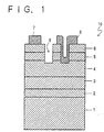
- FIG. 1 shows a LED 10 embodied in Example 1. It has a sapphire (Al 2 O 3 ) substrate 1 upon which the following five layers are consecutively formed: an AlN buffer layer 2; a silicon (Si) doped GaN n + -layer 3 of high carrier (n-type) concentration; a Si-doped (Al x2 Ga 1-x2 ) y2 In 1-y2 N n + -layer 4 of high carrier (n-type) concentration; a cadmium (Cd) and Si-doped (Al x1 Ga 1-x1 ) y1 In 1-y1 N emission layer 5; and Mg-doped (Al x2 Ga 1-x2 ) y2 In 1-y2 N p-layer 6.
- AlN buffer layer 2 a silicon (Si) doped GaN n + -layer 3 of high carrier (n-type) concentration
- the AlN layer 2 has 50nm thickness.
- the GaN n + -layer 3 is about 2.0 ⁇ m in thickness and has a 2 x 10 18 /cm 3 electron concentration.
- the n + -layer 4 is about 2.0 ⁇ m in thickness and has a 2 x 10 18 /cm 3 electron concentration.
- the emission layer 5 is about 0.5 ⁇ m in thickness.
- the i-layer 6 is about 1.0 ⁇ m in thickness and has a 2 x 10 17 /cm 3 hole concentration.
- Nickel electrodes 7 and 8 are connected to the p-layer 6 and the n + -layer 4, respectively. They are electrically insulated by a groove 9.
- the LED 10 is produced by gaseous phase growth, called metal organic vapor phase epitaxy referred to as MOVPE hereinafter.
- the gases employed in this process are ammonia (NH 3 ), a carrier gas (H 2 or N 2 ), trimethyl gallium (Ga(CH 3 ) 3 ) (TMG hereinafter), trimethyl aluminum (Al(CH 3 ) 3 ) (TMA hereinafter), trimethyl indium (In(CH 3 ) 3 ) (TMI hereinafter), dimethylcadmium ((Cd(CH 3 ) 2 ) (DMCd hereinafter), silane (SiH 4 ), diethylzinc ((C 2 H 5 ) 2 Zn) (DEZ hereinafter) and biscyclopentadienyl magnesium (Mg(C 5 H 5 ) 2 ) (CP 2 Mg hereinafter).
- the single crystalline sapphire substrate 1 whose main surface 'a' was cleaned by an organic washing solvent and heat treatment, was placed on a susceptor in a reaction chamber for the MOVPE treatment. Then the sapphire substrate 1 was etched at 1100 °C by a vapor of H 2 fed into the chamber at a flow rate of 2 liter/min. under normal pressure for a period of 5 min.
- a 50nm thick AlN buffer layer 2 was epitaxially formed on the surface 'a' under conditions of lowering the temperature in the chamber to 400 °C, keeping the temperature constant, and supplying H 2 , NH 3 and TMA for a period of about 90 sec. at a flow rate of 20 liter/min., 10 liter/min., and 1.8 x 10 -5 mol/min., respectively.
- the buffer layer 2 On the buffer layer 2, about a 2.2 ⁇ m thick Si-doped GaN n + -layer 3 of high carrier concentration with an electron concentration of about 2 x 10 18 /cm 3 was formed under conditions of keeping the temperature of the sapphire substrate 1 at 1150°C and supplying H 2 , NH 3 , TMG, and diluted silane to 0.86 ppm by H 2 for thirty minutes at a flow rate of 20 liter/min., 10 liter/min., 1.7 x 10 -4 mol/min. and 200 ml/min., respectively.
- the following manufacturing process provides for an emission layer 5 as an active layer, an n + -layer 4 of high carrier concentration, and a p-layer 6 as a clad layer; the LED 10 is designed to emit at a 450 nm wavelength peak in the luminous spectrum and have luminous centers of Cd and Si.
- n + -layer 3 On the n + -layer 3, about a 0.5 ⁇ m thick Si-doped (Al 0.47 Ga 0.53 ) 0.9 In 0.1 N n + -layer 4 of high carrier concentration with an electron concentration of 1 x 10 18 /cm 3 was formed under conditions of keeping the temperature of the sapphire substrate 1 at 850 °C and supplying N 2 or H 2 , NH 3 , TMG, TMA, TMI, and diluted silane to 0.86 ppm by H 2 for 60 min. at flow rate of 10 liter/min., 10 liter/min., 1.12 x 10 -4 mol/min., 0.47 x 10 -4 mol/min., 0.1 x 10 -4 mol/min. and 10 x 10 -9 mol/min., respectively.
- n + -layer 4 On the n + -layer 4, about a 0.5 ⁇ m thick Cd and Si-doped(Al 0.3 Ga 0.7 ) 0.94 In 0.06 N emission layer 5 was formed under conditions of keeping the temperature of the sapphire substrate 1 at 850 °C and supplying N 2 or H 2 , NH 3 , TMG, TMA, TMI, DMCd, and diluted silane to 0.86 ppm by H 2 for 60 min. at a flow rate of 20 liter/min., 10 liter/min., 1.53 x 10 -4 mol/min., 0.47 x 10 -4 mol/min., 0.02 x 10 -4 mol/min., 2 x 10 -7 mol/min.
- the layer 5 exhibited high resistivity.
- the impurity concentrations of the Cd and the Si doped to the emission layer 5 were 5 x 10 18 /cm 3 and 1 x 10 18 /cm 3 , respectively.
- Mg-doped (Al 0.47 Ga 0.53 ) 0.9 In 0.1 N p-layer 6 was formed under conditions of keeping the temperature of the sapphire substrate 1 at 1000 °C and supplying N 2 or H 2 , NH 3 , TMG, TMA, TMI, and CP 2 Mg for 120 min. at a flow rate of 20 liter/min., 10 liter/min., 1.12 x x 10 -4 mol/min., 0.47 x 10 -4 mol/min., 0.1 x 10 -4 mol/min. and 2 x 10 -4 mol/min., respectively.
- Resistivity of the p-layer 6 was 10 8 ⁇ cm or more exhibiting insulative characteristics.
- the impurity concentration of the Mg-doped into the p-layer 6 was 1 x 10 20 /cm 3 .
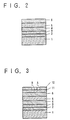
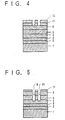
- FIGS. 3 to 7 show sectional views of an individual element on the wafer.
- a wafer with a large number of elements thereon is treated by the following process and divided or diced into individual elements.
- a 200 nm thick SiO 2 layer 11 was formed on the p-layer 6 by sputtering. Then, the layer 11 was coated with a photoresist layer 12.
- the part or area A is an electrode forming part which corresponds to a place where a hole 15, shown in FIG. 5, is formed extending to and into the n + -layer 4 of high carrier concentration.
- the part or area B corresponds to a place where a groove 9 shown in FIGS. 5 and 6 is formed for insulating or electrically insulating the part or area A from an electrode in contact with the p-layer 5.
- the SiO 2 layer 11 remaining on the p-layer 6 was removed by hydrofluoric acid as shown in FIG. 6.
- a nickel (Ni) layer 13 was laminated on the entire surface of the device by vapor deposition. Thus, the so-formed Ni layer 13 in the hole 15 is in electrical contact with the n + -layer 4 of high carrier concentration.
- a photoresist 14 was deposited on the Ni layer 13 and, then, was selectively etched off by photolithography as shown in FIG. 7 leaving patterns of configuration for electrodes connected to the n + -layer 4 of high carrier concentration and the p-layer 6, respectively.
- the exposed part or area of the Ni layer 13 from the photoresist 14 was etched off by an etching liquid such as nitric acid. At this time, the nickel layer 13 laminated in the groove 9 was also removed completely. Then, the photoresist layer 14 was removed by a photoresist removal liquid such as acetone. There were formed two electrodes, the electrode 8 for the n + -layer 4 of high carrier concentration and the electrode 7 for the p-layer 6. A wafer treated with the above-mentioned process was divided or diced into each element which shows a gallium nitride light-emitting diode with a p-n junction structure as shown in FIG. 1.
- the obtained LED 10 was found to have a luminous intensity of 100 mcd and a wavelength of 450 nm by driving current of 20 mA.
- the emission layer 5 preferably contains impurity concentrations of Cd and Si within a range of 1 x 10 17 /cm 3 to 1 x 10 20 /cm 3 , respectively, in order to improve luminous intensity. It is further desirable that the concentration of Si is smaller than that of Cd by ten to fifty percent.
- a double hetero-junction structure was utilized for the LED 10 in this embodiment.
- a single hetero-junction structure can be utilized.
- composition ratio of Al, Ga, and In in the respective three layers 4, 5, and 6 is selectively designed to meet the lattice constants of their layers 4, 5, and 6 with the lattice constant of GaN in the n + -layer 3 of high carrier concentration as precisely as possible.
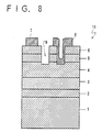
- FIG. 8 shows a LED 10 utilized in Example 2.
- the emission layer 5 in Example 1 was doped with Cd and Si.
- an emission layer 5 is doped with Zn and Si.
- n + -layer 4 of high carrier concentration with an electron concentration of 2 x 10 19 /cm 3 was formed on the n + -layer 3 under conditions of lowering the temperature in the chamber to 800 °C, keeping the temperature constant, and supplying N 2 , NH 3 , TMG, TMA, TMI, and diluted silane to 0.86 ppm by H 2 for 120 min.
- N emission layer 5 was formed on the n + -layer 4 under conditions of lowering the temperature in the chamber to 1150 °C, keeping it constant, and supplying N 2 , NH 3 , TMG, TMA, TMI, diluted silane to 0.86 ppm by H 2 , and DEZ for 7 min. at a flow rate of 20 liter/min., 10 liter/min., 1.53 x 10 -4 mol/min., 0.47 x 10 -4 mol/min., 0.02 x 10 -4 mol/min.
- the impurity concentration of the Zn- and Si-doped into the emission layer 5 was 2 x 10 18 /cm 3 and 1 x 10 18 /cm 3 , respectively.
- N p-layer 6 was formed on the emission layer 5 under conditions of lowering the temperature in the chamber to 1100 °C, keeping the temperature constant, and supplying N 2 , NH 3 , TMG, TMA, TMI, and CP 2 Mg at a flow rate of 20 liter/min., 10 liter/min., 1.12 x 10 -4 mol/min., 0.47 x 10 -4 mol/min., 0.1 x 10 -4 mol/min., and 2 x 10 -4 mol/min., respectively.
- the impurity concentration of Mg doped into the p-layer 6 was 1 x 10 20 /cm 3 . At this stage, the p-layer 6 remained insulative with a resistivity of 10 8 ⁇ cm or more.
- the p-layer 6 was processed to have p-type conduction by electron beam irradiation under the same conditions described in Example 1.
- the subsequent process steps of forming the electrodes are the same as that described in the previous example.
- the so-obtained LED 10 was found to have a luminous intensity of 1000 mcd and a wavelength of 450 nm by driving current of 20 mA.
- FIG. 9 shows a structural view of a LED 10 embodied in Example 3.
- the LED 10 in Example 3 was manufactured by additionally doping Mg to the emission layer 5 of the LED in Example 2.
- Other layers and electrodes were manufactured in the same way as those in Example 2.
- CP 2 Mg was fed at a flow rate of 2 x 10 -4 mol/min. into a chamber in addition to the gasses employed in Example 2 in order to manufacture the emission layer 5 in Example 3.
- the emission layer 5 was about 0.5 ⁇ m thick comprising Mg, Zn, and Si-doped (Al 0.09 Ga 0.91 ) 0.99 In 0.01 N. Its resistivity was 10 8 ⁇ cm remaining insulative. Impurity concentration of Mg, Zn, and Si was 1 x 10 19 /cm 3 , 2 x 10 18 /cm 3 , and 1 x 10 18 /cm 3 , respectively.
- both of the emission layer 5 and a p-layer 6 were subject to electron beam irradiation with the electron beam diffraction device under as same conditions as in Example 1.
- the emission layer 5 and the p-layer 6 turned into layers exhibiting p-type conduction with a hole concentration of 2 x 10 17 /cm 3 and resistivity of 2 ⁇ cm.
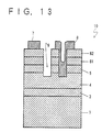
- FIG. 10 shows a structural view of a LED 10 embodied in Example 4.
- an emission layer 5 includes GaN and had a single hetero-junction structure. Namely, one junction comprises a heavily Si-doped n + -layer 4 of high carrier concentration and a Zn- and Si-doped GaN emission layer 5, and another junction includes the GaN emission layer 5 and a Mg-doped Al 0.1 Ga 0.9 N p-layer 61 with p-type conduction.
- the Mg-doped GaN p-layer 62 as a contact layer is formed on the p-layer 61.
- An insulation groove 9 is formed through the contact layer 62, the p-layer 61 and the emission layer 5.
- the LED 10 in this example has a sapphire substrate 1 upon which the following five layers are consecutively formed: an AlN buffer layer 2; a Si-doped GaN n + -layer 4 of high carrier (n-type) concentration; a Zn and Si-doped GaN emission layer 5, Mg-doped Al 0.1 Ga 0.9 N p-layer 61, and Mg-doped GaN contact layer 62.
- the AlN layer 2 has a 50 nm thickness.
- the GaN n + -layer 4 has about a 4.0 ⁇ m thickness and a 2 x 10 18 /cm 3 electron concentration.
- the emission layer 5 has about a 0.5 ⁇ m thickness.
- the p-layer 61 has about a 0.5 ⁇ m thickness and a 2 x 10 17 /cm 3 hole concentration.
- the contact layer 62 has about a 0.5 ⁇ m thickness and a 2 x 10 17 /cm 3 hole concentration.
- Nickel electrodes 7 and 8 are formed to connect to the contact layer 62 and the n + -layer 4 of high carrier concentration, respectively The two electrodes are electrically insulated by a groove 9.
- the sapphire substrate 1 and the AlN buffer layer 2 were prepared by the same process described in detail in Example 1.
- the following manufacturing process and composition ratio provide for the three layers, the emission layer 5 as an active layer, the p-layer 62 as a clad layer, and the contact layer 62.
- the LED is designed to have 430 nm wavelength at peak in the luminous spectrum and have luminous centers of Zn and Si.
- n + -layer 4 About a 0.5 ⁇ m thick Zn- and Si-doped GaN emission layer 5 was formed on the n + -layer 4 under conditions of lowering the temperature in the chamber to 1000 °C, keeping it constant and supplying N 2 or H 2 . NH 3 . TMG. DMZ, and diluted silane to 0.86 ppm by H 2 for 8 min. at a flow rate of 20 liter/min., 10 liter/min., 1.53 x 10 -4 mol/min., 2 x 10 -7 mol/min., and 10 x 10 -9 mol/min., respectively.
- Mg-doped Al 0.1 Ga 0.9 N p-layer 61 was formed on the emission layer 5 under conditions of lowering the temperature in the chamber to 1000 C, keeping the temperature constant and supplying N 2 or H 2 , NH 3 , TMG, TMA, and CP 2 Mg for 7 min. at a flow rate of 20 liter/min., 10 liter/min., 1.12 x 10 -4 mol/min., 0.47 x 10 -4 mol/min., and 2 x 10 -7 mol/min., respectively.
- the p-layer 61 remained insulative with a resistivity of 10 8 ⁇ cm or more.
- the impurity concentration of the Mg-doped into the p-layer 61 was 1 x 10 19 /cm 3 .
- Mg-doped GaN contact layer 62 was formed on the p-layer 61 under conditions of,lowering the temperature in the chamber to 1000 °C, keeping'the temperature constant and supplying N 2 or H 2 , NH 3 , TMG, and CP 2 Mg for 10 min. at a flow rate of 20 liter/min., 10 liter/min., 1.12 x 10 -4 mol/min., and 2 x 10 -4 mol/min., respectively.
- the Mg-doped contact layer 62 remained insulative with a resistivity of 10 8 ⁇ cm or more.
- the impurity concentration of the Mg-doped into the contact layer 62 was 1 x 10 20 /cm 3 .
- the p-layer 61 and contact layer 62 were uniformly irradiated by an electron beam under the same conditions as described in Example 1. Consequently, the p-layer 61 and contact layer 62 are processed to exhibit p-type conduction with a 2 x 10 17 /cm 3 hole concentration and 2 ⁇ cm or more resistivity.
- the subsequent process steps of forming the electrodes is the same as that described in the previous example.
- the LED 10 having a single hetero-junction structure is obtained whose emission layer is doped with Zn as an acceptor and Si as a donor impurity.
- doping Mg and irradiating electrons into the emission layer 5 can be used to obtain an emission layer 5 with p-type conduction.
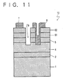
- FIG. 11 shows a LED 10 embodied in this example.
- Three layers, a p-layer 61, an emission layer 5, and an n + -layer 4, are unique to Example 5.
- the p-layer 61 is formed of Mg-doped Al x1 Ga 1-x1 N.
- the emission layer 5 is Zn- and Si-doped Al x2 Ga 1-x2 N.
- the n + -layer 4 of high carrier concentration is Si-doped Al x3 Ga 1-x3 N.
- Other layers and electrodes are formed the same as those described in Example 4.
- the composition ratio of X1, X2 and x3 in each layer is designed to make the band gap of the emission layer 5 smaller than those of the n - -layer 4 and p-layer 61 forming a double hetero-junction structure or a single hetero-junction structure. Thanks to this structure, carriers are confined in the emission layer 5 contributing to higher luminous intensity.
- the emission layer 5 can exhibit any one of semi-insulative, p-type conductivity, or n-type conductivity.
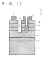
- FIG. 12 shows a LED 10 embodied in this example.
- Three layers, a p-layer 61, an emission layer 5, and an n + -layer 4, are unique to Example 6.
- the p-layer 61 formed of Mg-doped Al x1 Ga 1-x1 N.
- the emission layer 5 is formed of Zn- and Si-doped Ga y In 1-y N.
- the n + -layer 4 of high carrier concentration is formed of Si-doped Al x2 Ga 1-x2 N.
- Other layers and electrodes are formed the same as those described in Example 4.
- the composition ratio of x1, x2, and x3 in each layer is designed to make the band gap of the emission layer 5 smaller than those of the n + -layer 4 and p-layer 61 forming a double hetero-junction structure or a single hetero-junction structure. Thanks to this structure, carriers are confined in the emission layer 5 contributing to higher luminous intensity.
- the emission layer 5 can exhibit any one of semi-insulative, p-type conductivity, or n-type conductivity.
- the LED 10 in this example has a sapphire substrate 1 which has the following five layers are consecutively formed thereon: an AlN buffer layer 2; a Si-doped Al x2 Ga 1-x2 N n + -layer 4 of high carrier (n-type) concentration; a Zn- and Si-doped Ga 0.94 In 0.06 N emission layer 5, Mg-doped Al 0.1 Ga 0.9 N p-layer 61 of p-type, and an Mg-doped GaN contact layer 62 of p-type.
- the AlN layer 2 has a 500 ⁇ thickness.
- the Al x2 Ga 1-x2 N n + -layer 4 has about a 4.0 ⁇ m thickness and a 2 x 10 18 /cm 3 electron concentration.
- the emission layer 5 has about 0.5 ⁇ m thickness.
- the p-layer 61 has about a 0.5 ⁇ m thickness and a 2 x 10 17 /cm 3 hole concentration.
- the contact layer 62 has about a 0.5 ⁇ m thickness and a 2 x 10 17 /cm 3 hole concentration.
- Nickel electrodes 7 and 8 are formed to connect to the contact layer 62 and n + -layer 4 of high carrier concentration, respectively. The two electrodes are electrically insulated by a groove 9.
- a manufacturing process for the LED 10 of FIG. 12 is as follows.
- the sapphire substrate 1 and the AlN buffer layer 2 were prepared by the same process described in detail in Example 1.
- On the AlN buffer layer 2. about a 4.0 ⁇ m thick Si-doped Al x2 Ga 1-x2 N n - - layer 4 of high carrier concentration with an electron concentration of 2 x 10 18 /cm 3 was formed under conditions of lowering the temperature in the chamber to 1150 °C, keeping it constant, and supplying N 2 , NH 3 , TMG, TMA, and diluted silane to 0.86 ppm by H 2 for 60 min. at a flow rate of 20 liter/min., 10 liter/min., 1.12 x 10 -4 mol/min., 0.47 x 10 -4 mol/min., and 10 x 10 -9 mol/min., respectively.
- the emission layer 5 as an active layer
- the p-layer 61 as a clad layer
- the contact layer 62 we show an example where the LED 10 is designed to have 450 nm wavelength at peak in luminous spectrum and have luminous centers of Zn and Si.
- n + -layer 4 About a 0.5 ⁇ m thick Zn- and Si-doped Ga 0.94 In 0.06 N emission layer 5 was formed on the n + -layer 4 under conditions of raising the temperature in the chamber to 850 °C, keeping it constant, and supplying N 2 or H 2 , NH 3 , TMG, TMI, DMZ and, silane for 60 min. at a flow rate of 20 liter/min., 10 liter/min., 1.53 x 10 -4 mol/min., 0.02 x 10 -4 mol/min., 2 x 10 -7 mol/min., and 10 x 10 -9 mol/min., respectively.
- Mg-doped Al 0.1 Ga 0.9 N p-layer 61 was formed on the emission layer 5 under conditions of raising the temperature in the chamber to 1000 °C. keeping the temperature constant and supplying N 2 or H 2 , NH 3 , TMG, TMA, and CP 2 Mg for 7 min. at a flow rate of 20 liter/min., 10 liter/min., 1.12 x 10 -4 mol/min., 0.47 x 10 -4 mol/min., and 2 x 10 -7 mol/min., respectively.
- the p-layer 61 remained insulative with a resistivity of 10 8 ⁇ cm or more.
- the impurity concentration of the Mg doped into the p-layer 61 was 1 x 10 19 /cm 3 .
- Mg-doped GaN contact layer 62 was formed on the p-layer 61 under conditions of keeping the temperature in the chamber at 1000 °C and supplying N 2 or H 2 , NH 3 , TMG, and CP 2 Mg for 10 min. at a flow rate of 20 liter/min., 10 liter/min., 1.12 x 10 -4 mol/min., and 2 x 10 -4 mol/min., respectively.
- the Mg-doped contact layer 62 remained insulative with a resistivity of 10 8 ⁇ cm or more.
- the impurity concentration of the Mg doped into the contact layer 62 was 1 x 10 20 /cm 3 .
- the p-layer 61 and contact layer 62 were uniformly irradiated by an electron beam with the same conditions described in Example 1. Consequently, the p-layer 61 and contact layer 62 are processed to exhibit p-type conduction with a 2 x 10 17 /cm 3 hole concentration and a 2 ⁇ cm resistivity.
- the subsequent process steps of forming the electrodes is the same as that described in the previous example.
- the emission layer 5 can exhibit any one of semi-insulation, p-type conductivity, or n-type conductivity.
- concentration of the Zn-doped to the emission layer 5 is higher than that of the Si, the layer 5 exhibits semi-insulative characteristics.
- concentration of the Zn is smaller than that of the Si, the emission layer 5 exhibits n-type conduction.
- the impurity concentration of Zn and Si doped to the emission layer 5 is preferably in the 1 x 10 17 /cm 3 to 1 x 10 20 /cm 3 range, respectively.
- the concentration is more preferably in the 1 x 10 18 /cm 3 to 1 x 10 19 /cm 3 range.
- the impurity concentration be lower than 1 x 10 18 /cm 3 , because the luminous intensity of the LED decreases as a result.
- the impurity concentration is higher than 1 x 10 19 /cm 3 , because poor crystallinity occurs.
- the concentration of Si is ten to one-tenth as that of Zn. The most preferable concentration of Si is in the one to one-tenth range or closer to one-tenth to Zn.
- Cd, Zn, and Mg were employed as acceptor impurities and Si as a donor impurity.
- beryllium (Be) and mercury (Hg) can be used as an acceptor impurity.
- carbon (C), germanium (Ge), tin (Sn), lead (Pb), sulfur (S), selenium (Se), and tellurium (Te) can be used as a donor impurity.
- Electron irradiation was used in Examples 1 to 6 in order to process an emission layer 5 to exhibit p-type conduction.
- annealing, heat processing in the atmosphere of N 2 plasma gas and laser irradiation can be used.
- FIG. 14 shows a structural view of a LED 10 embodied in Example 7.
- the LED 10 in this example was manufactured by additionally doping Mg to the emission layer 5 of the LED 10 in Example 1.
- Other layers and electrodes were manufactured the same way as those described in Example 1.
- CP 2 Mg was fed at a flow rate of 2 x 10 -7 mol/min. into a chamber in addition to gasses employed in Example 1 in order to manufacture the emission layer 5 in Example 7.
- the emission layer 5 was about a 0.5 ⁇ m thick including Mg-, Cd-, and Si-doped (Al 0.09 Ga 0.91 ) 0.99 In 0.01 N remaining high insulative.
- Impurity concentration of the Mg, Cd and Si was 1 x 10 20 /cm 3 , 5 x 10 18 /cm 3 , and 1 x 10 18 /cm 3 , respectively.
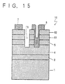
- FIGS. 15 and 16 show structural views of a LED 10 embodied in Example 8.
- the LED 10 in this example was manufactured by additionally doping Mg and irradiating -electrons into the emission layer 5 of the LED 10 in Example 6.
- the emission layer 5 of Example 8 includes Mg-, Zn-, and Si-doped Ga y In 1-y N exhibiting p-type conduction.
- Other layers and electrodes were manufactured the same way as those described in Example 1.
- FIG. 16 shows an example where the LED 10 is designed to have a 450 nm wavelength at peak in the luminous intensity.
- the manufacturing process and composition equation of the three layers, the emission layer 5 as an active layer, the p-layer 61 as a clad layer and the contact layer 62 are described hereinafter.
- the CP 2 Mg was fed at a flow rate of 2 x 10 -4 mol/min. into a chamber in addition to gasses employed in Example 6 in order to manufacture the emission layer 5 in Example 8.
- the emission layer 5 was about a 0.5 ⁇ m thick including Mg-, Zn-, and Si-doped Ga 0.94 In 0.06 N remaining highly insulative.
- the emission layer 5, p-layer 61 and contact layer 61 were uniformly irradiated by an electron diffraction device under the same conditions as those described in Example 1. This irradiation changed the emission layer 5, p-layer 61, and contact layer 62 into layers exhibiting p-type conduction with a hole concentration of 2 x 10 17 /cm 3 and a resistivity of 2 ⁇ cm.
- the impurity concentration of Zn and Si doped into the emission layer 5 are preferably in the 1 x 10 17 /cm 3 to 1 x 20 20 /cm 3 range, respectively.
- the concentration is more preferably in the 1 x 10 18 /cm 3 to 1 x 10 19 /cm 3 range.
- the impurity concentration be lower than 1 x 10 18 /cm 3 , because luminous intensity of the LED decreases as a result.
- the impurity concentration be higher than 1 x 10 19 /cm 3 , because poor crystallinity occurs.
- the concentration of Si be ten to one-tenth as same as that of Zn. The most preferable concentration of Si is in the two to one-tenth range.
- Cd, Zn and Mg were employed as acceptor impurities and Si as a donor impurity.
- beryllium (Be) and mercury (Hg) can be used as an acceptor impurity.
- carbon (C), germanium (Ge), tin (Sn), lead (Pb), sulfur (S), selenium (Se) and tellurium (Te) can be used as a donor impurity.
- Electron irradiation was used in Examples 7 and 8 in order to change layers to have p-type conduction.
- annealing heat process in the atmosphere of N 2 plasma gas, laser irradiation and any combination thereof can be used.
Landscapes
- Led Devices (AREA)
Claims (11)
- Lichtemittierende Halbleitervorrichtung (10) aus einer Stickstoffverbindung der Gruppe III, die die Formel AlxGayIn1-x-yN erfüllt, wobei 0 ≤ x ≤ 1, 0 ≤ y ≤ 1 und 0 ≤ x+y ≤ 1 ist, die folgendes umfasst:eine n-Schicht (4) vom n-Leitungstyp;eine Emissionsschicht (5) die auf der n-Schicht gebildet ist;eine p-Schicht (6, 61) vom p-Leitungstyp, die auf der Emissionsschicht gebildet ist;eine Nickel(Ni)-Elektrode (7), die mit der p-Schicht (6) in Kontakt steht; undwobei die Emissionsschicht (5) mit einem Akzeptor und Donorfremdatomen dotiert ist, und eine Übergangszone zwischen der n-Schicht (4) und der Emissionsschicht (5) und eine Übergangszone zwischen der Emissionsschicht (5) und der p-Schicht (6, 61) jeweils eine Heteroübergangszonenstruktur bildet.
- Lichtemittierende Halbleitervorrichtung gemäß Anspruch 1, wobei die Vorrichtung weiter eine Kontaktschicht (62) vom p-Leitungstyp und aus Galliumnitrid (GaN) umfasst, die zwischen der p-Schicht und der Nickel (Ni)- Elektrode gebildet ist.
- Lichtemittierende Halbleitervorrichtung gemäß Anspruch 1, wobeidie n-Schicht (4) aus einer Verbindung ist, die die Formel Alx3Ga1-x3N erfüllt, wobei 0 ≤ x3 < 1;die Emissionsschicht (5) aus einer Stickstoffverbindung der Gruppe III ist, die die Formel Gax1In1-x1N erfüllt, wobei 0 < x1 ≤ 1;die p-Schicht (6, 61) aus Aluminiumgalliumnitrid ist, das die Formel Alx2Ga1-x2N erfüllt, wobei 0 < x2 < 1 ist; undzwischen der p-Schicht und der Ni-Elektrode eine Kontaktschicht (62) vom p-Leitungstyp und aus Galliumnitrid (GaN) gebildet ist.
- Lichtemittierende Halbleitervorrichtung gemäß Anspruch 1, wobeidie n-Schicht (4) aus einer Verbindung ist, die die Formel Alx3Ga1-x3N erfüllt, wobei 0 ≤ x3 < 1;die Emissionsschicht (5) aus einer Stickstoffverbindung der Gruppe III ist, die die Formel Gax1In1-x1N erfüllt, wobei 0 < x1 ≤ 1 ist, und die mit Silizium (Si) und Zink (Zn) dotiert ist; und die p-Schicht (6, 61) aus Aluminiumgalliumnitrid ist, das die Formel Alx2Ga1-x2N erfüllt, wobei 0 < x2 < 1 ist.
- Lichtemittierende Halbleitervorrichtung gemäß Anspruch 4, wobei die Vorrichtung weiter eine Kontaktschicht (62) vom p-Leitungstyp umfasst, die zwischen der p-Schicht (61) und der Nickelelektrode (7) gebildet ist, wobei die Kontaktschicht (62) eine schmalere Bandlücke besitzt als die p-Schicht (61).
- Lichtemittierende Halbleitervorrichtung gemäß Anspruch 5, wobei die Kontaktschicht (62) aus Galliumnitrid (GaN) hergestellt ist.
- Lichtemittierende Halbleitervorrichtung gemäß Anspruch 4, wobei die Konzentration an Silizium (Si), mit dem die Emissionsschicht (5) dotiert ist, in dem Bereich von 1 x 1017 cm-3 bis 1 x 1020 cm-3 liegt.
- Lichtemittierende Halbleitervorrichtung gemäß Anspruch 4, wobei die Konzentration an Zink (Zn), mit dem die Emissionsschicht (5) dotiert ist, in dem Bereich von 1 x 1017 cm-3 bis 1 x 1020 cm-3 liegt.
- Lichtemittierende Halbleitervorrichtung aus einer Stickstoffverbindung der Gruppe III, die eine n-Schicht, eine Emissionsschicht und eine wie in Anspruch 1 definierte p-Schicht, umfasst,
wobei die Emissionsschicht eine Verbindung aus einer Aluminiumverbindung, die die Formel Alx4Gay4In1-x4-y4N erfüllt, wobei 0 < x4 ≤ 1, 0 ≤ y4 ≤ 1 und 0 ≤ x4+y4 ≤ 1, und aus Galliumnitrid (GaN) umfasst, und mit einem Akzeptor und Donorfremdatomen dotiert ist, und eine Übergangszone zwischen der n-Schicht (4) und der Emissionsschicht (5) und eine Übergangszone zwischen der Emissionsschicht (5) und der p-Schicht (6) jeweils eine Heteroübergangszonenstruktur bildet. - Lichtemittierende Halbleitervorrichtung gemäß Anspruch 9, wobei die Vorrichtung weiter eine Nickel (Ni)- Elektrode (7) umfasst, die mit der p-Schicht (6) in Kontakt steht.
- Lichtemittierende Halbleitervorrichtung gemäß Anspruch 10, wobei die Vorrichtung weiter eine Kontaktschicht (62) vom p-Leitungstyp und aus Galliumnitrid (GaN) umfasst, die zwischen der p-Schicht (61) und der Nickel (Ni)-Elektrode (7) gebildet ist.
Priority Applications (1)
| Application Number | Priority Date | Filing Date | Title |
|---|---|---|---|
| EP99101801A EP0911888B1 (de) | 1994-03-22 | 1995-03-21 | Lichtemittierende Halbleitervorrichtung, die eine Stickstoff enthaltende Verbindung der Gruppe III verwendet |
Applications Claiming Priority (9)
| Application Number | Priority Date | Filing Date | Title |
|---|---|---|---|
| JP7651494 | 1994-03-22 | ||
| JP76514/94 | 1994-03-22 | ||
| JP7651494 | 1994-03-22 | ||
| JP11348494 | 1994-04-28 | ||
| JP11348494A JP3016241B2 (ja) | 1994-03-22 | 1994-04-28 | 3族窒化物半導体発光素子 |
| JP113484/94 | 1994-04-28 | ||
| JP19791494A JP3307094B2 (ja) | 1994-07-28 | 1994-07-28 | 3族窒化物半導体発光素子 |
| JP197914/94 | 1994-07-28 | ||
| JP19791494 | 1994-07-28 |
Related Child Applications (1)
| Application Number | Title | Priority Date | Filing Date |
|---|---|---|---|
| EP99101801A Division EP0911888B1 (de) | 1994-03-22 | 1995-03-21 | Lichtemittierende Halbleitervorrichtung, die eine Stickstoff enthaltende Verbindung der Gruppe III verwendet |
Publications (2)
| Publication Number | Publication Date |
|---|---|
| EP0675552A1 EP0675552A1 (de) | 1995-10-04 |
| EP0675552B1 true EP0675552B1 (de) | 2001-08-08 |
Family
ID=27302178
Family Applications (2)
| Application Number | Title | Priority Date | Filing Date |
|---|---|---|---|
| EP99101801A Expired - Lifetime EP0911888B1 (de) | 1994-03-22 | 1995-03-21 | Lichtemittierende Halbleitervorrichtung, die eine Stickstoff enthaltende Verbindung der Gruppe III verwendet |
| EP95104140A Expired - Lifetime EP0675552B1 (de) | 1994-03-22 | 1995-03-21 | Lichtemittierende Halbleitervorrichtung mit Verbindung aus Stickstoff und Elementen der Gruppe III |
Family Applications Before (1)
| Application Number | Title | Priority Date | Filing Date |
|---|---|---|---|
| EP99101801A Expired - Lifetime EP0911888B1 (de) | 1994-03-22 | 1995-03-21 | Lichtemittierende Halbleitervorrichtung, die eine Stickstoff enthaltende Verbindung der Gruppe III verwendet |
Country Status (2)
| Country | Link |
|---|---|
| EP (2) | EP0911888B1 (de) |
| DE (2) | DE69534387T2 (de) |
Families Citing this family (9)
| Publication number | Priority date | Publication date | Assignee | Title |
|---|---|---|---|---|
| JP2666237B2 (ja) * | 1994-09-20 | 1997-10-22 | 豊田合成株式会社 | 3族窒化物半導体発光素子 |
| US5739554A (en) * | 1995-05-08 | 1998-04-14 | Cree Research, Inc. | Double heterojunction light emitting diode with gallium nitride active layer |
| EP0772249B1 (de) * | 1995-11-06 | 2006-05-03 | Nichia Corporation | Halbleitervorrichtung aus einer Nitridverbindung |
| TW425722B (en) * | 1995-11-27 | 2001-03-11 | Sumitomo Chemical Co | Group III-V compound semiconductor and light-emitting device |
| JPH1065215A (ja) * | 1996-08-22 | 1998-03-06 | Toyoda Gosei Co Ltd | Iii族窒化物半導体発光素子 |
| US8558960B2 (en) | 2010-09-13 | 2013-10-15 | Semiconductor Energy Laboratory Co., Ltd. | Liquid crystal display device and method for manufacturing the same |
| CN106486572B (zh) * | 2015-09-02 | 2020-04-28 | 新世纪光电股份有限公司 | 发光二极管芯片 |
| US10134950B2 (en) | 2016-08-18 | 2018-11-20 | Genesis Photonics Inc. | Micro light emitting diode and manufacturing method thereof |
| TWD191816S (zh) | 2017-12-12 | 2018-07-21 | 新世紀光電股份有限公司 | 發光二極體晶片 |
Citations (2)
| Publication number | Priority date | Publication date | Assignee | Title |
|---|---|---|---|---|
| EP0607435A1 (de) * | 1992-08-07 | 1994-07-27 | Asahi Kasei Kogyo Kabushiki Kaisha | Halbleiteranordnung auf nitridbasis und verfahren zu ihrer herstellung |
| EP0622858A2 (de) * | 1993-04-28 | 1994-11-02 | Nichia Chemical Industries, Ltd. | Halbleitervorrichtung der III-V Verbindung auf Basis einer Galliumnitrid-Halbleiterverbindung und Verfahren zu ihrer Herstellung |
Family Cites Families (3)
| Publication number | Priority date | Publication date | Assignee | Title |
|---|---|---|---|---|
| JP2778349B2 (ja) * | 1992-04-10 | 1998-07-23 | 日亜化学工業株式会社 | 窒化ガリウム系化合物半導体の電極 |
| US5578839A (en) * | 1992-11-20 | 1996-11-26 | Nichia Chemical Industries, Ltd. | Light-emitting gallium nitride-based compound semiconductor device |
| JP2914065B2 (ja) * | 1992-12-08 | 1999-06-28 | 日亜化学工業株式会社 | 青色発光素子及びその製造方法 |
-
1995
- 1995-03-21 DE DE69534387T patent/DE69534387T2/de not_active Expired - Fee Related
- 1995-03-21 EP EP99101801A patent/EP0911888B1/de not_active Expired - Lifetime
- 1995-03-21 DE DE69522026T patent/DE69522026T2/de not_active Expired - Fee Related
- 1995-03-21 EP EP95104140A patent/EP0675552B1/de not_active Expired - Lifetime
Patent Citations (2)
| Publication number | Priority date | Publication date | Assignee | Title |
|---|---|---|---|---|
| EP0607435A1 (de) * | 1992-08-07 | 1994-07-27 | Asahi Kasei Kogyo Kabushiki Kaisha | Halbleiteranordnung auf nitridbasis und verfahren zu ihrer herstellung |
| EP0622858A2 (de) * | 1993-04-28 | 1994-11-02 | Nichia Chemical Industries, Ltd. | Halbleitervorrichtung der III-V Verbindung auf Basis einer Galliumnitrid-Halbleiterverbindung und Verfahren zu ihrer Herstellung |
Non-Patent Citations (1)
| Title |
|---|
| B. GOLDENBERG ET AL.: "Ultraviolet and violet light-emitting GaN diodes grown by low-pressure metalorganic chemical vapor deposition", APPLIED PHYSICS LETTERS, vol. 62, no. 4, 25 January 1993 (1993-01-25), NEW YORK, US, pages 381 - 383, XP000335998, DOI: doi:10.1063/1.108963 * |
Also Published As
| Publication number | Publication date |
|---|---|
| EP0675552A1 (de) | 1995-10-04 |
| DE69522026D1 (de) | 2001-09-13 |
| DE69534387D1 (de) | 2005-09-22 |
| EP0911888A2 (de) | 1999-04-28 |
| EP0911888A3 (de) | 1999-06-23 |
| DE69534387T2 (de) | 2006-06-14 |
| EP0911888B1 (de) | 2005-08-17 |
| DE69522026T2 (de) | 2002-05-29 |
Similar Documents
| Publication | Publication Date | Title |
|---|---|---|
| US7332366B2 (en) | Light-emitting semiconductor device using group III nitrogen compound | |
| EP0703631B1 (de) | Lichtemittierende Vorrichtung aus einer Nitridverbindung der Gruppe III | |
| US5959401A (en) | Light-emitting semiconductor device using group III nitride compound | |
| US5945689A (en) | Light-emitting semiconductor device using group III nitride compound | |
| US5650641A (en) | Semiconductor device having group III nitride compound and enabling control of emission color, and flat display comprising such device | |
| US5700713A (en) | Light emitting semiconductor device using group III nitride compound and method of producing the same | |
| JP3654738B2 (ja) | 3族窒化物半導体発光素子 | |
| JPH0832112A (ja) | 3族窒化物半導体発光素子 | |
| EP0675552B1 (de) | Lichtemittierende Halbleitervorrichtung mit Verbindung aus Stickstoff und Elementen der Gruppe III | |
| JP3016241B2 (ja) | 3族窒化物半導体発光素子 | |
| JP3307094B2 (ja) | 3族窒化物半導体発光素子 | |
| US7045829B2 (en) | Light-emitting semiconductor device using Group III nitride compound | |
| JP3494841B2 (ja) | 3族窒化物半導体発光素子 | |
| JPH07297447A (ja) | 3族窒化物半導体発光素子 | |
| JP3341484B2 (ja) | 3族窒化物半導体発光素子 | |
| KR100246273B1 (ko) | 3족 니트라이드 화합물 반도체 발광 장치 | |
| JPH08125223A (ja) | 3族窒化物半導体発光素子及びその製造方法 | |
| JP2002289916A (ja) | 3族窒化物半導体発光素子 |
Legal Events
| Date | Code | Title | Description |
|---|---|---|---|
| PUAI | Public reference made under article 153(3) epc to a published international application that has entered the european phase |
Free format text: ORIGINAL CODE: 0009012 |
|
| 17P | Request for examination filed |
Effective date: 19950321 |
|
| AK | Designated contracting states |
Kind code of ref document: A1 Designated state(s): DE FR GB |
|
| 17Q | First examination report despatched |
Effective date: 19961210 |
|
| GRAG | Despatch of communication of intention to grant |
Free format text: ORIGINAL CODE: EPIDOS AGRA |
|
| GRAG | Despatch of communication of intention to grant |
Free format text: ORIGINAL CODE: EPIDOS AGRA |
|
| GRAH | Despatch of communication of intention to grant a patent |
Free format text: ORIGINAL CODE: EPIDOS IGRA |
|
| GRAH | Despatch of communication of intention to grant a patent |
Free format text: ORIGINAL CODE: EPIDOS IGRA |
|
| GRAA | (expected) grant |
Free format text: ORIGINAL CODE: 0009210 |
|
| AK | Designated contracting states |
Kind code of ref document: B1 Designated state(s): DE FR GB |
|
| REF | Corresponds to: |
Ref document number: 69522026 Country of ref document: DE Date of ref document: 20010913 |
|
| REG | Reference to a national code |
Ref country code: GB Ref legal event code: IF02 |
|
| ET | Fr: translation filed | ||
| PLBE | No opposition filed within time limit |
Free format text: ORIGINAL CODE: 0009261 |
|
| STAA | Information on the status of an ep patent application or granted ep patent |
Free format text: STATUS: NO OPPOSITION FILED WITHIN TIME LIMIT |
|
| 26N | No opposition filed | ||
| REG | Reference to a national code |
Ref country code: GB Ref legal event code: 746 Effective date: 20080204 |
|
| PGFP | Annual fee paid to national office [announced via postgrant information from national office to epo] |
Ref country code: GB Payment date: 20080326 Year of fee payment: 14 |
|
| PGFP | Annual fee paid to national office [announced via postgrant information from national office to epo] |
Ref country code: FR Payment date: 20080311 Year of fee payment: 14 Ref country code: DE Payment date: 20080313 Year of fee payment: 14 |
|
| GBPC | Gb: european patent ceased through non-payment of renewal fee |
Effective date: 20090321 |
|
| REG | Reference to a national code |
Ref country code: FR Ref legal event code: ST Effective date: 20091130 |
|
| PG25 | Lapsed in a contracting state [announced via postgrant information from national office to epo] |
Ref country code: DE Free format text: LAPSE BECAUSE OF NON-PAYMENT OF DUE FEES Effective date: 20091001 |
|
| PG25 | Lapsed in a contracting state [announced via postgrant information from national office to epo] |
Ref country code: GB Free format text: LAPSE BECAUSE OF NON-PAYMENT OF DUE FEES Effective date: 20090321 Ref country code: FR Free format text: LAPSE BECAUSE OF NON-PAYMENT OF DUE FEES Effective date: 20091123 |