EP0669705A2 - Leistungswandlungssystem - Google Patents
Leistungswandlungssystem Download PDFInfo
- Publication number
- EP0669705A2 EP0669705A2 EP95301247A EP95301247A EP0669705A2 EP 0669705 A2 EP0669705 A2 EP 0669705A2 EP 95301247 A EP95301247 A EP 95301247A EP 95301247 A EP95301247 A EP 95301247A EP 0669705 A2 EP0669705 A2 EP 0669705A2
- Authority
- EP
- European Patent Office
- Prior art keywords
- phase
- currents
- current
- conduction
- unit converters
- Prior art date
- Legal status (The legal status is an assumption and is not a legal conclusion. Google has not performed a legal analysis and makes no representation as to the accuracy of the status listed.)
- Granted
Links
- 238000006243 chemical reaction Methods 0.000 title claims abstract description 23
- 230000008859 change Effects 0.000 claims abstract description 6
- 238000001514 detection method Methods 0.000 claims description 26
- 238000010586 diagram Methods 0.000 description 15
- 101000956004 Homo sapiens Vitamin D-binding protein Proteins 0.000 description 2
- 102100038611 Vitamin D-binding protein Human genes 0.000 description 2
- 239000003990 capacitor Substances 0.000 description 2
- 230000003247 decreasing effect Effects 0.000 description 2
- 238000000034 method Methods 0.000 description 2
- 230000008569 process Effects 0.000 description 2
- 230000009471 action Effects 0.000 description 1
- 238000010276 construction Methods 0.000 description 1
- 238000009499 grossing Methods 0.000 description 1
- 230000004048 modification Effects 0.000 description 1
- 238000012986 modification Methods 0.000 description 1
Images


Classifications
-
- H—ELECTRICITY
- H02—GENERATION; CONVERSION OR DISTRIBUTION OF ELECTRIC POWER
- H02M—APPARATUS FOR CONVERSION BETWEEN AC AND AC, BETWEEN AC AND DC, OR BETWEEN DC AND DC, AND FOR USE WITH MAINS OR SIMILAR POWER SUPPLY SYSTEMS; CONVERSION OF DC OR AC INPUT POWER INTO SURGE OUTPUT POWER; CONTROL OR REGULATION THEREOF
- H02M7/00—Conversion of AC power input into DC power output; Conversion of DC power input into AC power output
- H02M7/42—Conversion of DC power input into AC power output without possibility of reversal
- H02M7/44—Conversion of DC power input into AC power output without possibility of reversal by static converters
- H02M7/48—Conversion of DC power input into AC power output without possibility of reversal by static converters using discharge tubes with control electrode or semiconductor devices with control electrode
- H02M7/483—Converters with outputs that each can have more than two voltages levels
- H02M7/49—Combination of the output voltage waveforms of a plurality of converters
Definitions
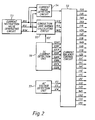
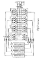
- This invention relates to a power conversion system, and more particularly to a power conversion system wherein a plurality of unit converters are operated connected in parallel.
- Phase angle instruction value is supplied to phase detection circuit 60 and triangular wave generator 61.
- Signals S2 to S5 are the output signals of triangular wave generator 61, and are triangular waves whose period is 60° of the phase angle instruction value.
- Triangular waves S3 to S5 lag in phase by 15° in each case respectively with respect to triangular wave S2, for improving the waveform of the AC output currents of the power conversion system composed of multiple converters 5 to 8.
- Comparator 62 compares amplitude instruction value S1 with triangular waves S2 to S5; the range in which amplitude instruction value S1 is larger than triangular waves S2 to S5 is taken as the output instruction for the AC current.
- Output instruction from comparator 62 and output of phase detection circuit 60 are supplied to logic circuit 63, which generates output instructions S6 to S13 of the AC currents of each of converters 5 to 8 by phase discrimination using the output of phase detection circuit 60.
- S6 is a U-phase output instruction of converter 5.
- S7 is an X-phase output instruction of converter 5.
- S8 is a U-phase output instruction of converter 6.
- S9 is an X-phase output instruction of converter 6.
- S10 is a U-phase output instruction of converter 7.
- S11 is an X-phase output instruction of converter 7.
- S12 is a U-phase output instruction of converter 8.
- S13 is an X-phase output instruction of converter 8.
- the GTOs 9 to 32 of converters 5 to 8 are on/off controlled in accordance with the above output instructions S6 to S13, so that a squarewave waveform current as shown at S14 in Fig. 9 is obtained as the U-phase output current.
- S15 is a UV-phase line voltage of AC load 1. Control is exercised in like manner for the V-phase and W-phase, delaying the phase by 120° in each case with respect to the U-phase.
- S16 to S19 are DC voltages of the converters 5 to 8 when operation is conducted as above.
- S16 is a DC voltage of converter 5
- S17 is a DC voltage of converter 6
- S18 is a DC voltage of converter 7
- S19 is a DC voltage of converter 8.
- one object of this invention is to provide a power conversion system composed of a plurality of unit converters connected in parallel in which DC currents of the unit converters may be better balanced.
- Another object of this invention is to provide a power conversion system composed of a plurality of unit converters connected in parallel which may simplify the DC power source circuitry.
- a power conversion system including a DC power source, a plurality of unit converters, a plurality of DC reactors and a control circuit.
- Each of the unit converters is composed of a bridge connected switching devices for converting a DC power to an AC power.
- Each of the DC reactors is provided between the DC power source and one of the unit converters, respectively.
- Each of the unit converters has DC terminals connected to the DC power source through one of the DC reactors, respectively, and has AC terminals of each phase. The AC terminals of each phase of the unit converters are connected in common and are adapted for connecting to an AC load.
- the control circuit includes a current instruction value generating circuit for generating current instruction values of each phase for AC output currents of each phase of the power conversion system, an AC voltage detection unit for detecting AC output voltages of each phase of the power conversion system, and a DC current detection unit for detecting a plurality of DC currents, each flowing between the DC power source and one of the unit converters, respectively.
- the control circuit also includes a conduction arm number calculating circuit for determining conduction arm numbers of the unit converters of each phase, each being determined based on a ratio of the current instruction value of respective phase and a mean value of the DC currents.
- the control circuit further includes a current balance control circuit connected to receive the conduction arm numbers from the conduction arm number calculating circuit, the AC output voltages from the AC voltage detection unit, and the DC currents from the DC current detection unit, for generating a plurality of conduction instructions for the switching devices at a time of change of one of the conduction arm numbers based on a first order of magnitude of the AC voltages, a second order of magnitude of the DC currents and the conduction arm numbers of each phase at that point.
- the conduction instructions are applied to the unit converters for switching ON or OFF the switching devices, thereby to reduce difference between the DC currents of the unit converters or to exercise balance control therebetween.
- the current balance control circuit outputs conduction instructions based on the orders of magnitudes in which these are arranged and the conduction arm numbers of each phase at that time.
- the switching devices in each unit converter are on/off controlled in accordance with the conduction instructions, so that the DC currents of the plurality of unit converters as a whole is balanced.
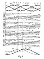
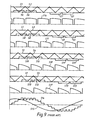
- Fig. 3 and Fig. 4 show the operational waveforms of different portions of unit converters 5 to 8 at the same timing during the period from a time point t1 to a time point t2.
- converter 5 will be called converter A
- converter 6 will be called converter B
- converter 7 will be called converter C
- converter 8 will be called converter D, as shown in Fig. 1.
- the symbols of the positive arms of each of converters 5 to 8 will be specified as U, V, and W, while the symbols of the negative arms thereof will be specified as X, Y and Z, as shown in Fig. 1.
- RIU, RIV and RIW are outputs of current instruction value generating circuit 53, and are applied to current phase detection circuit 54 and conduction arm number calculating circuit 55.
- RIU is a U-phase current instruction value
- RIV is a V-phase current instruction value
- RIW is a W-phase current instruction value.
- IUX, IVX, and IWX are outputs of conduction arm number calculating circuit 55, and show the numbers of conduction arms of U, V and W phases, respectively.
- IUX, IVX and IWX are instruction values of the conduction arm numbers corresponding to current instruction values RIU, RIV and RIW, respectively.
- Conduction number instruction values IUX, IVX and IWX are applied to current balance control circuit 58.
- IDAP to IDDN are the detection values of the DC current of unit converters 5 to 8, which are detected by current detectors 45 to 52, respectively.
- IDAP is a positive side DC current of converter A
- IDBP is a positive side DC current of converter B
- IDCP is a positive side DC current of converter C
- IDDP is a positive side DC current of converter D.
- IDAN is a negative side DC current of converter A
- IDBN is a negative side DC current of converter B
- IDCN is a negative side DC current of converter C
- IDDN is a negative side DC current of converter D.
- the detection values IDAP to IDDN are applied to current balance control circuit 58.
- this invention since this invention has the object of exercising balance control such that the DC currents IDAP to IDDN are equal, and is characterized in that selection control is performed of the conduction arms of converters A to D in accordance with the magnitudes of DC currents IDAP to IDDN.
- the waveforms of DC currents IDAP, IDBP, IDCP and IDDP of Fig. 4 are shown with their deviations with respect to the mean value magnified by a factor of 20.
- VU, VV and VW are phase voltages of AC load 1 and these voltages are detected by voltage detectors (not shown).
- VU is a U-phase voltage
- VV is a V-phase voltage
- VW is a W-phase voltage.
- VUV is a line voltage between the U-phase and V-phase of AC load 1.
- IUAto IZD are the outputs of current balance control circuit 58.
- IUA, IVA, IWA, IXA, IYA, and IZA are conduction instructions of the U, V, W, X, Y and Z phase arms of converter A, respectively.
- IUB, IVB, IWB, IXB, IYB and IZB are conduction instructions of the U, V, W, X, Y and Z phase arms of converter B, respectively.
- IUC, IVC, IWC, IXC, IYC and IZC are conduction instructions of the U, V, W, X, Y and Z phase arms of converter C, respectively.
- IUD, IVD, IWD, IXD, IYD and IZD are conduction instructions of the U, V, W, X, Y and Z phase arms of converter D.
- VDAP is a positive DC voltage of converter A
- VDBP is a positive DC voltage of converter B
- VDCP is a positive DC voltage of converter C
- VDDP is a positive DC voltage of converter D, and these voltages are detected by voltage detectors (not shown).
- the negative DC voltages VDAN to VDDN of converters A to D detected by voltage detectors (not shown) are not shown in Figs. 3 and 4.
- VLAP is a voltage applied to DC reactor 33
- VLBP is a voltage applied to DC reactor 34
- VLCP is a voltage applied to DC reactor 35
- VLDP is a voltage applied to DC reactor 36, and these voltages are detected by voltage detectors (not shown).
- Voltages VLAN to VLDN applied to DC reactors 37 to40 detected by voltage detectors (not shown) are not shown in Figs. 3 and 4.
- VDP is a mean value of positive DC voltages VDAP to VDDP of converters A to D. The following relationship exists:
- Conduction arm number calculating circuit 55 generates conduction number instruction value IUX of the U-phase by carrying out the following calculation.
- IDC is a mean value of positive side DC currents IDAP to IDDP or negative side DC currents IDAN to IDDN.
- Mean value IDC is applied to conduction arm number calculating circuit 55 from DC current detection unit 56.
- Conduction number instruction value IVX of the V-phase, and conduction number instruction value IWX of the W-phase are found based on current instruction values RIV, RIW and mean value IDC, respectively, in the same way, as in the U-phase described above.
- Current phase detection circuit 54 detects the phase of the current every 60° at which the absolute value of RIU, the absolute value or RIV or the absolute value or RIW is a maximum. For example, during the period from a time point t3 to a time point t6 in Fig. 3, the absolute value of V-phase current instruction value RIV is a maximum and V-phase current instruction value RIV is negative.
- Current balance control circuit 58 generates a conduction instruction as follows in accordance with the output signal of current phase detection circuit 54, including a maximum phase at which the absolute value of the current instruction value is a maximum and a polarity of the current instruction value of the maximum phase.
- Signals IYA, IYB, IYC and IYD are made “1" with the timing of the change of signal IWX or signal IUX, causing arm Y of converter A, arm Y of converter B, arm Y of converter C and arm Y of converter D to conduct. That is, at time point t4, when IUX changes from 0 to 1, IYC is changed from "0" to "1". IYA, IYB and IYD are already "1" at time point t4, and so remain unchanged.
- Signals IUA, IUB, IUC and IUD are made "1" with the timing of change of signal IVX or signal IWX, causing arm U of converter A, arm U of converter B, arm U of converter C and arm U of converter D to conduct.
- Signals IZA, IZB, IZC and IZD are made "1" with the timing at which signal IUX or signal IVX changes, causing arm Z of converter A, arm Z of converter B, arm Z of converter C, and arm Z of converter D to conduct.
- Signals IVA, IVB, IVC and IVD are made "1" with the timing at which signal IWX or signal IUX changes, causing arm V of converter A, arm V of converter B, arm V of converter C, and arm V of converter D to conduct.
- Signals IXA, IXB, IXC and IXD are made "1" with the timing at which signal IVX or signal IWX changes, causing arm X of converter A, arm X of converter B, arm X of converter C, and arm X of converter D to conduct.
- Signals IWA, IWB, IWC and IWD are made "1" with the timing at which signal IUX or signal IVX changes, causing arm W of converter A, arm W of converter B, arm W of converter C, and arm W of converter D to conduct.
- control is exercised as follows.
- IUX changes from 0 to 1.
- IWX is 3.
- the conduction number of U-phases of converters A to D is 1
- the conduction number of W-phases of converters A to D is 3.
- the conduction number of the V-phase the multiple number of converters A to D is 4 and the sum of the conduction numbers of the U-phase and W-phase is 4, so the conduction number of the V-phase is 0.
- Balance control of the DC currents can then be performed by making connection from the converter of largest DC current to the phase of largest AC voltage sequentially in accordance with the instruction values of the conduction numbers for each phase. So:
- current balance control circuit 58 generates conduction instructions IUA to IZD to unit converters A to D as follows:
- IWD is made “1"
- IUD, IVD are made “0”.
- IWX changes from 3 to 2.
- IUX is 1. Consequently, the conduction number of the U-phases of converters A to D is 1, and the conduction number of the W-phases of converters A to D is 2.
- the multiple number of converters Ato D is 4, and the total of the conduction number of the U-phase and conduction number of the W-phase is 3, so the conduction number of the V-phases is 1.
- current balance control circuit 58 generates conduction instructions IUA to IZD as follows:
- IVD is made “1" and IWD, IUD are made “0".
- Arms U, V, W, X, Y and Z of converter B are controlled by signals IUB, IVB, IWB, IXB, IYB and IZB, respectively.
- Arms U, V, W, X, Yand Z of converter C are controlled by signals IUC, IVC, IWC, IXC, IYC and IZC, respectively.
- Arms U, V, W, X, Y and Z of converter D are controlled by signals IUD, IVD, IWD, IXD, IYD and IZD, respectively.
- a current IU shown in Fig. 3 is the total value of the U-phase currents of converter A, converter B, converter C and converter D obtained by control as above. It is found that as current IU, a current whose waveforms is like a sine waveform is obtained that tracks instruction value RIU of the U-phase current. Though not shown in Fig. 3, the same applies to V-phase current IV and W-phase current IW. To facilitate understanding of the operation of this invention, the deviations of the positive side DC currents IDAP to IDDP with respect to the mean value are shown multiplied by a factor of 20. As can be found in Fig. 4, good balance control is achieved. Balance control can be likewise exercised in respect of the negative side DC currents IDAN to IDDN by current balance control circuit 58, in which negative side DC currents IDAN to IDDP are used for balance control instead of positive side DC currents IDAP to IDDP as described above.
- balance control of the DC current is performed at the timing at which one of instruction values IUX, IVX, IWX of the conduction numbers of each phase changes. But, if balance control is exercised also when the deviation of the DC current exceeds a fixed limiting value, in addition at the timing at which one of instruction values IUX, IVX or IWX changes, the deviation of the DC current can be further reduced.
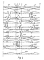
- a power conversion system according to another embodiment of this invention is described with reference to Fig. 5 and Fig. 6, in which balance control is also carried out when the deviation of the DC current exceeds a fixed limit value.
- symbols which are the same as corresponding symbols in Fig. 3 and Fig. 4 indicate the same items, so repeated description is omitted.
- Fig. 5 and Fig. 6 show the operational waveforms of different parts of unit converters Ato D at the same timing from a time point t11 to a time point t12. The operation of this embodiment of this invention will now be described with reference to Fig. 1, Fig. 2, Fig. 5 and Fig. 6.
- V-phase current instruction value RIV in the period from a time point t13 to a time point t16, the absolute value of V-phase current instruction value RIV is a maximum and V-phase current instruction value RIV is negative just as in the period from time point t3 to time point t6 in Fig. 3 and Fig. 4. Consequently, by making signals IYA, IYB, IYC, IYD "1" with the timing at which signal IWX or signal IUX changes, arm Y of converter A, arm Y of converger B, arm Y of converter C and arm Y of converter D conduct. (3) DC balance control when the instruction value of the conduction number changes
- IUX changes from 2 to 3.
- IWX is 1. Consequently, the conduction number of U-phases of converters A to D is 3, while the conduction number of W-phases of converters A to D is 1.
- the multiple number of converters A to D is 4 and the total of the conduction number of the U-phase and conduction number of the W-phase is 4, so the conduction number of the V-phase is 0.
- Balance control of the DC currents can be achieved by making connection from the converter of largest DC current to the phase of largest AC voltage, in order, in accordance with the instruction values of the conduction numbers for each phase. So:
- current balance control circuit 58 generates conduction instructions IUA to IZD as follows:
- IWC is made “1"
- IUC, IVC are made “0”.
- IDCP > IDBP > IDDP > IDAP
- Balance control of the DC current can be achieved by making connection from the converter of largest DC current to the phase of largest AC voltage, in order, in accordance with the instruction values of the conduction numbers of each phase. So:
- current balance control circuit 58 generates conduction instructions IUA to IZD as follows:
- balance control of positive side DC currents IDAP to IDDP can be achieved with a smaller deviation than in the case of Fig. 4.
- Balance control can be carried out in the same way for negative side DC currents IDAN to IDDN.
- the DC current values of each unit converter, and AC voltages of each phase are arranged in order of magnitude, respectively, and on/off control of the switching devices in each unit converter is exercised in accordance with these arrangement orders and the number of conduction arms in each phase at that point. Thanks to the adoption of a construction as above, current balance can be obtained even using only a single DC power source device. This enables the power source circuitry to be simplifed.
Landscapes
- Engineering & Computer Science (AREA)
- Power Engineering (AREA)
- Inverter Devices (AREA)
- Rectifiers (AREA)
Applications Claiming Priority (3)
| Application Number | Priority Date | Filing Date | Title |
|---|---|---|---|
| JP03029094A JP3297184B2 (ja) | 1994-02-28 | 1994-02-28 | 電力変換装置 |
| JP30290/94 | 1994-02-28 | ||
| JP3029094 | 1994-02-28 |
Publications (3)
| Publication Number | Publication Date |
|---|---|
| EP0669705A2 true EP0669705A2 (de) | 1995-08-30 |
| EP0669705A3 EP0669705A3 (de) | 1996-08-28 |
| EP0669705B1 EP0669705B1 (de) | 1999-12-22 |
Family
ID=12299603
Family Applications (1)
| Application Number | Title | Priority Date | Filing Date |
|---|---|---|---|
| EP95301247A Expired - Lifetime EP0669705B1 (de) | 1994-02-28 | 1995-02-27 | Leistungswandlungssystem |
Country Status (4)
| Country | Link |
|---|---|
| US (1) | US5576944A (de) |
| EP (1) | EP0669705B1 (de) |
| JP (1) | JP3297184B2 (de) |
| DE (1) | DE69514015T2 (de) |
Families Citing this family (6)
| Publication number | Priority date | Publication date | Assignee | Title |
|---|---|---|---|---|
| US5798916A (en) * | 1997-03-20 | 1998-08-25 | Electric Power Research Institute, Inc. | High power inverter pole employing series connected devices configured for reduced stray loop inductance |
| US5889668A (en) * | 1997-09-05 | 1999-03-30 | Electric Power Research Institute, Inc. | Three-phase DC-to-AC power inverter with three-level poles |
| JP3290947B2 (ja) * | 1998-03-12 | 2002-06-10 | 株式会社東芝 | 電力変換器 |
| KR101147524B1 (ko) * | 2011-09-27 | 2012-05-21 | 버추얼모션(주) | 사고전류 차단용 전력소자의 전류분배장치 |
| AT512886B1 (de) * | 2012-04-26 | 2014-03-15 | Siemens Ag | Verfahren und Vorrichtung zur Einstellung der Verzögerungszeit eines Halbleiterventils |
| US9088203B2 (en) * | 2012-07-26 | 2015-07-21 | General Electric Company | Current balance for a multi-phase electric power converter and method for operating the same |
Family Cites Families (3)
| Publication number | Priority date | Publication date | Assignee | Title |
|---|---|---|---|---|
| JPS605151B2 (ja) * | 1978-04-05 | 1985-02-08 | 株式会社日立製作所 | 多重化電流形インバ−タの制御方法 |
| JPS5828837B2 (ja) * | 1978-12-27 | 1983-06-18 | 株式会社東芝 | 交流電動機の制御装置 |
| US5070440A (en) * | 1990-08-14 | 1991-12-03 | General Electric Company | Power conversion scheme employing paralleled units |
-
1994
- 1994-02-28 JP JP03029094A patent/JP3297184B2/ja not_active Expired - Fee Related
-
1995
- 1995-02-02 US US08/382,585 patent/US5576944A/en not_active Expired - Fee Related
- 1995-02-27 DE DE69514015T patent/DE69514015T2/de not_active Expired - Fee Related
- 1995-02-27 EP EP95301247A patent/EP0669705B1/de not_active Expired - Lifetime
Also Published As
| Publication number | Publication date |
|---|---|
| JPH07241082A (ja) | 1995-09-12 |
| DE69514015D1 (de) | 2000-01-27 |
| DE69514015T2 (de) | 2000-07-06 |
| US5576944A (en) | 1996-11-19 |
| EP0669705B1 (de) | 1999-12-22 |
| JP3297184B2 (ja) | 2002-07-02 |
| EP0669705A3 (de) | 1996-08-28 |
Similar Documents
| Publication | Publication Date | Title |
|---|---|---|
| US5016158A (en) | Parallel multi-inverter system and motor drive system using the same | |
| US11601064B2 (en) | Power conversion device having a frequency of a first control signal higher than a frequency of a second control signal | |
| US5566061A (en) | Power conversion system and control device therefor | |
| EP4586490A1 (de) | Mehrstufiger wechselrichter | |
| CA2087832C (en) | Method and apparatus for controlling an inverter | |
| EP3890134B1 (de) | Leistungssteuerungssystem | |
| EP4586489A1 (de) | Mehrstufiger wechselrichter | |
| JP2013162536A (ja) | 電力変換装置 | |
| WO2021186524A1 (ja) | 電力変換装置 | |
| US5436823A (en) | Parallel operation controller for power converters | |
| US5576944A (en) | Plural parallel bridge inverter power conversion system with balanced DC input currents | |
| JP3903429B2 (ja) | 電力変換装置 | |
| CN106160540A (zh) | 电力变换装置 | |
| JP7040077B2 (ja) | 電力変換装置 | |
| JP3509094B2 (ja) | 三相/単相pwmサイクロコンバータの制御装置 | |
| JP7249238B2 (ja) | 直列多重電力変換装置 | |
| JP3431472B2 (ja) | 電力変換装置 | |
| JP5924353B2 (ja) | 直列多重マトリクスコンバータおよび電動機駆動装置 | |
| JP2018182841A (ja) | マルチレベル電力変換回路 | |
| JPH05268773A (ja) | Pwm制御を用いたインバータの制御方法及び装置 | |
| Pulikanti et al. | SHE-PWM switching strategies for active neutral point clamped multilevel converters | |
| JP3192858B2 (ja) | 電力変換装置の制御装置 | |
| JP2004242390A (ja) | 交流−交流電力変換器の制御装置 | |
| JP7743369B2 (ja) | 電力変換装置 | |
| JP5517911B2 (ja) | 電力変換システム |
Legal Events
| Date | Code | Title | Description |
|---|---|---|---|
| PUAI | Public reference made under article 153(3) epc to a published international application that has entered the european phase |
Free format text: ORIGINAL CODE: 0009012 |
|
| 17P | Request for examination filed |
Effective date: 19950323 |
|
| AK | Designated contracting states |
Kind code of ref document: A2 Designated state(s): DE FR GB SE |
|
| PUAL | Search report despatched |
Free format text: ORIGINAL CODE: 0009013 |
|
| AK | Designated contracting states |
Kind code of ref document: A3 Designated state(s): DE FR GB SE |
|
| 17Q | First examination report despatched |
Effective date: 19971029 |
|
| GRAG | Despatch of communication of intention to grant |
Free format text: ORIGINAL CODE: EPIDOS AGRA |
|
| GRAG | Despatch of communication of intention to grant |
Free format text: ORIGINAL CODE: EPIDOS AGRA |
|
| GRAH | Despatch of communication of intention to grant a patent |
Free format text: ORIGINAL CODE: EPIDOS IGRA |
|
| GRAH | Despatch of communication of intention to grant a patent |
Free format text: ORIGINAL CODE: EPIDOS IGRA |
|
| GRAA | (expected) grant |
Free format text: ORIGINAL CODE: 0009210 |
|
| AK | Designated contracting states |
Kind code of ref document: B1 Designated state(s): DE FR GB SE |
|
| REF | Corresponds to: |
Ref document number: 69514015 Country of ref document: DE Date of ref document: 20000127 |
|
| ET | Fr: translation filed | ||
| PLBE | No opposition filed within time limit |
Free format text: ORIGINAL CODE: 0009261 |
|
| STAA | Information on the status of an ep patent application or granted ep patent |
Free format text: STATUS: NO OPPOSITION FILED WITHIN TIME LIMIT |
|
| 26N | No opposition filed | ||
| PGFP | Annual fee paid to national office [announced via postgrant information from national office to epo] |
Ref country code: SE Payment date: 20010206 Year of fee payment: 7 |
|
| PGFP | Annual fee paid to national office [announced via postgrant information from national office to epo] |
Ref country code: FR Payment date: 20010213 Year of fee payment: 7 |
|
| PGFP | Annual fee paid to national office [announced via postgrant information from national office to epo] |
Ref country code: GB Payment date: 20010221 Year of fee payment: 7 Ref country code: DE Payment date: 20010221 Year of fee payment: 7 |
|
| REG | Reference to a national code |
Ref country code: GB Ref legal event code: IF02 |
|
| PG25 | Lapsed in a contracting state [announced via postgrant information from national office to epo] |
Ref country code: GB Free format text: LAPSE BECAUSE OF NON-PAYMENT OF DUE FEES Effective date: 20020227 |
|
| PG25 | Lapsed in a contracting state [announced via postgrant information from national office to epo] |
Ref country code: SE Free format text: LAPSE BECAUSE OF NON-PAYMENT OF DUE FEES Effective date: 20020228 |
|
| PG25 | Lapsed in a contracting state [announced via postgrant information from national office to epo] |
Ref country code: DE Free format text: LAPSE BECAUSE OF NON-PAYMENT OF DUE FEES Effective date: 20020903 |
|
| EUG | Se: european patent has lapsed |
Ref document number: 95301247.3 |
|
| GBPC | Gb: european patent ceased through non-payment of renewal fee |
Effective date: 20020227 |
|
| PG25 | Lapsed in a contracting state [announced via postgrant information from national office to epo] |
Ref country code: FR Free format text: LAPSE BECAUSE OF NON-PAYMENT OF DUE FEES Effective date: 20021031 |
|
| REG | Reference to a national code |
Ref country code: FR Ref legal event code: ST |