EP0657883A2 - Informationswiedergabegerät und -methode - Google Patents
Informationswiedergabegerät und -methode Download PDFInfo
- Publication number
- EP0657883A2 EP0657883A2 EP94309223A EP94309223A EP0657883A2 EP 0657883 A2 EP0657883 A2 EP 0657883A2 EP 94309223 A EP94309223 A EP 94309223A EP 94309223 A EP94309223 A EP 94309223A EP 0657883 A2 EP0657883 A2 EP 0657883A2
- Authority
- EP
- European Patent Office
- Prior art keywords
- signal
- comparing
- output
- reference signal
- binary
- Prior art date
- Legal status (The legal status is an assumption and is not a legal conclusion. Google has not performed a legal analysis and makes no representation as to the accuracy of the status listed.)
- Ceased
Links
- 238000000034 method Methods 0.000 title claims description 12
- 230000001360 synchronised effect Effects 0.000 claims abstract description 52
- 230000004044 response Effects 0.000 claims description 3
- 230000001960 triggered effect Effects 0.000 claims description 2
- 238000010586 diagram Methods 0.000 description 30
- 230000003287 optical effect Effects 0.000 description 20
- 238000001514 detection method Methods 0.000 description 6
- 239000003990 capacitor Substances 0.000 description 5
- 238000012935 Averaging Methods 0.000 description 4
- 238000010276 construction Methods 0.000 description 4
- 238000007599 discharging Methods 0.000 description 4
- 230000015654 memory Effects 0.000 description 4
- 230000000694 effects Effects 0.000 description 3
- 230000005856 abnormality Effects 0.000 description 2
- 238000003708 edge detection Methods 0.000 description 2
- 238000013459 approach Methods 0.000 description 1
- 230000003139 buffering effect Effects 0.000 description 1
- 230000003111 delayed effect Effects 0.000 description 1
- 239000000428 dust Substances 0.000 description 1
- 230000010355 oscillation Effects 0.000 description 1
- 230000002093 peripheral effect Effects 0.000 description 1
- 229920000729 poly(L-lysine) polymer Polymers 0.000 description 1
- 230000003252 repetitive effect Effects 0.000 description 1
Images


Classifications
-
- G—PHYSICS
- G11—INFORMATION STORAGE
- G11B—INFORMATION STORAGE BASED ON RELATIVE MOVEMENT BETWEEN RECORD CARRIER AND TRANSDUCER
- G11B11/00—Recording on or reproducing from the same record carrier wherein for these two operations the methods are covered by different main groups of groups G11B3/00 - G11B7/00 or by different subgroups of group G11B9/00; Record carriers therefor
- G11B11/10—Recording on or reproducing from the same record carrier wherein for these two operations the methods are covered by different main groups of groups G11B3/00 - G11B7/00 or by different subgroups of group G11B9/00; Record carriers therefor using recording by magnetic means or other means for magnetisation or demagnetisation of a record carrier, e.g. light induced spin magnetisation; Demagnetisation by thermal or stress means in the presence or not of an orienting magnetic field
- G11B11/105—Recording on or reproducing from the same record carrier wherein for these two operations the methods are covered by different main groups of groups G11B3/00 - G11B7/00 or by different subgroups of group G11B9/00; Record carriers therefor using recording by magnetic means or other means for magnetisation or demagnetisation of a record carrier, e.g. light induced spin magnetisation; Demagnetisation by thermal or stress means in the presence or not of an orienting magnetic field using a beam of light or a magnetic field for recording by change of magnetisation and a beam of light for reproducing, i.e. magneto-optical, e.g. light-induced thermomagnetic recording, spin magnetisation recording, Kerr or Faraday effect reproducing
- G11B11/10502—Recording on or reproducing from the same record carrier wherein for these two operations the methods are covered by different main groups of groups G11B3/00 - G11B7/00 or by different subgroups of group G11B9/00; Record carriers therefor using recording by magnetic means or other means for magnetisation or demagnetisation of a record carrier, e.g. light induced spin magnetisation; Demagnetisation by thermal or stress means in the presence or not of an orienting magnetic field using a beam of light or a magnetic field for recording by change of magnetisation and a beam of light for reproducing, i.e. magneto-optical, e.g. light-induced thermomagnetic recording, spin magnetisation recording, Kerr or Faraday effect reproducing characterised by the transducing operation to be executed
- G11B11/10515—Reproducing
-
- G—PHYSICS
- G11—INFORMATION STORAGE
- G11B—INFORMATION STORAGE BASED ON RELATIVE MOVEMENT BETWEEN RECORD CARRIER AND TRANSDUCER
- G11B20/00—Signal processing not specific to the method of recording or reproducing; Circuits therefor
- G11B20/10—Digital recording or reproducing
- G11B20/10009—Improvement or modification of read or write signals
-
- G—PHYSICS
- G11—INFORMATION STORAGE
- G11B—INFORMATION STORAGE BASED ON RELATIVE MOVEMENT BETWEEN RECORD CARRIER AND TRANSDUCER
- G11B20/00—Signal processing not specific to the method of recording or reproducing; Circuits therefor
- G11B20/10—Digital recording or reproducing
- G11B20/14—Digital recording or reproducing using self-clocking codes
- G11B20/1403—Digital recording or reproducing using self-clocking codes characterised by the use of two levels
-
- G—PHYSICS
- G11—INFORMATION STORAGE
- G11B—INFORMATION STORAGE BASED ON RELATIVE MOVEMENT BETWEEN RECORD CARRIER AND TRANSDUCER
- G11B20/00—Signal processing not specific to the method of recording or reproducing; Circuits therefor
- G11B20/10—Digital recording or reproducing
- G11B20/12—Formatting, e.g. arrangement of data block or words on the record carriers
- G11B20/1217—Formatting, e.g. arrangement of data block or words on the record carriers on discs
- G11B20/1258—Formatting, e.g. arrangement of data block or words on the record carriers on discs where blocks are arranged within multiple radial zones, e.g. Zone Bit Recording or Constant Density Recording discs, MCAV discs, MCLV discs
Definitions
- the present invention relates to an optical information reproducing apparatus for binarizing a reproduction signal from an optical information recording medium.
- optical recording media such as an optical disc and the like are rapidly being advanced as memories of a high density and a large capacity including a rewritable magnetooptical disc as well as a read only CD and a write once type disc.
- the magnetooptical disc is expected as an external memory of a high density and a large capacity of a computer.
- a mark position recording such that when information is recorded on the disc, "1" of the information is recorded as a pit of a single length has been used.
- a mark edge recording such that by providing information for edges on both sides of a pit, a higher density can be realized even in case of the same pit is becoming a main stream.
- Figs. 1A to 1C are waveform diagrams showing changes in reproduction signal when a writing level of a magnetooptical signal is changed.
- Fig. 1A shows the reproduction signal when it was written at an excessive level.
- Fig. 1B shows the reproduction signal when it was written at a proper level.
- Fig. 1C shows the reproduction signal when it was written at an under level.
- the slice level to be set at the center value of the peak and bottom values is improper, so that the pulse width to be inherently reproduced cannot be reproduced and output.
- Fig. 2 shows a problem which is caused due to the influence by the DC component.
- a reproduction waveform as shown in the diagram appears in dependence on a modulation pattern.
- a block B in case of a block A, if the center value of the peak and bottom values is set to a slice level, a correct pulse width cannot be reproduced.
- reference numeral 51 denotes a peak-hold circuit; 52 a bottom-hold circuit; 53 a center level detection circuit; 54 a comparator; 55 a leading edge detection circuit; 56 a trailing edge detection circuit; 57 and 59 phase locked loop (PLL) circuit; 60 and 61 synchronous circuits; 62 and 63 first-in first-out memory circuits (FiFo circuits); and 64 a data composition circuit.
- PLL phase locked loop
- a center value which is detected by the center level detection circuit 53 from outputs of the peak-hold circuit 51 and bottom-hold circuit 52 is set to a slice level and a binarization is coarsely performed by the comparator 54.
- Different PLLs are applied at the leading and trailing edges of a binary signal and the resultant reproduction data is inputted to the FiFo circuits 62 and 63. Subsequently, by reading out the reproduction data by a clock which is generated on the controller side, a fluctuation in recording power, a fluctuation in amplitude, and an influence by the DC component are reduced.
- the present invention is made in consideration of the above problems and it is a concern of the invention to provide an optical information reproducing apparatus which can reproduce an accurate magnetooptical signal and can perform a binarization of a high response speed and a high precision irrespective of complicated fluctuations in level of a reproduction signal and a duty due to a change in writing level or the like of the magnetooptical signal.
- an information reproducing apparatus having first comparing means for comparing a reproduction signal from an information recording medium and a first reference signal, thereby binarizing, clock signal generating means for generating a clock signal from a signal binarized by the first comparing means, and synchronous means for synchronizing the binary signal by the clock signal
- the information reproducing apparatus comprises: phase comparing means for comparing a phase of the binary signal and a phase of an output of the synchronous means; a charge/discharge circuit which is driven by an output of the phase comparing means; second comparing means for comparing an output of the charge/discharge circuit and a second reference signal; and control means for controlling the first reference signal by an output of the second comparing means synchronously with the binary signal or an output of the synchronous means.
- an information reproducing method having a step of comparing a reproduction signal from an information recording medium and a first reference signal, thereby binarizing the reproduction signal and a step of generating a clock signal from the binary signal and synchronizing the binary signal by the clock signal, wherein the information reproducing method comprises: a first comparing step of comparing a phase of the binary signal and a phase of the synchronized signal; a step of charging or discharging in accordance with a signal outputted in the first comparing step; a second comparing step of comparing a voltage generated by the charge or discharge and a second reference signal; a step of synchronizing a signal outputted in the second comparing step with the binary signal or the synchronized signal; and a step of controlling the first reference signal by a signal outputted in the synchronizing step.
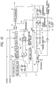
- Fig. 4 is a block diagram showing the first embodiment of an optical information reproducing apparatus of the invention.
- a DATAIN signal (a) is a reproduction signal of a mark edge format which is obtained by a method whereby a reproduction signal reproduced by an optical head (not shown) is amplified by a preamplifier (not shown) and is subsequently waveform equalized.
- Reference numeral 1 denotes a peak-hold circuit for detecting a positive peak of the reproduction signal (a) and holding it by a predetermined time constant and detecting a positive envelope; 2 a bottom-hold circuit for detecting a negative peak of the signal (a) and holding it by a predetermined time constant and detecting a negative envelope; 3 a center level detection circuit which is connected to an output of the peak-hold circuit 1 and an output of the bottom-hold circuit 2 and detects a center signal of the above two envelope signals; and 4 a track/hold circuit.
- the track/hold circuit 4 operates as a buffer and charges or discharges a capacitor of a first reference voltage shown as a reference 1 and directly outputs the center level signal as it is.
- the SLHOLD signal is at the low level
- an output of the track/hold circuit is set into a high impedance state and the value so far is held in the capacitor of the first reference voltage.
- Reference numeral 5 denotes a first voltage comparator for comparing the reproduction signal and the first reference voltage and converting the reproduction signal to a digital binary signal; 6 a data separator for extracting a clock synchronized with the reproduction signal binarized by the first voltage comparator 5 from such a binary reproduction signal and for supplying the synchronous data converted into the mark position format and the sync clock to a disc controller (not shown) at the next stage; 7 a synchronous circuit for synchronizing the reproduction signal binarized by the voltage comparator 5 with the sync clock from the data separator 6; 8 a phase comparison circuit for comparing a phase of the reproduction signal binarized by the voltage comparator 5 and a phase of a sync binary signal synchronized with the sync clock in the synchronous circuit 7; 9 a charge/discharge circuit (charge pump circuit here, for example) which is charged or discharged on the basis of the comparison result of the phase comparison circuit 8; 10 a second voltage comparator for comparing an output of the charge pump circuit 9 and a second reference voltage;
- the drive means 13 comprises a voltage source, a capacitor C, and a resistor R and switches SW1 and SW2 connected between them.
- a cut-off frequency that is decided by the values of the resistor R and capacitor C is set to a value which is lower than the highest frequency of the input signal and is higher than 1/20 of the lowest frequency of the input signal.
- Fig. 5A is a diagram showing a magnetooptical signal.
- Fig. 5B is a diagram showing the relation between the magnetooptical signal and the slice level. The slice level has been set to the center value between the peak value and bottom value of the average amplitude of the magnetooptical signal in a manner similar to the conventional apparatus, so that the slice level is not the optimum slice level.
- Fig. 5C is a diagram showing the binary signal when the magnetooptical signal is binarized by the slice level in Fig. 5B. Since the slice level is improper, an abnormality occurs in the pulse width like waveforms at the center and right positions shown in the diagram.
- Fig. 5D shows synchronous clocks extracted by the data separator 6.
- Fig. 5E shows an output of the synchronous circuit 7 as a synchronous output signal which is obtained by synchronizing the binary output of Fig. 5C by the synchronous clock. In this case, it will be understood that the pulse width is constant due to the synchronization.
- the slice level is proper. According to the invention, therefore, the slice level is controlled at a high speed so as to equalize the binary output and the synchronous output, thereby always maintaining the slice level to the optimum value and accurately reproducing the reproduction signal.
- a header portion in which information such as a position of a sector on the disc and the like has previously been recorded in recess and projection forms and a data portion in which information is recorded in a magnetooptical disc or the like are reproduced in a form as shown in (a) in Fig. 6.
- (b) in Fig. 6 shows a typical example of a format of the reproduction signal.
- a sector mark (SM) indicative of the head position of the sector is recorded at the head of the header portion.
- a VFO pattern to pull in the PLL is subsequently recorded.
- the VFO pattern is formed by repeating a predetermined pattern (in case of the mark edge recording, a duty ratio is ideally set to 50%) and has a length of about 20 bytes.
- address information an address mark signal indicative of the start position thereof, and the like are recorded.
- a plurality of combinations of such VFO and ID are recorded.
- a VFO to pull in the PLL, a SYNC pattern to detect the head position of the data, and the like are recorded.
- the SLHOLD signal to control the track/hold circuit 4 is set to the high level in the header and the head portion of the VFO pattern of the data portion.
- the track/hold circuit is in a buffer state as mentioned above. Therefore, the center level of the peak-to-peak signal of the reproduction signal formed by the peak-hold circuit and bottom-hold circuit is supplied as a slice level to a first reference voltage.
- the slice level is not perfectly accurate, it is set to a level at which the coarse operation can be performed, so that the operation to pull in the PLL and the like can be executed.
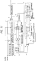
- Fig. 7 shows a signal waveform in each section of the apparatus of Fig. 4.
- (b) to (l) in Fig. 7 show waveforms of signals (b) to (l) shown in Fig. 4.
- the reproduction binary signal and the synchronous binary signal are the signals whose phases are slightly deviated.
- a difference between both of the duty cycles is expressed as a change in widths of charge and discharge pulses to the charge pump circuit 9 as shown in (d) and (e).
- the pulse widths of the charge pulse and discharge pulse are equal and the output level of the charge pump circuit 9 is set to an almost constant value.
- the duty ratio of the reproduction binary signal is smaller than that of the synchronous binary signal [the high level portion of (b) in Fig. 7 is narrow)
- the pulse width on the charging side is narrower than the pulse width on the discharging side.
- the pulse width on the discharging side is narrower than the pulse width on the charging side.
- the output voltage of the charge pump circuit 9 is not a perfectly smooth signal but is a combination of signals like trapezoids each having a predetermined inclination in the portion to discharge. This is because a time constant of the charge pump is set to a small value in order to detect the difference between the duties of two signals at a high speed. A fairly large change during the charging or discharging operation appears.
- a second reference voltage has been preset to a voltage of the bottom side of the trapezoidal portion of the output voltage of the charge pump in the case where the duty cycle of the reproduction binary signal is equal to the duty cycle of the synchronous binary signal.
- An output of the second voltage comparator 10 is as shown in (h) in Fig. 7. This output signal is constructed in a form such that the output of the second voltage comparator 10 is inputted to the input of the D-type flip-flop and the reproduction binary signal is inputted to the clock and they are synchronized.
- Outputs of the synchronous circuit 11 are as shown in (i) and (j) in Fig. 7 and are supplied to the AND gates, respectively.
- the AND gates perform logic operations between the input signals (i) and (j) and an output (k) of the one-shot circuit 12 synchronized with the reproduction binary signal, thereby controlling the switches SW1 and SW2 of the reference voltage drive means 13.
- the first reference voltage is charged or discharged synchronously with the binary reproduction signal in accordance with the difference between the duties of the reproduction binary signal and the synchronous binary signal, thereby controlling the slice level.
- S R denotes a reproduction signal having a DC-like fluctuation or duty fluctuation
- L PH a peak-hold level
- L BH a bottom-hold level
- L S a slice level
- L C a center level between the peak and bottom levels.
- Fig. 9 shows a block diagram of the second embodiment of the invention.
- the same component elements as those shown in Fig. 4 are designated by the same reference numerals and their detailed descriptions are omitted.
- the output of the voltage comparator 10 is converted to the differential output and is inputted to the front gate of the reference voltage drive means 13.
- the other circuit constructions are substantially similar to those in the apparatus of Fig. 4.
- whether the first reference voltage shown at the reference 1 is charged or discharged is determined in accordance with whether the output of the voltage comparator 10 is at the high level or the low level.
- the first reference voltage is charged or discharged synchronously with the output (k) of the one-shot circuit 12.
- Fig. 10 shows a block diagram of the third embodiment of the invention.
- the same component elements as those shown in Fig. 4 are designated by the same reference numerals and their detailed descriptions are omitted.
- a control by an auto control enable signal is added to the apparatus of Fig. 4.
- the auto control enable signal is set to the low level
- the non-inverting input of the voltage comparator 10 is fixed to the second reference voltage by a switch SW4.
- the control by the loop is started, the output of the charge pump circuit 9 starts from the second reference voltage. In this state, a switch SW3 is open and the control loop by the charge pump circuit 9 is inoperative.
- the switch SW4 When the auto control enable signal is set to the high level, the switch SW4 is first opened and the charge or discharge of the charge pump circuit 9 is started and the auto control system is set into an enable state. After that, when the reproduction binary signal is inputted, the switch SW3 is turned on by a D-type flip-flop 15, the charge or discharge to the first reference voltage is started, and the loop of the auto control system is made operative.
- Fig. 11 shows a block diagram of the fourth embodiment of the invention.
- the same component elements as those shown in Fig. 4 are designated by the same reference numerals and their detailed descriptions are omitted.
- the second reference voltage of the apparatus of Fig. 4 is supplied by a D/A converter 17 which is controlled by the CPU.
- a recording method namely, so called a zone bit recording (Z. B.
- Fig. 12 shows a block diagram of the fifth embodiment of the invention.
- the same component elements as those shown in Fig. 4 are designated by the same reference numerals and their detailed descriptions are omitted.
- the one-shot circuit 12 in the apparatus of Fig. 4 is omitted. Even in such a construction, effects similar to those of the apparatus of Fig. 4 are derived.
- Fig. 13 shows a block diagram of the sixth embodiment of the invention.
- the same component elements as those shown in Fig. 4 are designated by the same reference numerals and their detailed descriptions are omitted.
- the synchronous circuit 11 in the apparatus of Fig. 4 is omitted.
- a sample-hold circuit 19 is provided for the output of the charge pump circuit 9 and the output is sampled and held by a one-shot signal of the reproduction binary signal (b), thereby obtaining effects similar to those of the apparatus in Fig. 4.
- Fig. 14 shows a block diagram of the seventh embodiment of the invention.
- the same component elements as those shown in Fig. 4 are designated by the same reference numerals and their detailed descriptions are omitted.
- a circuit to automatically adjust the second reference voltage shown in Fig. 4 is added.
- the switch SW 24 is switched to the lower side (opposite to the side shown in the diagram).
- the reference voltage of the voltage comparator 5 is supplied from a voltage source 23 which is controlled by a driving amplifier 22.
- the average value of an output of a charge/discharge circuit 20 which is charged or discharged in accordance with whether the output of the voltage comparator 5 is at the low level or the high level is inputted to the driving amplifier 22.
- a feedback loop is constructed and the apparatus is feedback controlled so that the duty of the output of the voltage comparator 5 is set to 50%.
- the voltage of the voltage source 23 at this time is compared with the first reference voltage and the data is set into the D/A converter 17 by a controller 25 so that the first reference voltage is equal to the voltage of the voltage source 23.
- the reference voltage of the second voltage comparator is adjusted.
- the delay time of the synchronous means exceeds such a minimum inverting time, as shown in the eighth embodiment of Fig. 15, before the phase of the binary signal (b) is compared with the phase of the output of the synchronous means, the binary signal (b) is delayed by delay means 35 (for example, delay line), thereby setting the time difference between those signals to a value less than the minimum inverting time.
- delay means 35 for example, delay line
- any one of the clock signal which is generated from the data separator 6 and the synchronized binary signal may be used as a clock (CK) input of the synchronous circuit 7.
- CK clock
- the 1-7 RLL in case of using the clock signal, an edge shift of the binary signal in only a range of up to 1T is permitted because of a limitation of the operation of the present circuit.
- the synchronized binary signal in case of using the synchronized binary signal is used, an edge shift in a range of up to 2T is permitted, so that it is desirable.
- the optical information reproducing apparatus of the invention when the duty ratios or pulse widths of the binary signal binarized by the first reference voltage (reference voltage of the voltage comparator for binarization: slice level) is compared with that of the synchronous binary signal synchronized by the clock signal formed by the binary signal, the charge pump circuit of a small time constant is used. The output of the charge pump circuit is compared with the second reference voltage. The result of the comparison is fed back to the first reference voltage synchronously with the binary signal, thereby setting the slice level. Therefore, the binarization of a high response speed and a high precision can be performed irrespective of the complicated fluctuations in level of the reproduction signal and in duty due to a change in writing level of the magnetooptical signal or the like. The accurate magnetooptical signal can be reproduced.
- the first reference voltage reference voltage of the voltage comparator for binarization: slice level
Landscapes
- Engineering & Computer Science (AREA)
- Signal Processing (AREA)
- Signal Processing For Digital Recording And Reproducing (AREA)
- Optical Recording Or Reproduction (AREA)
Applications Claiming Priority (2)
| Application Number | Priority Date | Filing Date | Title |
|---|---|---|---|
| JP31059993A JP3184688B2 (ja) | 1993-12-10 | 1993-12-10 | 光学的情報再生装置 |
| JP310599/93 | 1993-12-10 |
Publications (2)
| Publication Number | Publication Date |
|---|---|
| EP0657883A2 true EP0657883A2 (de) | 1995-06-14 |
| EP0657883A3 EP0657883A3 (de) | 1996-01-10 |
Family
ID=18007199
Family Applications (1)
| Application Number | Title | Priority Date | Filing Date |
|---|---|---|---|
| EP94309223A Ceased EP0657883A3 (de) | 1993-12-10 | 1994-12-09 | Informationswiedergabegerät und -methode. |
Country Status (3)
| Country | Link |
|---|---|
| US (1) | US5592456A (de) |
| EP (1) | EP0657883A3 (de) |
| JP (1) | JP3184688B2 (de) |
Cited By (1)
| Publication number | Priority date | Publication date | Assignee | Title |
|---|---|---|---|---|
| EP1087393A3 (de) * | 1999-09-24 | 2004-03-10 | Sanyo Electric Co., Ltd. | Signalverarbeitungsschaltung und integrierte Halbleiterschaltung |
Families Citing this family (14)
| Publication number | Priority date | Publication date | Assignee | Title |
|---|---|---|---|---|
| US5999506A (en) * | 1996-08-22 | 1999-12-07 | Matsushita Electric Industrial Co., Ltd. | Data recording/reproducing device and recording medium |
| US5966356A (en) * | 1996-11-11 | 1999-10-12 | Konica Corporation | Optimum slice level signal reading apparatus for optical disk |
| DE19715274A1 (de) * | 1997-04-12 | 1998-10-15 | Thomson Brandt Gmbh | Gerät zum Lesen und/oder Beschreiben optischer Aufzeichnungsträger |
| JPH11120564A (ja) * | 1997-10-08 | 1999-04-30 | Toshiba Corp | 光ディスク装置及び光ディスク再生方法 |
| US6091687A (en) * | 1997-12-19 | 2000-07-18 | Philips Electronics N.A. Corporation | Method and apparatus for maximum likelihood detection |
| US6631103B1 (en) * | 1998-04-09 | 2003-10-07 | Texas Instruments Incorporated | Jitter feedback slicer |
| KR100333332B1 (ko) * | 1998-12-17 | 2002-06-20 | 윤종용 | 미러신호 검출을 위한 회로 및 방법과 그를위한 광디스크 장치? |
| JP2001202634A (ja) * | 1999-12-23 | 2001-07-27 | Lg Electronics Inc | 光記録再生器のトラッキング制御方法及び装置 |
| KR100613788B1 (ko) * | 2001-03-30 | 2006-08-22 | 캐논 가부시끼가이샤 | 파일 관리 방법 |
| KR100475091B1 (ko) * | 2002-08-30 | 2005-03-10 | 삼성전자주식회사 | 광디스크 시스템에서의 데이터 슬라이서 및 그 방법 |
| KR100787940B1 (ko) * | 2006-07-07 | 2007-12-24 | 삼성전자주식회사 | 고전압 발생회로 및 그것을 구비한 플래시 메모리 장치 |
| US7541955B2 (en) * | 2006-09-26 | 2009-06-02 | Teac Corporation | A/D conversion circuit and optical disk drive |
| CN102667731A (zh) | 2009-12-25 | 2012-09-12 | 富士通株式会社 | 信号复原电路、等待时间调整电路、存储器控制器、处理器、计算机、信号复原方法以及等待时间调整方法 |
| US10523218B2 (en) | 2017-04-18 | 2019-12-31 | Taiwan Semiconductor Manufacturing Co., Ltd. | Track-and-hold charge pump and PLL |
Citations (1)
| Publication number | Priority date | Publication date | Assignee | Title |
|---|---|---|---|---|
| EP0482823A2 (de) * | 1990-10-22 | 1992-04-29 | Nec Corporation | Frequenzsynthesierer mit PLL, der einen Frequenzwechsel des Ausgangs mit hoher Geschwindigkeit ermöglicht |
Family Cites Families (8)
| Publication number | Priority date | Publication date | Assignee | Title |
|---|---|---|---|---|
| EP0232181B1 (de) * | 1986-02-07 | 1992-09-16 | Matsushita Electric Industrial Co., Ltd. | Gerät zur Wiedergabe von Digitalinformationen |
| JPS62267975A (ja) * | 1986-05-16 | 1987-11-20 | Matsushita Electric Ind Co Ltd | デイジタル信号再生回路 |
| US5204848A (en) * | 1991-06-17 | 1993-04-20 | International Business Machines Corporation | Adjusting amplitude detection threshold by feeding back timing-data phase errors |
| US5388087A (en) * | 1991-07-11 | 1995-02-07 | Hitachi, Ltd. | Recording and reproducing apparatus including changing a reproduction characteristic when an error has occurred in reproduced data |
| JPH0540978A (ja) * | 1991-08-05 | 1993-02-19 | Canon Inc | 光学的情報記録再生装置 |
| JP2807362B2 (ja) * | 1991-09-30 | 1998-10-08 | 株式会社東芝 | 情報再生装置 |
| US5396479A (en) * | 1994-05-06 | 1995-03-07 | Maxoptix Corporation | Apparatus and method for setting a threshold level to maintain duty cycle in a pulse width modulated optical recording system |
| JPH09307614A (ja) * | 1996-05-14 | 1997-11-28 | Tokyo Gouseishi Kk | 移動体電話用簡易送話器 |
-
1993
- 1993-12-10 JP JP31059993A patent/JP3184688B2/ja not_active Expired - Fee Related
-
1994
- 1994-12-06 US US08/354,114 patent/US5592456A/en not_active Expired - Fee Related
- 1994-12-09 EP EP94309223A patent/EP0657883A3/de not_active Ceased
Patent Citations (1)
| Publication number | Priority date | Publication date | Assignee | Title |
|---|---|---|---|---|
| EP0482823A2 (de) * | 1990-10-22 | 1992-04-29 | Nec Corporation | Frequenzsynthesierer mit PLL, der einen Frequenzwechsel des Ausgangs mit hoher Geschwindigkeit ermöglicht |
Cited By (1)
| Publication number | Priority date | Publication date | Assignee | Title |
|---|---|---|---|---|
| EP1087393A3 (de) * | 1999-09-24 | 2004-03-10 | Sanyo Electric Co., Ltd. | Signalverarbeitungsschaltung und integrierte Halbleiterschaltung |
Also Published As
| Publication number | Publication date |
|---|---|
| EP0657883A3 (de) | 1996-01-10 |
| US5592456A (en) | 1997-01-07 |
| JP3184688B2 (ja) | 2001-07-09 |
| JPH07169058A (ja) | 1995-07-04 |
Similar Documents
| Publication | Publication Date | Title |
|---|---|---|
| US5592456A (en) | Information reproducing apparatus and method | |
| US6147530A (en) | PLL circuit | |
| US4620300A (en) | Digital signal detecting and compensating circuit with adjustable window signal | |
| US5233589A (en) | Method for recording/reproducing information having a function of correcting variations in the interval in reproduced data and apparatus for realizing same | |
| US5235590A (en) | Read out apparatus for reading out information from magneto-optic disk | |
| EP0969452A1 (de) | Gerät zur informationswiedergabe und -aufzeichnung sowie referenzmarkierungsdetektionsschaltung | |
| EP0242576B1 (de) | Wiedergabe und Taktrückgewinnung von impulsbreitenmodulierten Daten | |
| US4466089A (en) | Information signal reproducing apparatus | |
| US4644420A (en) | Circuit and methodology for reading and tracking binary data from magnetic tape independently of the data pattern on the tape | |
| JP2568110B2 (ja) | フェーズロックドループ回路 | |
| US5359585A (en) | Information reproducing apparatus with variable digitizing threshold | |
| EP0700044A2 (de) | Schaltung zur Korrektur der Spitzenwertverschiebung und Wiedergabegerät für magnetisches Speichermedium | |
| EP0519684A2 (de) | Auslesen von Signalen für optisches Speichermedium | |
| US5600501A (en) | Disk recording and/or reproducing apparatus that compensates for bit nonlinearity and a phase shift introduced by separate read and write heads | |
| US6580775B1 (en) | Method of detecting frequency of digital phase locked loop | |
| US5446601A (en) | Read/write circuit for minimizing recovery time | |
| EP0734020B1 (de) | Vorrichtung und Verfahren zur Erkennung eines Synchronmusters und eines Adressierungsmusters, die innerhalb der Daten, die von einem Aufzeichnungsmedium geliefert werden, liegen | |
| US20020015247A1 (en) | High resolution wide range write precompensation | |
| US5396479A (en) | Apparatus and method for setting a threshold level to maintain duty cycle in a pulse width modulated optical recording system | |
| EP0203786B1 (de) | Drehzahlregelungsgerät für Aufzeichnungsträger | |
| US5600626A (en) | Optical disk of sampled servo type having synchronization a marks for simple synchronization detection | |
| JPS59167813A (ja) | 位相同期回路 | |
| EP0409649B1 (de) | Informationsaufzeichnungs- und -wiedergabevorrichtung | |
| US5978338A (en) | Apparatus for reproducing short length data stored on an optical disk | |
| EP0700045A2 (de) | Referenztaktgeneratorschaltung |
Legal Events
| Date | Code | Title | Description |
|---|---|---|---|
| PUAI | Public reference made under article 153(3) epc to a published international application that has entered the european phase |
Free format text: ORIGINAL CODE: 0009012 |
|
| AK | Designated contracting states |
Kind code of ref document: A2 Designated state(s): DE ES FR GB IT NL |
|
| PUAL | Search report despatched |
Free format text: ORIGINAL CODE: 0009013 |
|
| AK | Designated contracting states |
Kind code of ref document: A3 Designated state(s): DE ES FR GB IT NL |
|
| 17P | Request for examination filed |
Effective date: 19960522 |
|
| 17Q | First examination report despatched |
Effective date: 19981105 |
|
| GRAG | Despatch of communication of intention to grant |
Free format text: ORIGINAL CODE: EPIDOS AGRA |
|
| STAA | Information on the status of an ep patent application or granted ep patent |
Free format text: STATUS: THE APPLICATION HAS BEEN REFUSED |
|
| 18R | Application refused |
Effective date: 20000407 |