EP0654922B1 - Kommunikationssystem bestehend aus miteinander verbundenen, leitungsgeschalteten und weggeschalteten Ringübertragungssystemen - Google Patents
Kommunikationssystem bestehend aus miteinander verbundenen, leitungsgeschalteten und weggeschalteten Ringübertragungssystemen Download PDFInfo
- Publication number
- EP0654922B1 EP0654922B1 EP94307455A EP94307455A EP0654922B1 EP 0654922 B1 EP0654922 B1 EP 0654922B1 EP 94307455 A EP94307455 A EP 94307455A EP 94307455 A EP94307455 A EP 94307455A EP 0654922 B1 EP0654922 B1 EP 0654922B1
- Authority
- EP
- European Patent Office
- Prior art keywords
- ring
- node
- digital signals
- communications circuit
- switched
- Prior art date
- Legal status (The legal status is an assumption and is not a legal conclusion. Google has not performed a legal analysis and makes no representation as to the accuracy of the status listed.)
- Expired - Lifetime
Links
- 238000004891 communication Methods 0.000 title claims description 226
- 230000005540 biological transmission Effects 0.000 title claims description 115
- 230000002457 bidirectional effect Effects 0.000 claims description 46
- 230000003370 grooming effect Effects 0.000 claims description 32
- 230000009977 dual effect Effects 0.000 claims description 13
- 230000002159 abnormal effect Effects 0.000 claims description 9
- 238000011156 evaluation Methods 0.000 claims description 9
- RGNPBRKPHBKNKX-UHFFFAOYSA-N hexaflumuron Chemical compound C1=C(Cl)C(OC(F)(F)C(F)F)=C(Cl)C=C1NC(=O)NC(=O)C1=C(F)C=CC=C1F RGNPBRKPHBKNKX-UHFFFAOYSA-N 0.000 claims 2
- 102100040338 Ubiquitin-associated and SH3 domain-containing protein B Human genes 0.000 description 45
- 101710143616 Ubiquitin-associated and SH3 domain-containing protein B Proteins 0.000 description 45
- 230000003287 optical effect Effects 0.000 description 19
- 238000010586 diagram Methods 0.000 description 13
- 239000013307 optical fiber Substances 0.000 description 11
- 238000012360 testing method Methods 0.000 description 7
- 230000008054 signal transmission Effects 0.000 description 6
- 238000000034 method Methods 0.000 description 5
- 238000011160 research Methods 0.000 description 4
- 230000000694 effects Effects 0.000 description 3
- 230000001360 synchronised effect Effects 0.000 description 3
- 239000000835 fiber Substances 0.000 description 2
- 230000006870 function Effects 0.000 description 2
- 238000012544 monitoring process Methods 0.000 description 2
- 239000013589 supplement Substances 0.000 description 2
- 239000000470 constituent Substances 0.000 description 1
- 238000003780 insertion Methods 0.000 description 1
- 230000037431 insertion Effects 0.000 description 1
- 238000002955 isolation Methods 0.000 description 1
- 230000010076 replication Effects 0.000 description 1
Images


Classifications
-
- H—ELECTRICITY
- H04—ELECTRIC COMMUNICATION TECHNIQUE
- H04J—MULTIPLEX COMMUNICATION
- H04J3/00—Time-division multiplex systems
- H04J3/02—Details
- H04J3/08—Intermediate station arrangements, e.g. for branching, for tapping-off
- H04J3/085—Intermediate station arrangements, e.g. for branching, for tapping-off for ring networks, e.g. SDH/SONET rings, self-healing rings, meashed SDH/SONET networks
-
- H—ELECTRICITY
- H04—ELECTRIC COMMUNICATION TECHNIQUE
- H04L—TRANSMISSION OF DIGITAL INFORMATION, e.g. TELEGRAPHIC COMMUNICATION
- H04L12/00—Data switching networks
- H04L12/28—Data switching networks characterised by path configuration, e.g. LAN [Local Area Networks] or WAN [Wide Area Networks]
- H04L12/46—Interconnection of networks
- H04L12/4604—LAN interconnection over a backbone network, e.g. Internet, Frame Relay
-
- H—ELECTRICITY
- H04—ELECTRIC COMMUNICATION TECHNIQUE
- H04Q—SELECTING
- H04Q11/00—Selecting arrangements for multiplex systems
- H04Q11/04—Selecting arrangements for multiplex systems for time-division multiplexing
- H04Q11/0428—Integrated services digital network, i.e. systems for transmission of different types of digitised signals, e.g. speech, data, telecentral, television signals
- H04Q11/0478—Provisions for broadband connections
-
- H—ELECTRICITY
- H04—ELECTRIC COMMUNICATION TECHNIQUE
- H04J—MULTIPLEX COMMUNICATION
- H04J2203/00—Aspects of optical multiplex systems other than those covered by H04J14/05 and H04J14/07
- H04J2203/0001—Provisions for broadband connections in integrated services digital network using frames of the Optical Transport Network [OTN] or using synchronous transfer mode [STM], e.g. SONET, SDH
- H04J2203/0028—Local loop
- H04J2203/0039—Topology
- H04J2203/0042—Ring
Definitions
- This invention relates to ring transmission systems and, more particularly, to interworking between bidirectional line-switched ring transmission systems and path-switched ring transmission systems.
- Ring interworking is essentially a dual feed of communications circuits from a first ring to a second ring.
- the dual feeding takes place across two different sites, each with ring nodes for both the first and second rings, in order to provide the physical diversity necessary to enable the cross-ring communications circuits to survive a failure of one of the two shared sites.
- the second ring performs a receive switch based on some parameter or set of parameters of the two signals being fed from the first ring.
- the second ring dual feeds communications circuits to the first ring.
- the first ring performs a receive switch of the two signals being fed from the second ring.
- DCS wide-band digital cross-connect systems
- MUX multiplexers
- the inter-ring groomed signals i.e., DS3s or STS-1s
- the inter-ring groomed signals passed off to either ring could appear to be "good” but could, in fact, contain corrupted or failed lower level digital signals, i.e., DS1s or VTs.
- the problems related to the possibility of passing off apparent "good" higher level, i.e., bit rate, digital signals that may include corrupted or failed lower level, i.e., bit rate, digital signals because of inter-ring grooming of the lower level digital signals from a bidirectional line-switched ring to a path-switched ring employing at least a first shared node and a second shared node are overcome by dual feeding communications circuits from the path-switched ring to the bidirectional line-switched ring via the shared nodes, by provisioning at least one inter-ring groomed communications circuit from a secondary ring node in the line-switched ring of one of the shared nodes (secondary communications circuit) to be supplied to a primary ring node in the other shared node of the line-switched ring and provisioning the line-switched ring primary ring node so that the at least one supplied secondary communications circuit is a candidate to be selected as a through communications circuit.
- a replica of the at least one secondary communications circuit is obtained in the line-switched ring primary ring node and demultiplexed to obtain the lower level digitals signals therefrom.
- the lower level digital signals in the at least one secondary communications circuit are evaluated on a one-to-one pairwise basis with corresponding lower level digital signals in a corresponding communications circuit (primary communications circuits) being supplied from the inter-ring grooming apparatus associated with the line-switched ring primary ring node.
- the selected lower level digital signals are combined into a "new" primary communications circuit which is added in the line-switched ring primary ring node via a selector into the transmission path.
- the selector in the line-switched ring primary ring node is revertively biased to normally select the "new" primary communications circuits in order to protect against selecting secondary communication circuits as through communications circuits in the line-switched ring primary ring node when there is an interconnect or other failure to the inter-ring grooming apparatus in the shared node supplying the secondary communications circuits.
- the provisioning of the line-switched ring primary ring and secondary ring nodes is such that the demultiplexing to obtain the lower level digital signals, their evaluation and selection, and multiplexing only need be done in the line-switched ring primary ring node and not in both.
- the problems related to the possibility of passing off apparent "good" higher level digital signals that may include corrupted or failed lower level digital signals because of inter-ring grooming of the lower level digital signals from a path-switched ring to a bidirectional line-switched ring employing at least a first shared node and a second shared node are overcome by dual feeding communications circuits from the bidirectional line-switched ring to the path-switched ring via the shared nodes and by provisioning at least one inter-ring groomed communications circuit from a secondary ring node in the path-switched ring of one of the shared nodes (secondary communications circuit) of a particular ring to be supplied to a primary ring node in the other shared node of the path-switched ring.
- the at least one secondary communications circuit is obtained in the path-switched ring primary ring node and demultiplexed so that the lower level digital signals in the at least one communications circuit can be evaluated on a one-to-one pairwise basis with corresponding lower level digital signals in the corresponding at least one communications circuit (primary communications circuit) being supplied from the inter-ring grooming apparatus associated with the path-switched ring primary ring node.
- the "best" of the lower level signals in each are selected and are combined into a "new" primary communications circuit which is dual fed in the path-switched ring primary ring node in one direction to its termination ring node in the path-switched ring and in the other direction through the path-switched ring secondary ring node to the termination ring node.
- a selector in the path-switched ring secondary ring node is revertively biased to normally select the "new" primary communications circuit to be supplied to the path-switched ring termination ring node.
- the selector will then select the secondary communication circuit to be supplied to the termination ring node for the primary ring node.
- the provisioning of the path-switched ring primary ring node and secondary ring node is such that the demultiplexing to obtain the lower level digital signals, their evaluation and selection, and multiplexing need only be done in the path-switched ring primary ring node and not in both.
- FIG. 1 shows, in simplified form, bidirectional line-switched ring transmission system 100 interworking with path-switched ring transmission system 101.
- bidirectional line-switched ring 100 includes ring nodes 110 through 115
- path-switched ring 101 includes ring nodes 120 through 125.
- Ring nodes 112 and 120 form first shared node 130 for interworking communications circuits between bidirectional line-switched ring 100 and path-switched ring 101.
- ring nodes 114 and 125 form an additional shared node 131 for interworking communications circuits between bidirectional line-switched ring 100 and path-switched ring 101.
- ring nodes 112 and 120 in shared node 130 are shown as being interconnected by inter-ring grooming apparatus, namely, digital cross-connect system (DCS) 132.
- DCS digital cross-connect system
- ring nodes 114 and 125 in shared node 131 are shown as being interconnected by inter-ring grooming apparatus, namely, digital cross-connect system (DCS) 133.
- DCS 132 and DCS 133 are so-called wide-band cross-connect systems of a type known in the art and described in the Technical Reference entitled "Wideband and Broadband Digital Cross-Connect Systems Generic Requirements and Objectives", TR-TSY-000233, Issue 2, September 1989, Bell Communications Research.
- wide-band grooming apparatus may be equally employed to realize the inter-ring grooming of communications circuits.
- One other such inter-ring grooming apparatus is a wide-band digital multiplex system, for example, the DDM-2000 Multiplex System available from AT&T Company.
- Ring nodes 110 through 115 are interconnected by transmission path 116 in a counter-clockwise direction and by transmission path 117 in a clockwise direction to form bidirectional line-switched ring 100.
- transmission paths 116 and 117 are comprised of optical fibers and each could be comprised of a single optical fiber or two (2) optical fibers. That is, bidirectional line-switched ring transmission system 100 could be either a two (2) optical fiber or a four (4) optical fiber system. In a two (2) optical fiber system, each of the fibers in transmission paths 116 and 117 includes service bandwidth and protection bandwidth. In a four (4) optical fiber system, each of transmission paths 116 and 117 includes an optical fiber for service bandwidth and a separate optical fiber for protection bandwidth.
- Such bidirectional line-switched ring transmission systems are known.
- ring nodes 120 through 125 are interconnected by transmission path 129 in a counter-clockwise direction and by transmission path 128 in a clockwise direction to form path-switched ring 101.
- transmission paths 128 and 129 are comprised of optical fibers and, typically, each is comprised of a single optical fiber. Such path-switched ring transmission systems are known.
- transmission of digital signals in the SONET digital signal format is assumed for both bidirectional line-switched ring 100 and path-switched ring 101.
- the invention is equally applicable to other digital signal formats, for example, the CCITT synchronous digital hierarchy (SDH) digital signal formats.
- SDH synchronous digital hierarchy
- an optical OC-N SONET digital signal format is being utilized for transmission over transmission paths 116 and 117 in bidirectional line-switched ring 100 and a similar or some other digital signal over transmission path 128 in bidirectional line-switched ring 101.
- the SONET digital signal formats are described in a Technical Advisory entitled "Synchronous Optical Network (SONET) Transport Systems: Common Generic Criteria", TA-NWT-000253, Bell Communications Research, Issue 6, September 1990.
- a "communications circuit” is considered to be a SONET STS-3 digital signal having its entry and exit points on the particular ring.
- the inter-ring grooming will be described using STS-1 SONET signals as the higher level signals and VT SONET signals as the lower level signals.
- other digital signal formats may be equally employed.
- Another example of such digital signal formats are the known DS3 and DS1 digital signals.
- the SDH STM and SDH VC lower order digital signal formats may equally be employed.
- requests and acknowledgments for protection switch action are transmitted in an automatic protection switch (APS) channel of the protection bandwidth on each of transmission paths 116 and 117 for ring 100.
- the APS channel in the SONET format, comprises the K1 and K2 bytes in the SONET overhead of the protection bandwidth.
- the K1 byte indicates a request of a communications circuit for switch action.
- the first four (4) bits of the K1 byte indicate the type of switch and the last four (4) bits indicate the ring node identification (ID).
- the K2 byte indicates an acknowledgment of the requested protection switch action.
- the first four (4) bits of the K2 byte indicate the ring node ID and the last 4 bits indicate the action taken.
- Each of ring nodes 110 through 115 comprises an add-drop multiplexer (ADM).
- ADM add-drop multiplexer
- Such add-drop multiplexer arrangements are known.
- SONET ADM SONET ADD-DROP Multiplex Equipment
- GENERIC CRITERIA TR-TSY-000496, Issue 2, September 1989, Supplement 1, September 1991, Bell Communications Research.
- the ADM operates to pass signals through the ring node, to add signals at the ring node, to drop signals at the ring node, to bridge signals during a protection switch and to loop-back-switch signals during a protection switch at the ring node.
- each of ring nodes 110 through 115 are provisioned with the identities of all active communications circuits including those being added and/or dropped at the node and those passing through. Additionally, those ring interworking communications circuits terminated in shared nodes 130 and 131 are provisioned as such communications circuits.
- the provisioning of, for example, loop-back- switching node 111 is shown in FIGs. 5 and 6 and described below. It is noted that ring node 111 is the loop-back-switching ring node for ring node 112 in shared node 130.
- ring node 111 is provisioned to provide a secondary communications circuit connection for any ring interworking communications circuits terminating in ring node 112 to ring node 114 in additional shared node 131, when ring node 112 has failed.
- This secondary communications circuit is established on a communications circuit-by-communications circuit basis by controllably allowing the loop-back-switching of communications circuits terminated in ring node 112 to ring node 114 and by controllably not squelching those communications circuits.
- FIG. 2 shows, in simplified block diagram form, details of ring nodes 110 through 115.
- a west (W)-to-east (E) digital signal transmission direction is assumed in the service bandwidth and the protection bandwidth on transmission path 116.
- E east
- W west
- W west
- W west
- W west
- W west
- W west
- W west
- W east
- W west
- W west
- W west
- W west
- W east
- W east
- Receiver 201 includes an optical/electrical (O/E) interface 202 and a demultiplexer (DEMUX) 203, which yields at least one (1) STS-M SONET digital signal.
- O/E interfaces and demultiplexers are known.
- M is assumed to be three (3) and N is greater than M.
- the STS-M signal output from DEMUX 203 is supplied to squelcher (S) 204, which under control of controller 205, controllably squelches, i.e., blocks, particular incoming communications circuits. Details of squelcher (S) 204 are shown in FIGs. 3 and 4 and its operation is described below. Thereafter, the STS-M signal, squelched or otherwise, is supplied to broadcast element 206.
- a broadcast element replicates the STS-M signal supplied to it and supplies the replicated signals as a plurality of individual outputs. Such broadcast elements are known. Broadcast element 206 generates three identical STS-M signals and supplies one STS-M signal to an input of 3:1 selector 207, a second STS-M signal to an input of 2:1 selector 208 and a third STS-M signal to an input of 3:1 selector 209. An STS-M signal output from 3:1 selector 207 is supplied to squelcher (S) 210, which is identical to squelcher (S) 204. Squelcher (S) 210 is employed, under control of controller 205, to squelch particular outgoing communications circuits.
- S squelcher
- the STS-M signal output from squelcher (S) 210 is supplied to transmitter 211 and, therein, to multiplexer (MUX) 212.
- the output of MUX 212 is an electrical OC-N digital signal, which is interfaced to transmission path 116 via electrical/optical (E/O) interface 213.
- E/O electrical/optical
- Such multiplexers (MUXs) and electrical/optical (E/O) interfaces are well known.
- an OC-N optical signal is supplied via transmission path 117 to receiver 214 and, therein, to optical/electrical (O/E) interface 215.
- demultiplexer (DEMUX) 216 yields a STS-M signal which is supplied via squelcher (S) 217 to broadcast element 218.
- Broadcast element 218 replicates the STS-M signal into a plurality of identical STS-M signals, in this example, four (4).
- One STS-M signal is supplied to an input of 3:1 selector 207, a second STS-M signal is supplied to an input of 2:1 selector 208, a third STS-M signal is supplied to an input of 3:1 selector 209 and a fourth STS-M signal is supplied to interface 231.
- An output from 3:1 selector 209 is supplied via squelcher (S) 219 to transmitter 220.
- multiplexer (MUX) 229 multiplexes the STS-M into an electrical OC-N and, then, electrical/optical (E/O) interface 222 supplies the optical OC-N signal to transmission path 117.
- broadcast element 218 supplies the secondary communications circuits from the additional shared node as candidates for through circuits and also drops the secondary communications circuits via interface 231 under control of controller 205.
- the communications circuits are SONET STS-3 digital signals
- interface 231 and interface 224 drop SONET STS-1 digital signals.
- STS-1 digital signals are combined in the interfaces to form STS-3 digital signals, in known fashion.
- selector 208 selects on a STS-1 level. To this end, the STS-3 digital signals are demultiplexed in selector 208 to obtain the three STS-1 digital signals, the STS-1 signals are selected and then multiplexed back into a STS-3 signal, which is supplied to interface 224.
- Selector 209 in revertively biased under control of controller 205 to normally select the STS-M signal being supplied from interface 224. Under abnormal conditions, i.e., a failure or the like, of the STS-M signal being supplied from interface 224, selector 209 is controlled to select a secondary communications circuit being supplied from ring node 114, which is the secondary communications circuit being supplied to interface 231. Upon the abnormal condition being corrected or otherwise alleviated, selector 209 automatically reverts back to selecting a new primary communications circuit from interface 224.
- Controller 205 operates to effect squelching of communications circuits and to selectively allow communications circuit connections to ring node 114 in shared node 131 for communications circuits terminating in ring node 112, when ring node 112 in shared node 130 has failed.
- Controller 205 communicates with demultiplexers 203 and 216 and multiplexers 212 and 221 via bus 223 and with interface 224 via bus 227. Specifically, controller 205 monitors the incoming digital signals to determine loss-of-signal, alarm conditions, presence of alarm indication signal (AIS), SONET format K bytes and the like. Additionally, controller 205 causes the insertion of appropriate K byte messages for protection switching purposes, examples of which are described below.
- AIS alarm indication signal
- controller 205 is advantageously provisioned via 228 with the identities (IDs) of all the ring nodes in bidirectional line-switched ring 100 and the identities of all the communications circuits passing through the ring node, including those terminated in a ring interworking node, as well as, those communications circuits being added and/or dropped at the ring node.
- IDs identities of all the ring nodes in bidirectional line-switched ring 100
- identities of all the communications circuits passing through the ring node including those terminated in a ring interworking node, as well as, those communications circuits being added and/or dropped at the ring node.
- controller 205 controls the dropping, via interface 231, of the secondary communications circuits being supplied from the secondary ring node of shared node 131 (FIG. 1) and the revertive biasing of selector 209 to normally select the STS-M signal from interface 224 to be added in transmission path 117.
- Interface 224 is employed to interface, in this example, to the particular inter-ring grooming apparatus being employed. As indicated above, in this example both interface 224 and interface 231 between STS-3 digital signals to STS-1 digital signals, in known fashion. Specifically, an STS-3 digital signal to be dropped at the ring node is supplied to interface 224 via 2:1 selector 208, under control of controller 205, from either broadcast element 206 or broadcast element 218. This STS-3 signal is demultiplexed in interface 224 and supplied as three (3) STS-1 signals (R) to circuit path 230.
- R STS-1 signals
- an STS-3 secondary communications circuit being supplied, via broadcast element 218, to interface 231 is demultiplexed therein, under control of controller 205, and supplied as three (3) STS-1 signals (R') to circuit path 233.
- a signal (T) to be added at the ring node is supplied to interface 224 where it is converted to the STS-M digital signal format, if necessary.
- the STS-M digital signal is then supplied to broadcast element 226 where it is replicated.
- the replicated STS-M digital signals are supplied by broadcast element 226 to an input of 3:1 selector 207 and an input of 3:1 selector 209.
- 3:1 selectors 207 and 209 under control of controller 205, select the signal being added for transmission in the service or protection bandwidth on either transmission path 116 or transmission path 117.
- the normal transmission path for a duplex digital signal being added at the ring node would be in the service bandwidth on transmission path 116 and transmission path 117, for example, towards the west (W).
- the signal (T) being added from interface 224 would be bridged via broadcast element 226 and chosen by 3:1 selector 207, under control of controller 205, to the protection bandwidth on transmission path 116.
- the signal (R) to be dropped at the ring node would be received in the protection bandwidth on transmission path 117 and would be switched from broadcast element 218 via 2:1 selector 208 to interface 224.
- the signal (R) to be dropped would be switched in a ring node adjacent the failure from the protection bandwidth on transmission path 117 to the service bandwidth on transmission path 116 and received at the ring node in usual fashion. Then, the signal (R) being dropped from transmission path 116 is supplied via broadcast element 206 and 2:1 selector 208 to interface 224.
- Controller 205 controls and monitors the status of interface 224 and the digital signals being supplied thereto via bus 227 and controls and monitors interface 231 via bus 232. Specifically, controller 205 monitors interface 224 for loss-of-signal, coding violations and the like.
- digital signals may be passed through, added at, dropped at, bridged at or loop-back-switched at the ring node.
- a drop and pass-on of a first transmission direction of a duplex communications circuit is realized, under control of controller 205 by broadcast element 206 and 3:1 selector 207.
- broadcast element 206 replicates the STS-M digital signal and supplies one of the resulting STS-M digital signals to 2:1 selector 208 and another STS-M to 3:1 selector 207. In this manner, the same STS-M digital signal is available to be dropped in ring node 112 and passed-on to ring node 114.
- a loop-back-switch of an STS-M digital signal incoming in the service bandwidth on transmission path 116 is effected by controller 205 causing 3:1 selector 209 to select the STS-M digital signal from broadcast element 206 and supplying it via squelcher (S) 219 to transmitter 220.
- transmitter 220 supplies an OC-N optical signal to the protection bandwidth on transmission path 117.
- selector 207 when used as a primary node and a loop-back-switch is being made via selector 209 that selector 207 must be provisioned to select the same STS-M digital signal as selector 209. It will be apparent that in the loop-back-switch operation, if the signal is incoming in service bandwidth on transmission path 116, it will be loop-back-switched to the protection bandwidth on transmission path 117 and vice versa,except for communications circuits being added and/or dropped at the ring node. If the signal is incoming in the protection bandwidth on transmission path 116, it will be loop-back-switched to the service bandwidth on transmission path 117 and vice versa.
- a signal to be added at the ring node is supplied from interface 224, replicated via broadcast element 226 and selected either by 3:1 selector 207 or 3:1 selector 209, under control of controller 205, to be added on transmission path 116 or transmission path 117, respectively.
- selector 209 is biased under control of controller 205 to normally select the STS-M signals being supplied from interface 224. Additionally, if there was a failure of the inter-ring grooming apparatus and/or the hand-off thereto in this node, the secondary communications circuits supplied via broadcast element 218 would be selected as through circuits by selector 209 under control of controller 205.
- a digital signal to be dropped at the ring node is selected by 2:1 selector 208, under control of controller 205, either from broadcast element 206 (transmission path 116) or broadcast element 218 (transmission path 117).
- the pass-through and loop-back functions for a signal incoming on transmission path 117 is identical to that for an incoming signal on transmission path 116.
- the replication of the duplex communications circuit from ring node 114 of shared node 131 for circuits intended to be added in ring node 112 is realized under control of controller 205 by 3:1 selector 209 selecting an incoming signal from ring node 114 when either interface 224 or the hand-off duplex link in ring node 112 fails.
- a primary interworking ring node for a communications circuit is provisioned to broadcast the communications circuit to a secondary interworking ring node and to controllably select a communications circuit from the secondary interworking ring node.
- the primary interworking ring node is the ring node at which a communications circuit is intended to be transported to and from ring 101.
- each ring node in bidirectional line-switched ring transmission system 100 is typically equipped to effect the desired squelching via squelchers (S) 204, 210, 217 and 219, under control of controller 205.
- S squelchers
- both incoming and outgoing communications circuits are squelched, however, it may only be necessary to squelch outgoing communications circuits.
- ring nodes 111 and 113 adjacent ring node 112 in shared nodes 130 are provisioned to selectively allow a secondary communications circuit connection to ring node 114 in secondary shared node 131 for communications circuits terminated in ring node 112, when ring node 112 fails.
- This secondary communications circuit connection is realized by not squelching the communications circuits terminated in ring node 112 in adjacent nodes 111 and 113 when ring node 112 fails. Instead, the communications circuits terminated in ring node 112 in their primary shared node 130 are loop-back-switched in ring nodes 111 and 113 and supplied to ring node 114 in their secondary shared node 131.
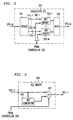
- FIG. 3 shows, in simplified block diagram form, details of an exemplary squelcher (S) unit.
- the STS-M digital signal is supplied to demultiplexer (DEMUX) 301 where it is demultiplexed into its constituent M STS-1 digital signals 301-1 through 302-M.
- the M STS-1 digital signals are supplied on a one-to-one basis to AIS insert units 303-1 through 303-M.
- AIS insert units 303-1 through 303-M under control of controller 205, insert the AIS in the STS-1 digital signals included in the communications circuits, i.e., STS-M digital signals, to be squelched. Details of AIS insert units 303 are shown in FIG. 4 and described below.
- the M STS-1 digital signals are multiplexed in multiplexer (MUX) 304 to yield the desired STS-M digital signal.
- MUX multiplexer
- FIG. 4 shows, in simplified block diagram form, details of AIS insert units 303. Specifically, shown is a STS-1 digital signal being supplied to AIS generator 401 and to one input of 2:1 selector 402. AIS generator 401 operates to insert AIS in the STS-1 digital signal. As indicated in the technical advisory TA-NWT-000253, the STS path AIS is an all ones (1's) signal in the STS-1 overhead bytes H1, H2 and H3 and the bytes of the entire STS SPE (synchronous payload envelope). Selector 402 selects as an output, under control of controller 205, either the incoming STS-1 digital signal or the STS-1 digital signal with AIS inserted from AIS generator 401.
- FIG. 5 is a table including the identification (ID) of ring nodes 110 through 115 for bidirectional line-switched ring 100.
- the ring node IDs are stored in a look-up table which is provisioned via 228 in memory of controller 205 (FIG. 2).
- FIG. 6 is illustrative of a table including the identification of all the active communications circuits in a ring node, in this example, ring node 111 for a counter-clockwise orientation of nodes 110 through 115.
- the active communications circuits include those being added, being dropped or passing through ring node 111 and, additionally, those terminated in an interworking ring node.
- the table including the IDs of the active communications circuits in the ring node are provisioned via 228 in a look-up table in memory of controller 205. Shown in the table of FIG.
- An interworking communications circuit is one which has terminations in both bidirectional-line switched ring 100 and bidirectional line-switched ring 101.
- a communications circuit terminated in its primary interworking ring node 112 in shared node 130 is shown as being broadcast to its secondary interworking ring node 114 in shared node 131 and identified in the provisioning as being a ring interworking communications circuit.
- the communications circuit ID table of FIG. 6 shows that STS-M(a) enters ring 100 at ring node 110 and exits ring 100 at ring node 111, and is not a ring interworking communications circuit.
- STS-M(b) enters ring 100 at ring node 111 and exits at ring nodes 113 and is not a ring interworking communications circuit.
- STS-M(c) enters ring 100 at ring node 110 and normally exits at ring node 112, and is a interworking communications circuit.
- interworking ring node 112 fails, the communications circuits terminated in it will not be squelched in adjacent ring nodes 111 and 113, but will be supplied via loop-back-switching to its secondary interworking ring node 114. Provided, however, that neither the secondary interworking ring node 114 for the communications circuit nor the ring node terminating the communications circuit in ring 100 has also failed.
- STS-M(d) enters ring 100 at ring node 111 and exits at ring node 115.
- the ring nodes designated A terminations are considered entry points and the ring nodes designated Z terminations are considered exit points, it will be apparent that the individual communications circuits may be duplex circuits having entry and exit points at each such node.
- FIG. 7 is a flow chart illustrating the operation of controller 205 in controlling the operation of the ring nodes in order to effect the deterministic squelching of communications circuits and the selective provisioning of the secondary duplex communications circuit connection(s) to secondary interworking ring node 114 for communications circuits terminated in their failed primary interworking ring node 112.
- the process is entered via step 701.
- operational block 702 causes the K bytes of an incoming OC-N signal to be observed and processes the ring node IDs therein.
- conditional branch point 703 tests to determine if the processed ring node IDs indicate that one or more ring nodes have failed.
- a ring node failure is defined as to include node equipment failure and so-called node isolation failure caused by fiber cuts and the like. Specific examples of failure conditions are discussed below.
- operational block 704 causes the usual bidirectional ring bridging and switching to be effected. Thereafter, the process is ended via step 705. If the processed ring node IDs indicate a multiple ring node failure, operational block 706 causes the failed ring node IDs to be obtained from the ring node ID look-up table in memory.
- control is passed to operational block 707 which causes the identity (ID) of the affected communications circuits to be obtained from the communications circuit ID look-up table in memory. If step 703 indicates a single ring node failure, the failed ring node ID is already known and control is passed directly to step 707.
- operational block 708 causes the appropriate ones of squelchers (S) 204, 210, 217 and 219 (FIG. 2), in this example, to squelch those identified communications circuits in the ring node. As indicated above, all communications circuits active in this ring node that are terminated in a failed ring node are squelched.
- a ring interworking communications circuit is treated, for the purpose of squelching, just like a broadcast communications circuit from its termination in bidirectional line-switched ring 100 to its primary shared node and secondary shared node.
- Operational block 704 causes the communications circuits not terminated in the failed ring node(s) to be bridged and switched to "heal" the ring. Thereafter, the process is ended in step 705.
- FIG. 8 illustrates in simplified form a "normal" ring interworking communications circuit connection in bidirectional line-switched ring 100.
- the communications circuit connection is between ring node 110, the A termination, and its primary interworking ring node 112.
- T A one portion of the duplex communications circuit enters ring 100 at ring node 110 and is supplied in the service bandwidth of transmission path 116 through ring node 111 to its primary interworking ring node 112.
- the received portion of the communications circuit is normally handed-off as Rp in ring node 112.
- the received portion is also passed along through ring node 113 to also be received at its secondary interworking ring node 114 as R S .
- T P another portion of the duplex communications circuit normally enters ring 100 at its primary interworking ring node 112 and is selected to be supplied to the service bandwidth of transmission path 117.
- this portion of the communications circuit is passed through ring node 111 and received as R A at ring node 110.
- this portion of the communications circuit is supplied as T s from secondary interworking ring node 114 in the service bandwidth of transmission path 117 through ring node 113 and is available as a candidate to be selected for transmission at primary interworking ring node 112.
- the communications circuit T s is also dropped at primary ring node 112 as unidirectional communications circuit R' P .
- communications circuit R' P is available so that the lower level digital signals may be obtained for comparison and selection.
- this selection of T S occurs if the hand-off link fails in primary interworking ring node 112.
- ring node 112 can be provisioned to normally select the communications circuit T S from ring node 114. It is noted that the communications circuit is being dual fed to bidirectional line-switched ring 100 from path-switched ring 101 via ring nodes 120 and 125.
- the hand-off link fails in the primary interworking ring node 112 for a communications circuit, the affected communications circuit or portion of it is being broadcast along to be obtained in the secondary interworking ring node 114 for the communication circuit.
- the receive (R P ) portion of the hand-off link fails in primary interworking ring node 112
- it is passed along via broadcast element 206 and 3:1 selector 207 (FIG. 2) and selected to be handed-off as R S in secondary interworking ring node 114.
- controller 205 in ring node 112 causes 3:1 selector 209 (FIG. 2) to select the transmit (T S ) portion of the communications circuit from secondary interworking ring node 114.
- FIG. 9 shows, in simplified block diagram form, a digital cross-connect system (DCS) including apparatus embodying an aspect of the invention.
- DCS digital cross-connect system
- DEMUX 901 demultiplexes the STS-1 signal to obtain the VT signals in known fashion.
- the VT signals are supplied to time slot interchanger (TSI) 902 where they are groomed under control of controller 903. Then, the groomed VT signals are supplied on a one-to-one basis to 2:1 selectors 904-1 through 904-Y, where Y is the number of VT signals being transported by the STS-1 signal.
- TSI time slot interchanger
- a corresponding inter-ring groomed STS-1 signal (R') supplied from secondary interworking ring node 114 in shared node 131 is demultiplexed in demultiplexer (DEMUX) 905 to obtain VT signals which correspond on a one-to-one basis with the VT signals being supplied to selectors 904 from TSI 902.
- the VT signals from DEMUX 905 are supplied on a one-to-one basis to other inputs of selectors 905-1 through 905-Y.
- Controller 903 evaluates the VT signals on a pair-wise basis, in this example, in both DEMUX 901 and DEMUX 905, to determine the best VT signal in each pair and, then, causes selectors 904 to select the best VT signals.
- the evaluation may include monitoring the VT signals for loss of signal, AIS and/or bit error rate.
- the selection of the VT signals is such that the corrupted and/or failed VT signals are not selected.
- the selected VT signals are combined via multiplexer (MUX) 906 to obtain the desired inter-ring groomed STS-1 signal (T).
- MUX multiplexer
- FIG. 10 shows, in simplified block diagram form another arrangement embodying an aspect of the invention. Specifically, shown are DCS 1001 and selector unit 1002 which form inter-ring grooming apparatus 132. It is noted that for brevity and clarity of description only one direction of signal transmission is shown and only one digital signal will be considered. It will be apparent to those skilled in the art that there is a similar opposite direction of transmission and that a relatively large number of digital signals would normally be groomed by such a DCS. Again, in this example, a SONET STS-1 digital signal is being groomed at the lower VT digital signal level.
- DCS 1001 includes controller 1003, DEMUX 1004, TSI 1005 and MUX 1006 and operates in known fashion to groom STS-1 signals at the VT signal level.
- an STS-1 signal (T') being supplied from ring node 120 (FIG. 1) in bidirectional line-switched ring 101 to DCS 1001 and therein to DEMUX 1004.
- DEMUX 1004 demultiplexes the STS-1 signal to obtain the VT signals in known fashion.
- the VT signals are supplied to TSI 1005 where they are groomed under control of controller 1003.
- the groomed VT signals are supplied to MUX 1006 where they are combined into a groomed STS-1 signal (T").
- the groomed STS-1 signal T" is supplied to selector unit 1002 and therein to DEMUX 1007.
- DEMUX 1007 demultiplexes the groomed STS-1 signal T" to obtain the VT signals.
- the VT signals are supplied on a one-to-one basis to first inputs of 2:1 selectors 1008-1 through 1008-Y, where Y is the number of VT signals being transported by the STS-1 signal.
- a corresponding inter-ring groomed STS-1 signal (R') supplied from secondary interworking ring node 114 in shared node 131 is demultiplexed in DEMUX 1009 to obtain VT signals which correspond on a one-to-one basis with the VT signals being supplied to selectors 1008 from DEMUX 1007.
- the VT signals from DEMUX 1009 are supplied on a one-to-one basis to second inputs of selectors 1008-1 through 1008-Y.
- Controller 1010 evaluates the VT signals on a pair-wise basis, in this example, in both DEMUX 1007 and DEMUX 1009, to determine the best VT signal in each pair and, then, causes selectors 1008 to select the best VT signals.
- the evaluation may include monitoring the VT signals for loss of signal, coding violations and the like.
- the selection of the VT signals is such that the corrupted and/or failed VT signals are not selected. Thereafter, the selected VT signals are combined via MUX 1011 to obtain the desired inter-ring groomed STS-1 signal (T).
- FIG. 11 illustrates the ring interworking communications circuit transmission in ring 100 when a failure arises in the hand-off link in its primary interworking node 112.
- the same "good" transmit signal T S from secondary interworking ring node 114 is selected in primary interworking ring node 112 to be supplied in the service bandwidth on transmission path 117 to ring node 110.
- Primary interworking ring node 112 can still select the received portion (Rp) of the communications circuit from ring node 110.
- secondary interworking ring node 114 selects the received signal (R S ), which is passed-on from primary interworking ring node 112.
- Each of ring nodes 120 through 125 comprises an add-drop multiplexer (ADM).
- ADM add-drop multiplexer
- Such add-drop multiplexer arrangements are known.
- SONET ADM SONET ADD-DROP Multiplex Equipment
- GENERIC CRITERIA TR-TSY-000496, Issue 2, September 1989, Supplement 1, September 1991, Bell Communications Research.
- the ADM operates to pass signals through the ring node, to add signals at the ring node and to drop signals at the ring node.
- DCS 132 includes or interfaces with the evaluation, selection and multiplexing apparatus as shown in FIG. 9 or FIG. 10 and described above.
- FIG. 12 shows, in simplified block diagram form, details of ring nodes 120 through 125.
- a west (W)-to-east (E) digital signal transmission direction is assumed in the bandwidth on transmission path 128. It will be apparent that operation of the ring node and the ADM therein would be similar for an east (E) - to - west (W) digital signal transmission direction in the bandwidth on transmission path 129.
- transmission path 128 entering the ring node and supplying an OC-N SONET optical signal to receiver 1201, where N could be, for example, 3, 12 or 48.
- Receiver 1201 includes an optical/electrical (O/E) interface 1202 and a demultiplexer (DEMUX) 1203, which yields at least one (1) STS-M SONET digital signal.
- O/E interfaces and demultiplexers are known.
- M is assumed to be three (3) and N is greater than M.
- the STS-M signal output from DEMUX 1203 is supplied to broadcast element 1206.
- a broadcast element replicates the STS-M signal supplied to it and supplies the replicated signals as a plurality of individual outputs. Such broadcast elements are known.
- Broadcast element 1206 generates two identical STS-M signals and supplies one STS-M signal to an input of 2:1 selector 1207 and another STS-M signal to an input of 2:1 selector 1208.
- An STS-M signal output from 2:1 selector 1207 is supplied to transmitter 1211 and, therein, to multiplexer (MUX) 1212.
- the output of MUX 1212 is an electrical OC-N digital signal, which is interfaced to transmission path 128 via electrical/optical (E/O) interface 1213.
- E/O electrical/optical
- Such multiplexers (MUXs) and electrical/optical (E/O) interfaces are well known.
- an OC-N optical signal is supplied via transmission path 129 to receiver 1214 and, therein, to optical/electrical (O/E) interface 1215.
- demultiplexer (DEMUX) 1216 yields a STS-M signal which is supplied to broadcast element 1218.
- Broadcast element 1218 replicates the STS-M signal into a plurality of identical STS-M signals, in this example, three (3).
- One STS-M signal is supplied to an input of 2:1 selector 1208, a second STS-M signal is supplied to an input of 2:1 selector 1209 and a third STS-M signal is supplied to interface 1231.
- An output from 2:1 selector 1209 is supplied to transmitter 1220.
- multiplexer (MUX) 1229 multiplexes the STS-M into an electrical OC-N and, then, electrical/optical (E/O) interface 1222 supplies the optical OC-N signal to transmission path 129.
- broadcast element 1218 supplies the secondary communications circuits from the additional shared node as candidates for through circuits and also drops the secondary communications circuits via interface 1231 under control of controller 1205.
- the communications circuits are SONET STS-3 digital signals
- interface 1231 and interface 1224 drop SONET STS-1 digital signals.
- STS-1 digital signals are combined in the interfaces to form STS-3 digital signals, in known fashion.
- selector 1208 selects on a STS-1 level. To this end, the STS-3 digital signals are demultiplexed in selector 1208 to obtain the three STS-1 digital signals, the STS-1 signals are selected and then multiplexed back into a STS-3 signal, which is supplied to interface 1224.
- Selector 1209 is provisioned under control of controller 1205 to normally select the STS-M signal being supplied from interface 1224.
- Controller 1205 operates to control selection of the STS-3 signals via selectors 1207, 1208 and 1209 based on their health. Controller 1205 communicates with demultiplexers 1203 and 1216 and multiplexers 1212 and 1221 via bus 1223, with interface 1224 via bus 1227, with interface 1231 via bus 1232, with selector 1207 via bus 1234, with selector 1209 via bus 1225 and with selector 1208 via bus 1235. Specifically, controller 1205 monitors the incoming digital signals to determine loss-of-signal, alarm conditions, presence of alarm indication signal (AIS) and the like.
- AIS alarm indication signal
- controller 1205 When operating as a primary interworking ring node, controller 1205 controls the dropping, via interface 1231, of the secondary communications circuits being supplied from the secondary ring node of shared node 131 (FIG. 1) and the dual feeding on an STS-M signal from interface 1224 via broadcast element 1226 and selectors 1207 and 1209.
- controller 1205 controls the revertive biasing of selector 1207 to normally select the STS-M signal from broadcast element 1206, i.e., from the primary interworking ring node to be supplied as an output on transmission path 128.
- controller 1205 controls selector 1207 to select the secondary communications circuit (STS-M) being supplied from interface 1224 via broadcast element 1226.
- STS-M secondary communications circuit
- selector 1207 automatically reverts back to selecting it under control of controller 1205.
- the health of the communications circuit Tp from the primary node and the communications circuit T s in the secondary node is monitored to determine if selector 1207 will make a real time switch to select T s .
- Interface 1224 is employed to interface, in this example, to the particular inter-ring grooming apparatus being employed. As indicated above, in this example both interface 1224 and interface 1231 between STS-3 digital signals to STS-1 digital signals, in known fashion. Specifically, an STS-3 digital signal to be dropped at the ring node is supplied to interface 1224 via 2:1 selector 1208, under control of controller 1205, from either broadcast element 1206 or broadcast element 1218. When operating as a primary interworking ring node, selector 1208 normally is controlled to select the STS-3 signal being supplied from the west (W) via broadcast element 1206 and when operating as a secondary interworking ring node selector 1208 is controlled to select the STS-3 signal being supplied from the east (E) via broadcast element 1218.
- W west
- E east
- This STS-3 signal is demultiplexed in interface 1224 and supplied as three (3) STS-1 signals (R) to circuit path 1230.
- an STS-3 secondary communications circuit being supplied, via broadcast element 1218, to interface 1231 is demultiplexed therein, under control of controller 1205, and supplied as three (3) STS-1 signals (R') to circuit path 1233.
- a signal (T) to be added at the ring node is supplied to interface 1224 where it is converted to the STS-M digital signal format, if necessary.
- the STS-M digital signal is then supplied to broadcast element 1226 where it is replicated.
- the replicated STS-M digital signals are supplied by broadcast element 1226 to an input of 2:1 selector 1207 and an input of 2:1 selector 1209.
- 2:1 selectors 1207 and 1209 under control of controller 1205, dual feed the signal being added for transmission in the bandwidth on both transmission path 128 and transmission path 129.
- provisioning at termination ring node 122 is as follows:
- Controller 1205 controls and monitors the status of interface 1224 and the digital signals being supplied thereto via bus 1227 and controls and monitors interface 1231 via bus 1232. Specifically, controller 1205 monitors interface 1224 for loss-of-signal, coding violations and the like.
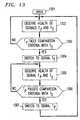
- FIG. 13 illustrates in flow chart form the operation in secondary ring node 125 of selector 1207 (FIG. 12) in effecting the revertive selection between new primary communications circuit Tp from primary ring node 120 and secondary communications circuit T S from ring node 125 during normal and abnormal conditions of the new primary communications circuit.
- the operation is entered vi step 1301.
- step 1302 causes the health to be obversed of signals Tp and T S .
- Step 1303 tests to determine if signal Tp fails the comparison criteria with T S . If the test result is NO, T P is normal, and control is returned to step 1302 and steps 1302 and 1303 are iterated.
- step 1303 If the test result in step 1303 is YES, Tp is abnormal, and step 1304 causes a switch to signal T S . Then, step 1305 causes the health to be observed of signals T p and T S . Step 1306 tests to determine if signal T p passes the comparison criteria with T S . If the test result is NO, Tp continues to be abnormal, and control is returned to step 1305 and steps 1305 and 1306 are iterated. If the test result in step 1306 is YES, T P has returned to normal, and step 1307 causes a switch, i.e., an automatic reversion, to signal Tp and control is returned to step 1302. Thereafter, the process is repeated.
- T P has returned to normal
- step 1307 causes a switch, i.e., an automatic reversion, to signal Tp and control is returned to step 1302. Thereafter, the process is repeated.
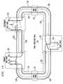
- FIG. 14 illustrates in simplified form a "normal" ring interworking communications circuit connection in path-switched ring 101.
- the communications circuit connection is between ring node 122, the A termination, and its primary interworking ring node 120 and its secondary interworking node 125.
- one portion (T A ) of the duplex communications circuit enters ring 101 at ring node 122 and is supplied in the bandwidth of transmission path 128 through ring node 121 to its primary interworking ring node 120 and is supplied in the bandwidth of transmission path 129 through ring node 123 to its secondary interworking ring node 125.
- the transmit portion, i.e., T A of the communications circuit is normally handed-off as Rp in ring node 120 and as R S in ring node 125.
- another portion (T P ) of the duplex communications circuit normally enters ring 101 at its primary interworking ring node 120 and is supplied to the bandwidth of transmission path 129 and to the bandwidth of transmission path 128.
- T P is supplied in transmission path 128 to secondary interworking ring node 125.
- T P is normally selected and supplied through ring node 123 to ring node 122 where it is also received as R A .
- this portion of the communications circuit is passed through ring node 121 and received as R A at ring node 122.
- Ring node 122 normally selects R A from transmission path 129. Additionally, this portion of the communications circuit is supplied as T S from secondary interworking ring node 125 in the bandwidth of transmission path 129 and and is dropped at primary ring node 120 as unidirectional communications circuit R' P . Then communications circuit R' P is available so that the lower level digital signals may be obtained for comparison and selection. Secondary interworking ring node 125
- FIG. 15 illustrates the ring interworking communications circuit transmission in ring 101 when a failure arises in the hand-off link in its primary interworking node 120.
- the same "good" transmit signal T S is selected in secondary interworking ring node 125 and supplied in the bandwidth on transmission path 128 to ring node 122.
- Ring node 122 selects the transmit signal T S from transmission path 128 as receive signal R A .
- Primary interworking ring node 120 can still select the received portion (R P ) of the communications circuit from ring node 122.
- secondary interworking ring node 125 selects the received signal (R S ), which is being supplied on transmission path 129 from ring node 122.
Claims (12)
- Kommunikationssystem, umfassend:ein bidirektionales leitungsgeschaltetes Ringübertragungssystem (100), das einen ersten und einen zweiten Kommunikationsweg zum Transportieren von Kommunikationskreisen in entgegengesetzten Richtungen um den Ring herum aufweist;ein weggeschaltetes Ringübertragungssystem (101), das einen ersten und einen zweiten Kommunikationsweg zum Transportieren von Kommunikationskreisen in entgegengesetzten Richtungen um den Ring herum aufweist;wobei jeder Kommunikationskreis eine erste Übertragungsgeschwindigkeit hat und mehrere digitale Signale aufweist, die jeweils eine niedrigere Übertragungsgeschwindigkeit als die erste Übertragungsgeschwindigkeit haben;
einen ersten Interworking-Knoten (130), der jeweils einen ersten Ringknoten (112, 120) in jedem bidirektionalen leitungsgeschalteten Ringübertragungssystem und dem weggeschalteten Ringübertragungssystem und eine zwischen den ersten Ringknoten zwischengeschaltete erste Inter-Ring-Grooming-Vorrichtung (132) zum Anordnen der digitalen Signale mit niedrigerer Übertragungsgeschwindigkeit zu primären Kommunikationskreisen mit der ersten Übertragungsgeschwindigkeit aufweist;
einen zweiten Interworking-Knoten (131), der jeweils einen zweiten Ringknoten (114, 125) in dem bidirektionalen leitungsgeschalteten Ringübertragungssystem und dem weggeschalteten Ringübertragungssystem und eine zwischen den zweiten Ringknoten zwischengeschaltete zweite Inter-Ring-Grooming-Vorrichtung (133) zum Anordnen der digitalen Signale mit niedrigerer Übertragungsgeschwindigkeit zu primären Kommunikationskreisen mit der ersten Übertragungsgeschwindigkeit aufweist, wobei der zweite Ringknoten (114) in dem bidirektionalen leitungsgeschalteten Ringübertragungssystem so beschaffen ist, dass er wenigstens einen sekundären, einem Inter-Ring-Grooming unterzogenen Kommunikationskreis dem ersten Ringknoten (112) in dem bidirektionalen leitungsgeschalteten Ringübertragungssystem zuführt, wobei der sekundäre Kommunikationskreis einem primären, einem Inter-Ring-Grooming unterzogenen Kommunikationskreis entspricht, der von der ersten Inter-Ring-Grooming-Vorrichtung (132) dem ersten Ringknoten (112) in dem bidirektionalen leitungsgeschalteten Ringübertragungssystem zugeführt wird, wobei einer der Interworking-Knoten ein primärer Interworking-Knoten ist und der andere der Interworking-Knoten ein sekundärer Interworking-Knoten ist, gekennzeichnet durch
Mittel, die mit dem ersten Ringknoten in dem bidirektionalen leitungsgeschalteten Ringübertragungssystem verknüpft sind, welche Mittel (239, 905) zum Demultiplexieren des wenigstens einen sekundären Kommunikationskreises aufweisen, um die mehreren digitalen Signale mit niedrigerer Übertragungsgeschwindigkeit zu erhalten,
Mittel zum Bewerten (904-1...Y) der digitalen Signale mit niedrigerer Übertragungsgeschwindigkeit von dem sekundären Kommunikationskreis auf einer paarweisen Basis mit entsprechenden digitalen Signalen mit niedrigerer Übertragungsgeschwindigkeit des entsprechenden primären Kommunikationskreises gemäß vorgeschriebenen Kriterien, um das Signal mit niedrigerer Übertragungsgeschwindigkeit in jedem Paar zu bestimmen, welches am wenigsten verfälscht ist,
Mittel (903), die auf die Ergebnisse des Bewertens reagieren, zum Auswählen des am wenigsten verfälschten Signals von den digitalen Signalen mit niedrigerer Übertragungsgeschwindigkeit in den Paaren,
Mittel zum Kombinieren (906, 224) der ausgewählten digitalen Signale mit niedrigerer Übertragungsgeschwindigkeit zu einem neuen primären Kommunikationskreis, und
erste Mittel zum normalen Einfügen (226) des neuen primären Kommunikationskreises in einen Kommunikationsweg in dem bidirektionalen leitungsgeschalteten Ringübertragungssystem,
wobei die Bewertung und Auswahl der digitalen Signale mit niedrigerer Übertragungsgeschwindigkeit nur in dem primären Ringknoten von den Interworking-Ringknoten in dem bidirektionalen leitungsgeschalteten Ringübertragungssystem durchgeführt wird, wobei der zweite Ringknoten in dem weggeschalteten Ringübertragungssystem so beschaffen ist, dass er wenigstens einen sekundären, einem Inter-Ring-Grooming unterzogenen Kommunikationskreis einem ersten Ringknoten in dem weggeschalteten Ringübertragungssystem zuführt, wobei der sekundäre Kommunikationskreis einem primären, einem Inter-Ring-Grooming unterzogenen Kommunikationskreis entspricht, der von der ersten Inter-Ring-Grooming-Vorrichtung zugeführt wird;
Mittel, die mit dem ersten Ringknoten in dem weggeschalteten Ringübertragungssystem verknüpft sind, welche aufweisen
Mittel zum Demultiplexieren (1231, 905) des wenigstens einen sekundären Kommunikationskreises, um die mehreren digitalen Signale mit niedrigerer Übertragungsgeschwindigkeit zu erhalten,
Mittel zum Bewerten (904-1...Y) der digitalen Signale mit niedrigerer Übertragungsgeschwindigkeit von dem sekundären Kommunikationskreis auf einer paarweisen Basis mit entsprechenden digitalen Signalen mit niedrigerer Übertragungsgeschwindigkeit des entsprechenden primären Kommunikationskreises gemäß vorgeschriebenen Kriterien, um das Signal mit niedrigerer Übertragungsgeschwindigkeit in jedem Paar zu bestimmen, welches am wenigsten verfälscht ist,
Mittel (903), die auf die Ergebnisse des Bewertens reagieren, zum Auswählen des am wenigsten verfälschten Signals von den digitalen Signalen mit niedrigerer Übertragungsgeschwindigkeit in den Paaren,
Mittel zum Kombinieren (906, 1224) der ausgewählten digitalen Signale mit niedrigerer Übertragungsgeschwindigkeit zu einem neuen primären Kommunikationskreis, und
zweite Mittel (1226) zum Einfügen des neuen primären Kommunikationskreises in den ersten und zweiten Kommunikationsweg in dem weggeschalteten Ringübertragungssystem; und
erste Mittel (1207, 1209) in dem zweiten Ringknoten in dem weggeschalteten Ringübertragungssystem zum normalen Auswählen des neuen primären Kommunikationskreises aus dem ersten Ringknoten dafür, dass er auf einem Kommunikationsweg zu durchlaufen ist,
wobei die Bewertung und Auswahl der digitalen Signale mit niedrigerer Übertragungsgeschwindigkeit nur in dem primären Ringknoten von den Interworking-Ringknoten in dem weggeschalteten Ringübertragungssystem durchgeführt wird. - System nach Anspruch 1, wobei das erste Mittel zum Einfügen zweite steuerbare Auswahlmittel zum Auswählen des neuen primären Kommunikationskreises unter normalen Bedingungen und zum Auswählen des entsprechenden sekundären Kommunikationskreises unter anormalen Bedingungen aufweist.
- System nach Anspruch 2, wobei das erste Mittel zum Einfügen ferner Mittel zum Steuern der zweiten Mittel zum Auswählen aufweist, um bei einer Rückkehr von den anormalen Bedingungen zu den normalen Bedingungen automatisch zum Auswählen des neuen primären Kommunikationskreises zurückzukehren.
- System nach Anspruch 3, wobei die Kommunikationskreise von dem bidirektionalen leitungsgeschalteten Ringübertragungssystem jeweils sowohl der ersten als auch der zweiten Inter-Ring-Grooming-Vorrichtung zum Inter-Ring-Grooming der digitalen Signale mit niedrigerer Übertragungsgeschwindigkeit in ihnen zugeführt werden.
- System nach Anspruch 1, wobei das erste Mittel zum Einfügen steuerbare Auswahlmittel zum Auswählen des neuen primären Kommunikationskreises, der von dem primären Ringknoten zugeführt wird, unter normalen Bedingungen und zum Auswählen des entsprechenden sekundären Kommunikationskreises, der von dem sekundären Ringknoten zugeführt wird, unter anormalen Bedingungen aufweist.
- System nach Anspruch 5, wobei das erste Mittel zum Einfügen ferner Mittel zum Steuern der Mittel zum Auswählen aufweist, um bei einer Rückkehr von den anormalen Bedingungen zu den normalen Bedingungen automatisch zum Auswählen des neuen primären Kommunikationskreises zurückzukehren.
- System nach Anspruch 6, wobei das zweite Mittel zum Einfügen Mittel zum zweifachen Einspeisen des neuen primären Kommunikationskreises sowohl in den ersten als auch in den zweiten Kommunikationsweg in dem weggeschalteten Ringübertragungssystem aufweist.
- System nach Anspruch 6, wobei Kommunikationskreise von dem weggeschalteten Ringübertragungssystem jeweils sowohl der ersten als auch der zweiten Inter-Ring-Grooming-Vorrichtung zum Inter-Ring-Grooming der digitalen Signale mit niedrigerer Übertragungsgeschwindigkeit in ihnen zugeführt werden.
- System nach Anspruch 7, wobei der zweite Ringknoten in dem weggeschalteten Ringübertragungssystem Mittel zum zweifachen Einspeisen des sekundären Kommunikationskreises in dem weggeschalteten Ringübertragungssystem in den ersten Ringknoten in dem weggeschalteten Ringübertragungssystem und in das erste Mittel zum Einfügen aufweist.
- System nach Anspruch 3 oder 7, wobei die Kommunikationskreise aus digitalen Signalen vom Typ SONET STS bestehen und die digitalen Signale mit niedrigerer Übertragungsgeschwindigkeit digitale Signale vom Typ SONET VT sind.
- System nach Anspruch 3 oder 7, wobei die Kommunikationskreise aus digitalen Signalen vom Typ DS3 bestehen und die digitalen Signale mit niedrigerer Übertragungsgeschwindigkeit digitale Signale DS1 sind.
- System nach Anspruch 3 oder 7, wobei die Kommunikationskreise aus digitalen Signalen vom Typ SDH STM bestehen und die digitalen Signale mit niedrigerer Übertragungsgeschwindigkeit digitale Signale SDH VC von niedrigerer Ordnung sind.
Applications Claiming Priority (2)
| Application Number | Priority Date | Filing Date | Title |
|---|---|---|---|
| US141141 | 1988-01-06 | ||
| US08/141,141 US5394389A (en) | 1993-10-22 | 1993-10-22 | Ring interworking between bidirectional line-switched ring transmission systems and path-switched ring transmission systems |
Publications (3)
| Publication Number | Publication Date |
|---|---|
| EP0654922A2 EP0654922A2 (de) | 1995-05-24 |
| EP0654922A3 EP0654922A3 (de) | 1998-07-08 |
| EP0654922B1 true EP0654922B1 (de) | 2006-07-19 |
Family
ID=22494347
Family Applications (1)
| Application Number | Title | Priority Date | Filing Date |
|---|---|---|---|
| EP94307455A Expired - Lifetime EP0654922B1 (de) | 1993-10-22 | 1994-10-12 | Kommunikationssystem bestehend aus miteinander verbundenen, leitungsgeschalteten und weggeschalteten Ringübertragungssystemen |
Country Status (5)
| Country | Link |
|---|---|
| US (1) | US5394389A (de) |
| EP (1) | EP0654922B1 (de) |
| JP (1) | JP3126605B2 (de) |
| CA (1) | CA2130066C (de) |
| DE (1) | DE69434795T2 (de) |
Families Citing this family (44)
| Publication number | Priority date | Publication date | Assignee | Title |
|---|---|---|---|---|
| JP2784080B2 (ja) | 1990-05-09 | 1998-08-06 | 富士通株式会社 | リングネットワーク及びその障害復旧方法並びにリングネットワークに用いられるノード |
| JP2541107B2 (ja) * | 1993-06-30 | 1996-10-09 | 日本電気株式会社 | クロスコネクト用インタフェ―スおよび装置 |
| US5864414A (en) * | 1994-01-26 | 1999-01-26 | British Telecommunications Public Limited Company | WDM network with control wavelength |
| US5742605A (en) * | 1994-02-28 | 1998-04-21 | Sprint Communications Co., L.P. | Synchronous optical network using a ring architecture |
| JP3561848B2 (ja) * | 1994-03-01 | 2004-09-02 | 富士通株式会社 | 伝送装置及び冗長構成切替方法 |
| JPH07264229A (ja) * | 1994-03-18 | 1995-10-13 | Fujitsu Ltd | 仮想リング構成システム |
| JPH07264227A (ja) * | 1994-03-18 | 1995-10-13 | Fujitsu Ltd | 複合リング状ネットワーク制御方式 |
| JPH07264223A (ja) * | 1994-03-18 | 1995-10-13 | Fujitsu Ltd | ネットワークの信号救済方法および装置 |
| JP3259126B2 (ja) * | 1995-09-26 | 2002-02-25 | 富士通株式会社 | リング伝送システム及び該システムのスケルチ方法 |
| US6256292B1 (en) * | 1996-07-11 | 2001-07-03 | Nortel Networks Corporation | Self-healing line switched ring for ATM traffic |
| DE19745021B4 (de) * | 1996-10-29 | 2008-08-28 | Keymile Ag | Netzwerk für paketorientierten Datenverkehr |
| US6111859A (en) * | 1997-01-16 | 2000-08-29 | Advanced Micro Devices, Inc. | Data transfer network on a computer chip utilizing combined bus and ring topologies |
| US6047002A (en) * | 1997-01-16 | 2000-04-04 | Advanced Micro Devices, Inc. | Communication traffic circle system and method for performing packet conversion and routing between different packet formats including an instruction field |
| US6247161B1 (en) | 1997-01-16 | 2001-06-12 | Advanced Micro Devices, Inc. | Dynamically configured on-chip communications paths based on statistical analysis |
| US6266797B1 (en) | 1997-01-16 | 2001-07-24 | Advanced Micro Devices, Inc. | Data transfer network on a computer chip using a re-configurable path multiple ring topology |
| US6018782A (en) * | 1997-07-14 | 2000-01-25 | Advanced Micro Devices, Inc. | Flexible buffering scheme for inter-module on-chip communications |
| US5908468A (en) * | 1997-10-24 | 1999-06-01 | Advanced Micro Devices, Inc. | Data transfer network on a chip utilizing a multiple traffic circle topology |
| US5909175A (en) * | 1997-02-28 | 1999-06-01 | Fujitsu Limited | Connection switching circuit for ring system |
| US5974487A (en) * | 1997-07-14 | 1999-10-26 | Advanced Micro Devices, Inc. | Data transfer network on a chip utilizing a mesh of rings topology |
| US6233221B1 (en) * | 1998-02-20 | 2001-05-15 | Adc Telecommunications, Inc. | System and method for a ring network with virtual path connections |
| WO1999043184A1 (en) | 1998-02-20 | 1999-08-26 | Adc Telecommunications, Inc. | Protection switching of virtual connections |
| US6940810B1 (en) | 1998-02-20 | 2005-09-06 | Adc Telecommunications, Inc. | Protection switching of virtual connections at the data link layer |
| US6407983B1 (en) | 1998-02-20 | 2002-06-18 | Adc Telecommunications, Inc. | Circuit and method for shaping traffic in a virtual connection network |
| US6216166B1 (en) | 1998-02-20 | 2001-04-10 | Adc Telecommunications, Inc. | Shared media communications in a virtual connection network |
| US6757247B1 (en) | 1998-02-20 | 2004-06-29 | Adc Telecommunications, Inc. | Circuit and method for controlling virtual connections in a ring network |
| US6606297B1 (en) * | 1998-05-29 | 2003-08-12 | Tellabs Operations, Inc. | Bi-directional ring network having minimum spare bandwidth allocation and corresponding connection admission control |
| US6545977B2 (en) * | 1998-06-03 | 2003-04-08 | Lucent Technologies Inc. | Methods and apparatus for routing signals in a ring network |
| US6560240B1 (en) | 1998-09-04 | 2003-05-06 | Advanced Micro Devices, Inc. | System-on-a-chip with variable clock rate |
| US6724772B1 (en) | 1998-09-04 | 2004-04-20 | Advanced Micro Devices, Inc. | System-on-a-chip with variable bandwidth |
| US6349092B1 (en) * | 1998-11-16 | 2002-02-19 | Cisco Systems, Inc. | BLSR node extension |
| US6301254B1 (en) | 1999-03-15 | 2001-10-09 | Tellabs Operations, Inc. | Virtual path ring protection method and apparatus |
| US6807190B1 (en) * | 1999-05-25 | 2004-10-19 | Lucent Technologies Inc. | Survivable distribution of broadcast signals in loopback rings |
| US6667981B1 (en) * | 1999-06-30 | 2003-12-23 | Worldcom, Inc. | Method of partitioning traffic and placing add/drop multiplexers in a stacked ring network |
| JP3780153B2 (ja) * | 1999-10-25 | 2006-05-31 | 富士通株式会社 | リング伝送システム用光伝送装置及びリング伝送システム用光伝送方法 |
| IT1319278B1 (it) * | 2000-05-26 | 2003-10-10 | Cit Alcatel | Interconnessione tra reti ad anello per telecomunicazioni tipoms-spring ed sncp. |
| US20030142678A1 (en) * | 2000-07-28 | 2003-07-31 | Chan Eric L. | Virtual path ring protection method and apparatus |
| US6744769B1 (en) | 2000-10-19 | 2004-06-01 | Nortel Networks Limited | Path provisioning on ring-based networks |
| EP1209834B1 (de) * | 2000-11-28 | 2017-11-08 | Kabushiki Kaisha Toshiba | Ringverbindungssystem, Knotenausrüstung , Netzwerkmanagement-Ausrüstung und Verfahren zur Pfadfestlegung |
| US6731830B2 (en) | 2001-01-05 | 2004-05-04 | Redfern Broadband Networks, Inc. | Asymmetric compatible network element |
| US7289428B2 (en) * | 2001-08-13 | 2007-10-30 | Tellabs Operations, Inc. | Inter-working mesh telecommunications networks |
| US20080002669A1 (en) * | 2001-09-14 | 2008-01-03 | O'brien Ray | Packet voice gateway |
| US6766482B1 (en) | 2001-10-31 | 2004-07-20 | Extreme Networks | Ethernet automatic protection switching |
| US20060290480A1 (en) * | 2005-06-24 | 2006-12-28 | Karsten Funk | Method and system for a mobile security network |
| US8086651B2 (en) | 2008-05-12 | 2011-12-27 | Research In Motion Limited | Managing media files using metadata injection |
Family Cites Families (2)
| Publication number | Priority date | Publication date | Assignee | Title |
|---|---|---|---|---|
| US5218604A (en) * | 1990-08-31 | 1993-06-08 | Bell Communications Research, Inc. | Dual-hubbed arrangement to provide a protected ring interconnection |
| US5179548A (en) * | 1991-06-27 | 1993-01-12 | Bell Communications Research, Inc. | Self-healing bidirectional logical-ring network using crossconnects |
-
1993
- 1993-10-22 US US08/141,141 patent/US5394389A/en not_active Expired - Lifetime
-
1994
- 1994-08-12 CA CA002130066A patent/CA2130066C/en not_active Expired - Fee Related
- 1994-10-12 EP EP94307455A patent/EP0654922B1/de not_active Expired - Lifetime
- 1994-10-12 DE DE69434795T patent/DE69434795T2/de not_active Expired - Fee Related
- 1994-10-21 JP JP06281556A patent/JP3126605B2/ja not_active Expired - Fee Related
Also Published As
| Publication number | Publication date |
|---|---|
| DE69434795T2 (de) | 2007-07-12 |
| EP0654922A3 (de) | 1998-07-08 |
| US5394389A (en) | 1995-02-28 |
| JP3126605B2 (ja) | 2001-01-22 |
| JPH07202924A (ja) | 1995-08-04 |
| EP0654922A2 (de) | 1995-05-24 |
| CA2130066A1 (en) | 1995-04-23 |
| CA2130066C (en) | 1999-09-21 |
| DE69434795D1 (de) | 2006-08-31 |
Similar Documents
| Publication | Publication Date | Title |
|---|---|---|
| EP0654922B1 (de) | Kommunikationssystem bestehend aus miteinander verbundenen, leitungsgeschalteten und weggeschalteten Ringübertragungssystemen | |
| EP0654924B1 (de) | Kommunikationssystem bestehend aus miteinander verbundenen, bidirektionalen, leitungsgeschalteten Ringübertragungssystemen | |
| US5440540A (en) | Ring interworking between a bidirectional line-switched ring transmission system and another ring transmission system | |
| US5406401A (en) | Apparatus and method for selective tributary switching in a bidirectional ring transmission system | |
| US5406549A (en) | Ring interworking between path-switched ring transmission systems | |
| US5442620A (en) | Apparatus and method for preventing communications circuit misconnections in a bidirectional line-switched ring transmission system | |
| US5278824A (en) | Dual hubbing in a bidirectional line-switched ring transmission system | |
| EP0745294B1 (de) | Kommunikationsnetzwerk mit einer kanalumschaltungsschutzanordnung | |
| US5923646A (en) | Method for designing or routing a self-healing ring in a communications network and a self-healing ring routed in accordance with the method | |
| CA2094642C (en) | Distributed switching in bidirectional multiplex section-switched ring transmission systems | |
| AU685037B1 (en) | Self-healing line switched ring for ATM traffic | |
| US6188667B1 (en) | Transport interface for performing protection switching of telecommunications traffic | |
| EP0708542B1 (de) | Allgemeine vorbestimmte Stummschaltung in einem Ring-Übertragungssystem | |
| US7518982B1 (en) | System and method of communicating status and protection information between cards in a communications system |
Legal Events
| Date | Code | Title | Description |
|---|---|---|---|
| PUAI | Public reference made under article 153(3) epc to a published international application that has entered the european phase |
Free format text: ORIGINAL CODE: 0009012 |
|
| AK | Designated contracting states |
Kind code of ref document: A2 Designated state(s): DE FR GB IT SE |
|
| PUAL | Search report despatched |
Free format text: ORIGINAL CODE: 0009013 |
|
| AK | Designated contracting states |
Kind code of ref document: A3 Designated state(s): DE FR GB IT SE |
|
| 17P | Request for examination filed |
Effective date: 19981204 |
|
| GRAP | Despatch of communication of intention to grant a patent |
Free format text: ORIGINAL CODE: EPIDOSNIGR1 |
|
| GRAS | Grant fee paid |
Free format text: ORIGINAL CODE: EPIDOSNIGR3 |
|
| GRAA | (expected) grant |
Free format text: ORIGINAL CODE: 0009210 |
|
| AK | Designated contracting states |
Kind code of ref document: B1 Designated state(s): DE FR GB IT SE |
|
| PG25 | Lapsed in a contracting state [announced via postgrant information from national office to epo] |
Ref country code: IT Free format text: LAPSE BECAUSE OF FAILURE TO SUBMIT A TRANSLATION OF THE DESCRIPTION OR TO PAY THE FEE WITHIN THE PRESCRIBED TIME-LIMIT;WARNING: LAPSES OF ITALIAN PATENTS WITH EFFECTIVE DATE BEFORE 2007 MAY HAVE OCCURRED AT ANY TIME BEFORE 2007. THE CORRECT EFFECTIVE DATE MAY BE DIFFERENT FROM THE ONE RECORDED. Effective date: 20060719 |
|
| REG | Reference to a national code |
Ref country code: GB Ref legal event code: FG4D |
|
| REF | Corresponds to: |
Ref document number: 69434795 Country of ref document: DE Date of ref document: 20060831 Kind code of ref document: P |
|
| PG25 | Lapsed in a contracting state [announced via postgrant information from national office to epo] |
Ref country code: SE Free format text: LAPSE BECAUSE OF FAILURE TO SUBMIT A TRANSLATION OF THE DESCRIPTION OR TO PAY THE FEE WITHIN THE PRESCRIBED TIME-LIMIT Effective date: 20061019 |
|
| ET | Fr: translation filed | ||
| PLBE | No opposition filed within time limit |
Free format text: ORIGINAL CODE: 0009261 |
|
| STAA | Information on the status of an ep patent application or granted ep patent |
Free format text: STATUS: NO OPPOSITION FILED WITHIN TIME LIMIT |
|
| 26N | No opposition filed |
Effective date: 20070420 |
|
| PGFP | Annual fee paid to national office [announced via postgrant information from national office to epo] |
Ref country code: DE Payment date: 20081022 Year of fee payment: 15 |
|
| PGFP | Annual fee paid to national office [announced via postgrant information from national office to epo] |
Ref country code: FR Payment date: 20081014 Year of fee payment: 15 |
|
| PGFP | Annual fee paid to national office [announced via postgrant information from national office to epo] |
Ref country code: GB Payment date: 20081021 Year of fee payment: 15 |
|
| REG | Reference to a national code |
Ref country code: FR Ref legal event code: ST Effective date: 20100630 |
|
| PG25 | Lapsed in a contracting state [announced via postgrant information from national office to epo] |
Ref country code: FR Free format text: LAPSE BECAUSE OF NON-PAYMENT OF DUE FEES Effective date: 20091102 Ref country code: DE Free format text: LAPSE BECAUSE OF NON-PAYMENT OF DUE FEES Effective date: 20100501 |
|
| PG25 | Lapsed in a contracting state [announced via postgrant information from national office to epo] |
Ref country code: GB Free format text: LAPSE BECAUSE OF NON-PAYMENT OF DUE FEES Effective date: 20091012 |