EP0649083B1 - Microcontrôleur pour microprocesseur superpipeline et superscalaire - Google Patents
Microcontrôleur pour microprocesseur superpipeline et superscalaire Download PDFInfo
- Publication number
- EP0649083B1 EP0649083B1 EP94307581A EP94307581A EP0649083B1 EP 0649083 B1 EP0649083 B1 EP 0649083B1 EP 94307581 A EP94307581 A EP 94307581A EP 94307581 A EP94307581 A EP 94307581A EP 0649083 B1 EP0649083 B1 EP 0649083B1
- Authority
- EP
- European Patent Office
- Prior art keywords
- instruction
- address
- micro
- instructions
- memory
- Prior art date
- Legal status (The legal status is an assumption and is not a legal conclusion. Google has not performed a legal analysis and makes no representation as to the accuracy of the status listed.)
- Expired - Lifetime
Links
Images


Classifications
-
- G—PHYSICS
- G06—COMPUTING; CALCULATING OR COUNTING
- G06F—ELECTRIC DIGITAL DATA PROCESSING
- G06F9/00—Arrangements for program control, e.g. control units
- G06F9/06—Arrangements for program control, e.g. control units using stored programs, i.e. using an internal store of processing equipment to receive or retain programs
- G06F9/30—Arrangements for executing machine instructions, e.g. instruction decode
- G06F9/30145—Instruction analysis, e.g. decoding, instruction word fields
- G06F9/3016—Decoding the operand specifier, e.g. specifier format
- G06F9/30167—Decoding the operand specifier, e.g. specifier format of immediate specifier, e.g. constants
-
- G—PHYSICS
- G06—COMPUTING; CALCULATING OR COUNTING
- G06F—ELECTRIC DIGITAL DATA PROCESSING
- G06F9/00—Arrangements for program control, e.g. control units
- G06F9/06—Arrangements for program control, e.g. control units using stored programs, i.e. using an internal store of processing equipment to receive or retain programs
- G06F9/22—Microcontrol or microprogram arrangements
- G06F9/26—Address formation of the next micro-instruction ; Microprogram storage or retrieval arrangements
- G06F9/261—Microinstruction address formation
-
- G—PHYSICS
- G06—COMPUTING; CALCULATING OR COUNTING
- G06F—ELECTRIC DIGITAL DATA PROCESSING
- G06F9/00—Arrangements for program control, e.g. control units
- G06F9/06—Arrangements for program control, e.g. control units using stored programs, i.e. using an internal store of processing equipment to receive or retain programs
- G06F9/22—Microcontrol or microprogram arrangements
- G06F9/26—Address formation of the next micro-instruction ; Microprogram storage or retrieval arrangements
- G06F9/262—Arrangements for next microinstruction selection
- G06F9/264—Microinstruction selection based on results of processing
- G06F9/265—Microinstruction selection based on results of processing by address selection on input of storage
-
- G—PHYSICS
- G06—COMPUTING; CALCULATING OR COUNTING
- G06F—ELECTRIC DIGITAL DATA PROCESSING
- G06F9/00—Arrangements for program control, e.g. control units
- G06F9/06—Arrangements for program control, e.g. control units using stored programs, i.e. using an internal store of processing equipment to receive or retain programs
- G06F9/22—Microcontrol or microprogram arrangements
- G06F9/28—Enhancement of operational speed, e.g. by using several microcontrol devices operating in parallel
-
- G—PHYSICS
- G06—COMPUTING; CALCULATING OR COUNTING
- G06F—ELECTRIC DIGITAL DATA PROCESSING
- G06F9/00—Arrangements for program control, e.g. control units
- G06F9/06—Arrangements for program control, e.g. control units using stored programs, i.e. using an internal store of processing equipment to receive or retain programs
- G06F9/30—Arrangements for executing machine instructions, e.g. instruction decode
- G06F9/30145—Instruction analysis, e.g. decoding, instruction word fields
Definitions
- This invention relates to a processor and a method of operating a processor.
- instruction throughput i.e., the number of instructions executed per second
- the number of instructions executed per second may be increased by various means.
- the most straightforward technique for increasing instruction throughput is by increasing frequency at which the microprocessor operates. Increased operating frequency, however, is limited by fabrication techniques and also results in the generation of excess heat.
- An example of a known microprocessor design is to be found in US Patent No. 4,415,969.
- Pipelining techniques segment each instruction flowing through the microprocessor into several portions, each of which can be handled by a separate stage in the pipeline. Pipelining increases the speed of a microprocessor by overlapping multiple instructions in execution. For example, if each instruction could be executed in six stages, and each stage required one clock cycle to perform its function, six separate instructions could be simultaneously executed (each executing in a separate stage of the pipeline) such that one instruction was completed on each clock cycle. In this ideal scenario, the pipelined architecture would have an instruction throughput which was six times greater than the non-pipelined architecture, which could complete one instruction every six clock cycles.
- a second technique for increasing the speed of a microprocessor is by designing it to be a "superscalar.”
- a superscalar architecture more than one instruction is issued per clock cycle. If no instructions were dependent upon other instructions in the flow, the increase in instruction throughput would be proportional to the degree of scaleability. Thus, if an architecture were superscalar to degree 2 (meaning that two instructions issued upon each clock cycle), then the instruction throughput in the machine would double.
- a microprocessor may be both superpipelined (an instruction pipeline with many stages is referred to as "superpipelined”) and superscalar to achieve a high instruction throughput.
- superpipelined an instruction pipeline with many stages is referred to as "superpipelined”
- superscalar to achieve a high instruction throughput.
- the operation of such a system in practice is far from the ideal situation where each instruction can be neatly executed in a given number of pipe stages and where the execution of instructions is not interdependent.
- instructions have varying resource requirements, thus creating interruptions in the flow of instructions through the pipeline.
- the instructions typically have interdependencies; for example, an instruction which reads the value of a register is dependent on a previous instruction which writes the value to that same register - the second instruction cannot execute until the first instruction has completed its write to the register.
- a processor comprising a decoder for storing instructions to be decoded; a memory responsive to a micro-address to output a micro-instruction associated with an instruction stored in said decoder; and sequencer circuitry coupled to provide a micro-address to said memory; characterised by a detector coupled to the decoder and operable to detect whether or not an instruction comprises a single clock instruction before said memory outputs the micro-instruction associated with that instruction, said detector being responsive to detection of a single clock instruction to input a control signal to the sequencer circuitry to cause the sequencer circuitry to issue, independently of said memory, another micro-address associated with another instruction.
- a method of operating a processor comprising the steps of: storing instructions; outputting a micro-address from a sequencer to address a memory thereby causing the memory to issue a micro-instruction associated with a stored instruction; characterised by detecting, before said memory outputs the micro-instruction associated with an instruction, whether or not that instruction is a single clock instruction; and in response to the detection of a single clock instruction, inputting a control signal to the sequencer to provide, independently of said memory, another micro-address associated with another instruction.
- a microprocessor having an expedited execution of condition dependent instructions, a single clock instruction decode architecture, and a single microROM operation for supporting a dual pipeline architecture.
- an improved microcontrol unit and methodology wherein change of flow instructions are expedited by issuing a first microinstruction having a control signal and a base address from memory and determining a secondary address by evaluating a plurality of predetermined data.
- the base address and the secondary address are combined to form a destination address, wherein the destination address identifies a second microinstruction in the memory to execute a successive stage for the change of flow instruction.
- a completion signal indicating the completion of the execution stages of the change of flow instruction, may be issued by evaluating a plurality of predetermined data.
- Decode circuitry may be provided to detect whether an instruction is a single clock instruction and, in response thereto, signals sequencing circuitry to expedite the next microinstruction.
- a multiple pipeline microprocessor can be provided that outputs micromemory instructions from a single micromemory.
- processor and methodology of the present invention make it possible to achieve numerous technical advantages.
- the technical advantages equate to enhanced processor throughput
- particular embodiments of different aspects of the invention may result in one or more of the following advantages: (i) reduction in the number of accesses to the microinstruction memory while executing a condition dependent instruction and by determining the completion of a condition dependent instruction; (ii) pipelining the access to, and output from, the processor micromemory--requiring less hardware, power consumption, surface area, and costs; and (iii) the reduction in the delay following a single clock instruction. Still other technical advantages should be readily ascertainable to a person having skill in the art with reference to the following description, claims, and drawings.
- FIG. 1a The exemplary processor system is shown in Figures 1a, 1b, and Figure 2.
- Figures 1a and 1b respectively illustrate the basic functional blocks of the exemplary superscalar, superpipelined microprocessor along with the pipe stages of the two execution pipelines.
- Figure 2 illustrates an exemplary processor system (motherboard) design using the microprocessor.
- the major sub-blocks of a microprocessor 10 include: (a) central processing unit (CPU) core 20, (b) prefetch buffer 30 , (c) prefetcher 35, (d) branch processing unit (BPU) 40, (e) address translation unit (ATU) 50, and (f) unified 16 Kbyte code/data cache 60, including TAG RAM 62.
- a 256 byte instruction line cache 65 provides a primary instruction cache to reduce instruction fetches to the unified cache, which operates as a secondary instruction cache.
- An onboard floating point unit (FPU) 70 executes floating point instructions issued to it by the CPU core 20.
- the microprocessor uses internal 32-bit address and 64-bit data buses ADS and DATA, respectively.
- a 256 bit (32 byte) prefetch bus (PFB) corresponding to the 32 byte line size of the unified cache 60 and the instruction line cache 65, allows a full line of 32 instruction bytes to be transferred to the instruction line cache in a single clock.
- Interface to external 32 bit address and 64 bit data buses is through a bus interface unit (BIU).
- the CPU core 20 is a superscalar design with two execution pipes X and Y. It includes an instruction decoder 21, address calculation units 22X and 22Y, execution units 23X and 23Y, and a register file 24 with 32 32-bit registers.
- An AC control unit 25 includes a register translation unit 25a with a register scoreboard and register renaming hardware.
- Writes from CPU core 20 are queued into twelve 32 bit write buffers 29 --write buffer allocation is performed by the AC control unit 25. These write buffers provide an interface for writes to the unified cache 60 -- noncacheable writes go directly from the write buffers to external memory.
- the write buffer logic supports optional read sourcing and write gathering.
- a pipe control unit 28 controls instruction flow through the execution pipes, including: keeping the instructions in order until it is determined that an instruction will not cause an exception; squashing bubbles in the instruction stream; and flushing the execution pipes behind branches that are mispredicted and instructions that cause an exception. For each stage, the pipe control unit keeps track of which execution pipe contains the earliest instruction, provides a "stall" output, and receives a "delay" input.
- BPU 40 predicts the direction of branches (taken or not taken), and provides target addresses for predicted taken branches and unconditional change of flow instructions (jumps, calls, returns). In addition, it monitors speculative execution in the case of branches and floating point instructions, i.e., the execution of instructions speculatively issued after branches which may turn out to be mispredicted, and floating point instructions issued to the FPU which may fault after the speculatively issued instructions have completed execution.
- Pipeline repair is accomplished by creating checkpoints of the processor state at each pipe stage as a floating point or predicted branch instruction enters that stage. For these checkpointed instructions, all resources (programmer visible registers, instruction pointer, condition code register) that can be modified by succeeding speculatively issued instructions are checkpointed. If a checkpointed floating point instruction faults or a checkpointed branch is mispredicted, the execution pipeline is flushed behind the checkpointed instruction -- for floating point instructions, this will typically mean flushing the entire execution pipeline, while for a mispredicted branch there may be a paired instruction in EX and two instructions in WB that would be allowed to complete.
- the principle constraints on the degree of speculation are: (a) speculative execution is allowed for only up to four floating point or branch instructions at a time (i.e., the speculation level is maximum 4), and (b) a write or floating point store will not complete to the cache or external memory until the associated branch or floating point instruction has been resolved (i.e., the prediction is correct, or floating point instruction does not fault).
- the unified cache 60 is 4-way set associative (with a 4k set size), using a pseudo-LRU replacement algorithm, with write-through and write-back modes. It is dual ported (through banking) to permit two memory accesses (data read, instruction fetch, or data write) per clock.
- the instruction line cache is a fully associative, lookaside implementation (relative to the unified cache), using an LRU replacement algorithm.
- the FPU 70 includes a load/store stage with 4-deep load and store queues, a conversion stage (32-bit to 80-bit extended format), and an execution stage. Loads are controlled by the CPU core 20, and cacheable stores are directed through the write buffers 29 (i.e., a write buffer is allocated for each floating point store operation).
- the microprocessor has seven-stage X and Y execution pipelines: instruction fetch (IF), two instruction decode stages (ID1, ID2), two address calculation stages (AC1, AC2), execution (EX), and write-back (WB). Note that the complex ID and AC pipe stages are superpipelined.
- the IF stage provides a continuous code stream into the CPU core 20.
- the prefetcher 35 fetches 16 bytes of instruction data into the prefetch buffer 30 from either the (primary) instruction line cache 65 or the (secondary) unified cache 60.
- BPU 40 is accessed with the prefetch address, and supplies target addresses to the prefetcher for predicted changes of flow, allowing the prefetcher to shift to a new code stream in one clock.
- the decode stages ID1 and ID2 decode the variable length X86 instruction set.
- the instruction decoder 21 retrieves 16 bytes of instruction data from the prefetch buffer 30 each clock.
- ID1 the length of two instructions is decoded (one each for the X and Y execution pipes) to obtain the X and Y instruction pointers -- a corresponding X and Y bytes-used signal is sent back to the prefetch buffer (which then increments for the next 16 byte transfer).
- certain instruction types are determined, such as changes of flow, and immediate and/or displacement operands are separated.
- the ID2 stage completes decoding the X and Y instructions, generating entry points for the microROM and decoding addressing modes and register fields.
- the optimum pipe for executing an instruction is determined, and the instruction is issued into that pipe.
- Pipe switching allows instructions to be switched from ID2X to AC1Y, and from ID2Y to AC1X.
- certain instructions are issued only into the X pipeline: change of flow instructions, floating point instructions, and exclusive instructions.
- Exclusive instructions include: any instruction that may fault in the EX pipe stage and certain types of instructions such as protected mode segment loads, string instructions, special register access (control, debug, test), Multiply/Divide, Input/Output, Push All/Pop All (PUSH/POPA), and task switch.
- Exclusive instructions are able to use the resources of both pipes because they are issued alone from the ID stage (i.e., they are not paired with any other instruction). Except for these issue constraints, any instructions can be paired and issued into either the X or Y pipe.
- the address calculation stages AC1 and AC2 calculate addresses for memory references and supply memory operands.
- the AC1 stage calculates two 32 bit linear (three operand) addresses per clock (four operand addresses, which are relatively infrequent, take two clocks). Data dependencies are also checked and resolved using the register translation unit 25a (register scoreboard and register renaming hardware) -- the 32 physical registers 24 are used to map the 8 general purpose programmer visible logical registers defined in the X86 architecture (EAX, EBX, ECX, EDX, EDI, ESI, EBP, ESP).
- the AC unit includes eight architectural (logical) registers (representing the X86 defined register set) that are used by the AC unit to avoid the delay required to access in AC1 the register translation unit before accessing register operands for address calculation. For instructions that require address calculations, AC1 waits until the required data in the architectural registers is valid (no read after write dependencies) before accessing those registers.
- the register file 24 and the unified cache 60 are accessed with the physical address (for cache hits, cache access time for the dual ported unified cache is the same as that of a register, effectively extending the register set) -- the physical address is either the linear address, or if address translation is enabled, a translated address generated by the ATU 50.
- Translated addresses are generated by the ATU 50 from the linear address using information from page tables in memory and workspace control registers on chip.
- the unified cache is virtually indexed and physically tagged to permit, when address translation is enabled, set selection with the untranslated address (available at the end of AC1) and, for each set, tag comparison with the translated address from the ATU 50 (available early in AC2). Checks for any segmentation and/or address translation violations are also performed in AC2.
- Instructions are kept in program order until it is determined that they will not cause an exception. For most instructions, this determination is made during or before AC2 -- floating point instructions and certain exclusive instructions may cause exceptions during execution. Instructions are passed in order from AC2 to EX (or in the case of floating point instructions, to the FPU) --integer instructions that may still cause an exception in EX are designated exclusive, and therefore are issued alone into both execution pipes, handling exceptions in order is ensured.
- the execution stages EXX and EXY perform the operations defined by the instruction. Instructions spend a variable number of clocks in EX, i.e., they are allowed to execute out of order (out of order completion). Both EX stages include adder, logical, and shifter functional units, and in addition, the EXX stage contains multiply/divide hardware.
- the WB stage updates the register file 24, condition codes, and other parts of the machine state with the results of the previously executed instruction.
- the register file is written in Phase 1 (PH1) of WB and read in Phase 2 (PH2) of AC2.
- microprocessor 10 is used in a processor system that includes a single chip memory and bus controller 82.
- the memory/bus controller 82 provides the interface between the microprocessor and the external memory subsystem -- level two cache 84 and main memory 86 -- controlling data movement over the 64 bit processor data bus PD (the data path is external to the controller which reduces its pin count and cost).
- Controller 82 interfaces directly to the 32-bit address bus PADDR, and includes a one bit wide data port (not shown) for reading and writing registers within the controller.
- a bi-directional isolation buffer 88 provides an address interface between microprocessor 10 and VL and ISA buses.
- a VL/ISA interface chip 91 (such as an HT321) provides standard interfaces to a 32 bit VL bus and a 16 bit ISA bus.
- the ISA bus interfaces to BIOS 92, keyboard controller 93, and I/O chip 94, as well as standard ISA slots 95.
- the interface chip 91 interfaces to the 32 bit VL bus through a bi-directional 32/16 multiplexer 96 formed by dual high/low word [31:16]/[15:0] isolation buffers.
- the VL bus interfaces to standard VL slots 97, and through a bi-directional isolation buffer 98 to the low double word [31:0] of the 64 bit processor data (PD) bus.
- PD processor data
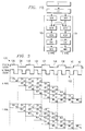
- Figure 3 illustrates the flow of four instructions per pipeline, showing the overlapping execution of the instructions, for a two pipeline architecture. Additional pipelines and additional stages for each pipeline could also be provided.
- the microprocessor 10 uses an internal clock 122 which is a multiple of the system clock 124.
- the internal clock is shown as operating at two times the frequency of the system clock.
- the ID1 stage operates on respective instructions X0 and Y0.
- instructions X0 and Y0 are in the ID2 stage (X0 being in ID2x and Y0 being in ID2y) and instructions X1 and Y1 are in the ID1 stage.
- instructions X2 and Y2 are in the ID1 stage
- instructions X1 and Y1 are in the ID2 stage (X1 being in ID2x and Y1 being in ID2y) and instructions X0 and Y0 are in the AC1 stage (X0 being in AC1x and Y0 being in AC1y).
- instructions X3 and Y3 are in the ID1 stage
- instructions X2 and Y2 are in the ID2 stage
- instructions X1 and Y1 are in the AC1 stage
- instructions X0 and Y0 are in the AC2 stage.
- the instructions continue to flow sequentially through the stages of the X and Y pipelines.
- clocks 134-140 the execution portion of each instruction is performed on sequential clock cycles. This is a major advantage of a pipelined architecture - the number of instructions completed per clock is increased, without reducing the execution time of an individual instruction. Consequently a greater instruction throughput is achieved with greater demands on the speed of the hardware.
- each pipe stage completes on time and no stage requires more than one clock cycle. In an actual machine, however, one or more stages may require additional clock cycles to complete thereby changing the flow of instructions through the other pipe stages. Furthermore, the flow of instructions through one pipeline may be dependent upon the flow of instructions through the other pipeline.
- a number of factors may cause delays in various stages of one or all of the pipelines. For example, an access to memory may miss in the memory cache, thereby preventing access of the data in the time required to process the instruction in one clock. This would require that either, or both, sides of the AC1 stage to delay until the data was retrieved from main memory. For a particular stage, other stages of the pipeline may be using a needed resource, such as a multiplier, which is only in one of the execution stages in the illustrated embodiment. In this case, the stage must delay until the resource is available. Data dependencies can also cause delays. If an instruction needs the result from a previous instruction, such as an ADD, it must wait until that instruction is processed by the execution unit.
- a needed resource such as a multiplier
- multi-box instructions i.e., instructions which are implemented using multiple microinstructions, and therefore require more than one clock cycle to complete. These instructions stop the flow of subsequent instructions through the pipeline at the output of the ID2 stage.
- the flow of instructions through the pipeline is controlled by the pipe control unit 28.
- a single pipe control unit 28 is used to control the flow of instructions through both (or all) of the pipes.
- the pipe control unit 28 receives "delay" signals from the various units comprising the pipelines 102 and 104, and issues "stall" signals to the various units.
- a single pipe control unit 28 is used for both X and Y pipelines, the pipelines themselves are controlled independent of one another. In other words, a stall in the X pipeline does not necessarily cause a stall in the Y pipeline.
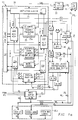
- Figure 4a depicts a block diagram having certain components involved in the generation of microaddresses and the resulting microinstructions. While the blocks of Figure 4a derive from those in Figure 1, it should be understood that the method of the present invention is not necessarily limited by the particular locations of specific components, and one skilled in the art may relocate various functionality without departing from the inventive scope.
- instructions for both the x- and y-pipelines are coupled to an instruction decoder 21. Decoder 21 receives the x- and y-instructions and provides both microaddresses and control to microcontrol unit 26. More particularly, the microaddresses and control are coupled to a microsequencer circuit 146 within microcontrol unit 26.
- microsequencer circuit 146 includes independent microsequencers 146x and 146y for performing like functions with respect to the x- and y-pipelines. Microsequencer circuit 146 also receives both control and microaddresses from other sources (not shown) throughout the microprocessor. Microsequencer circuit 146 is coupled to provide addresses, hereinafter referred to as microaddresses, to address the memory (shown and described later) in a microROM circuit 148.
- Figure 4b illustrates the timing of microaddress generation, microinstruction generation, and microinstruction execution by the blocks of Figure 4a. Note that the timing of Figure 4b derives from Figure 3, but with greater emphasis on the stages corresponding to the operations of the blocks of Figure 4a. Note also that the stages of Figure 4b illustrate the sequence of an x- and y-instruction through four internal clock cycles evenly numbered 150 through 156. Clock cycles 150 through 156 include the ID2, AC1, AC2 and EX stages. Note also that each clock cycle includes two phases, denoted ⁇ 1 and ⁇ 2.
- instruction decoder 21 determines the number of bytes in the single clock instruction and the types of fields included in the instruction. Decoder 21 also provides entry point microaddresses derived from the instructions for addressing microROM circuit 148.
- microsequencer circuit 146 outputs the next microaddress for microROM circuit 148 for both the x- and y-instruction.
- the next microaddresses are labeled as ⁇ sx 1 and ⁇ sy 1 , respectively, with ⁇ s indicating output from the microsequencer.
- ⁇ sx 1 is output by microsequencer circuit 146 during the first phase, ⁇ 1, of stage ID2.
- ⁇ sy 1 is output by microsequencer circuit 146 during the second phase, ⁇ 2, of stage ID2.
- Microsequencer circuit 146 operates as a sophisticated multiplexer; thus, in response to its control signals, microsequencer circuit 146 chooses from its microaddress inputs to output the next microaddress.
- the next microaddress selected and output by microsequencer circuit 146 may be one of eight different microaddresses. The provision of some of the microaddresses is specifically described throughout this document, with it understood that the remainder fall within the general indication in Figure 4a of an input providing microaddresses to multiplexer circuit 146. Briefly, the seven different microaddresses are:
- microaddresses are applied by microsequencer circuit 146 to microROM circuit 148, which outputs a microinstruction to carry out whatever functionality is called for by the corresponding microaddress.
- ⁇ sx 1 is applied to microROM circuit 148.
- an array within microROM circuit 148 generates and outputs the corresponding microinstruction, labeled ⁇ rx 1 .
- ⁇ r suggests output from microROM circuit 148.
- microROM circuit 148 immediately following the output of microaddress ⁇ sy 1 (following ⁇ 2 of stage ID2), ⁇ sy 1 is applied to microROM circuit 148. Also as detailed in section 4, below, between ⁇ 1 and by the end of ⁇ 2 of stage AC1, the array of microROM circuit 148 generates and outputs the corresponding microinstruction, labeled ⁇ ry 1 . Stage AC2 occurs in clock cycle 154 and the microinstructions corresponding to instructions X1 and Y1, ⁇ rx 1 and ⁇ ry 1 , are presented to the applicable components of the microprocessor. Note in the preferred embodiment that each pipeline has its own respective address calculation stage and, thus, the x- and y-microinstructions are presented accordingly.
- clock cycle 154 is illustrated as applying to both "x 1 & y 1 " during the entire duration of the AC2 stage.
- each respective microinstruction is decoded in preparation for execution.
- stage EX occurs in clock cycle 156, where the decoded instructions are applied to respective x- and y-pipeline ALUs, thereby executing the functions specified by the presented microinstructions.
- the x- and y-operations occur independently of one another and, hence, are illustrated as applying to both "x 1 & y 1 " during the entire duration of the EX stage. Note that because Figure 4b corresponds to the flow of a single clock instruction, only a single clock cycle 156 is necessary for the execution stage of the instruction. Multiple clock instructions require additional execution stages.
- one aspect of the present invention pertains to enhancing the timing of output by microROM circuit 148 immediately following a single clock instruction.
- the present invention recognizes that once a given instruction is determined to be a single clock instruction, it is desirable to advance the next successive instruction through the pipeline as soon as possible. More specifically, when the instruction presently passing through a pipeline is a single clock instruction and, thus, requires only a single clock cycle for its EX stage, it is preferable to immediately advance the next successive instruction so that it follows only one stage behind the present single clock instruction.
- Figure 4c illustrates this preferred scenario.
- Figure 4c illustrates a timing diagram including the instruction flow for two successive instructions through the x- and y-pipelines over the same clock cycles 150 through 156 shown in Figure 4b.
- Subscripts in Figure 4c illustrate the succession of the two instructions.
- the first x- and y-instructions denoted with a subscript one, are single clock instructions and flow in the same manner as the instruction shown in Figure 4b.
- the second x- and y-instructions denoted with a subscript two, are additional instructions which follow one stage immediately behind the first x- and y-instructions. Given the immediate succession of instruction flow, no stage is wasted, that is, no clock cycle occurs during the illustrated instruction flow where the instruction is not processed by either the ID1, ID2, AC1, AC2, or EX stage.
- Figure 4d illustrates a timing diagram of the flow in the prior art for the two paired instructions of Figure 4c. Note that the microsequencer outputs for the second instruction, ⁇ sx 2 and ⁇ sy 2 , are output during clock cycle 154, rather than clock cycle 152 as shown in the inventive preferred flow of Figure 4c. Thus, clock cycle 152 is wasted in the prior art. Such a result occurs because of the prior art methodology in controlling the microsequencer circuit's output.
- the microinstruction output by the microROM for a single clock instruction, ⁇ r includes a control signal which subsequently (after a wasted clock cycle) causes the microsequencer circuit to output the next microROM microaddress, ⁇ s. More particularly, for each different microinstruction, a given bit or bits in ⁇ r indicate that an instruction is a single clock instruction. Only after this indication is the microsequencer caused to output the next microaddress, ⁇ s. This indication and delay is shown by an arrow in Figure 4d. As shown, at the end of ⁇ 1 of clock cycle 152, the microinstruction, ⁇ rx1, indicates that its corresponding instruction is a single clock instruction.
- next microaddress, ⁇ sx2 is output only after this indication and, thus, cannot occur until the beginning of clock cycle 154.
- the microsequencer must "wait on” the microROM output and, hence, at least one clock cycle is wasted during this waiting period. Note that the same delay occurs for the y-pipeline as shown by the delay arrow in Figure 4d between the microROM output ⁇ ry1, and the responsive next output by the microsequencer, ⁇ sy2.
- the present invention includes a novel apparatus and methodology for achieving the preferred and improved flow of Figure 4c, and is described below.
- Figure 5 illustrates the block diagram of Figure 4a, but with additional details used to achieve the preferred timing of Figure 4c.
- instruction decoder 21 includes separate registers 21x and 21y for the x- and y-instructions, respectively.
- each separate register 21x and 21y is coupled to a respective programmable logic array (PLA).
- PLAs 158x and 158y are coupled to the portions of registers 21x and 21y storing the opcode of each instruction. Note that while the opcode is illustrated as left-justified within each respective register 143x and 143y, such an illustration is arbitrary in that the opcode may be stored anywhere within the buffer and is not necessarily represented by contiguous bits therein.
- Each PLA 158x and 158y is further coupled to the control input of a respective microsequencer 146x and 146y. Lastly, while not illustrated, note that each PLA 158x and 158y may be further coupled to additional inputs to perform the functionality described below.
- each instruction register 21x and 21y stores two sequentially pipelined instructions, x 1 and x 2 , and y 1 and y 2 , respectively.
- microsequencer 146x receives control signals and outputs the next microaddress, ⁇ sx 1 .
- microsequencer 146y receives control signals and outputs the next microaddress, ⁇ sy 1 .
- ⁇ sx 1 and ⁇ sy 1 are output, they are applied to microROM circuit 148 to generate ⁇ rx 1 and ⁇ ry 1 as described above.
- each PLA 158x and 158y decodes the opcode of the respective instruction to determine whether the current instruction is a single clock instruction.
- the PLA is programmed to detect any possible pattern of opcode bits which comprise a single clock instruction. This detection may be based on a portion or all of the opcode bits. If the PLA detects a single clock instruction, the PLA controls its respective microsequencer to output the next microaddress, ⁇ s, during the immediately following clock cycle.
- PLA 158x determines that instruction x 1 is a single clock instruction
- PLA 158x controls microsequencer 146x to output the next microaddress, ⁇ sx 2 , during the next clock cycle 152 as shown in Figure 4c.
- PLA 158y determines that instruction y 1 is a single clock instruction
- PLA 158y controls microsequencer 146y to output the next microaddress, ⁇ sy 2 , during the next clock cycle 152 as shown in Figure 4c.
- each PLA 158x and 158y may analyze information in addition to selected opcode bits determine whether an instruction is a single clock instruction. For example, in an X86 architecture, other bits within the instruction may be analyzed, such as selected bits of the mod r/m byte. Moreover, in addition to opcode bits, bits outside the instruction may also be analyzed. For example, a bit indicating whether or not the protected mode is set also may be analyzed in determining whether an instruction is a single clock instructions. Other examples may become known to a person skilled in the art, and are intended as within the scope of the present invention.
- the present invention also applies to a dual pipeline architecture when only one of the two pipelines is executing a single clock instruction (i.e., irrespective of the number of execution stages required by the instruction in the other pipeline).
- the invention also applies to other single or multiple pipeline architectures.
- a PLA is shown monitoring opcode bits
- structure other than a PLA may be used to detect the presence of a single clock instruction.
- bits other than opcode bits may, given a particular architecture, be analyzed if representative of a single clock instruction.
- the processor architecture of the present invention includes a microROM circuit 148 which receives microaddresses, and produces microinstructions, in accordance with the timing diagram of Figure 4c.
- the present invention uses additional novel apparatus and methodology to achieve such timing while using a single microROM array. Particularly, Figure 6 illustrates such apparatus, and Figure 7 illustrates the detailed timing for the apparatus of Figure 6.
- microROM circuit 148 is shown in greater detail using blocks to represent various functionality.
- the blocks include a single microROM array 167 which services both the x- and y-pipelines.
- MicroROM array 167 includes a plurality of rows and columns for storing microinstructions which are addressed and output by the various blocks of Figure 6. With the exception of two components described below, the remainder are generally symmetric about microROM array 167; accordingly, the following description focuses on the x-related blocks, with corresponding reference numerals using the "x" designation. Components pertaining to the y-related blocks are likewise labeled, but use the "y" designation.
- the microaddress, ⁇ sx is coupled to the input of a latch 152x which is clocked by ⁇ 1.
- ⁇ sx is a fourteen bit address which is broken into separate components for addressing a row and column of microROM array 167, respectively.
- microinstructions are stored in array 167 such that sixteen instructions are stored along a row.
- ten bits of ⁇ sx are coupled from latch 152 to the input of a row decode block 154x.
- four bits of ⁇ sx are coupled from latch 152 to the input of a column decode block 156x.
- ⁇ sx While the groups of ten bits are shown as the first ten bits of ⁇ sx (i.e., [0:9]) and the last four bits of ⁇ sx (i.e., [10:13]), it should be understood that non-contiguous bits of ⁇ sx may be selected for either row or column decoding. It also should be understood that the microaddresses, ⁇ sx and ⁇ sy, may consist of more or less than fourteen bits.
- the output of row decode block 154x is coupled to the input of a latch 158x clocked by ⁇ 2. Further, the output of latch 158x is coupled to the input of a tristate driver 160x clocked by ⁇ 1. Similarly, the output of column decode block 156x is coupled to the input of a latch 162x, which is clocked by ⁇ 2.
- tristate driver 160x is coupled to an address bus denoted 164xy suggesting, as discussed below, that either x- or y-addresses may be communicated on the bus. Indeed, note that the output of tristate driver 160y is also coupled to address bus 164xy. Address bus 164xy is coupled to the input of row driver 166xy, which is further coupled to microROM array 167.
- the circuitry symmetry in Figure 6 creates componentry for the y-row related circuitry similar to that just described in connection with x-row related circuitry. Thus, bits [0:9] of ⁇ sy are coupled to a row decode block 154y which has an output coupled to the input of a latch 158y.
- latch 158y is coupled to the input of a tristate driver 160y, which has an output coupled to address bus 164xy. Note, however, that although the data path for the y-row circuitry is similar to the x-row circuitry, the clock signals for latch 158y and driver 160y are switched to achieve the timing function described below.
- the output of latch 162x is coupled to the control inputs of a sense amplifier, latch and multiplexer block 168x.
- block 168x is capable of performing each of the functions of its name.
- the data input of block 168x is coupled to an output of microROM array 167.
- block 168x is clocked by ⁇ 1 to performing a latching function.
- block 168x latches only selective portions (i.e., a particular column) of a row of data output by microROM array 167 as discussed in greater detail below.
- the output of block 168x is coupled to the input of a flip flop 170x which is clocked by ⁇ 1.
- the output of flip flop 170x is coupled to any line, bus, or architecture which requires access to the x-microinstruction produced by microROM array 167.
- circuitry symmetry in Figure 6 creates similar componentry for the y-column related circuitry.
- bits [10:13] of ⁇ sy are coupled to a column decode block 156y which is further coupled to the input of a latch 162y.
- the output of latch 162y is coupled to the control input of a sense amp, latch and multiplexer block 168y.
- the y-column data path is therefore generally the same as they x-row data path, but the clocking signals are reversed to achieve the timing described below. Note also, however, that the y-row data path differs slightly in one regard, namely, the output of multiplexer block 168y is coupled to the input of a latch 172y.
- multiplexer block 168x which is coupled to a flip flop rather than a latch. This difference also accommodates the timing functionality described below.
- the output of latch 172y is coupled to any line, bus, or architecture which requires access to the y-microinstruction produced by microROM array 167.
- one invention of the preferred architecture involves two accesses of microROM circuit 148 in the same clock cycle 150, but in separate phases, ⁇ 1 and ⁇ 2. Further, by applying ⁇ rx and ⁇ ry to microROM circuit 148 in a single clock cycle, ⁇ rx is fully available by the end of one clock cycle after ⁇ sx and, similarly, ⁇ ry is fully available by the end of one clock cycle after ⁇ sy.
- the blocks of Figure 6 permit such operation, and are best understood by the more detailed timing diagram of Figure 7.
- Figure 7 illustrates a detailed timing diagram for both the x- and y-accessing of microROM array 167 during the clock cycles 150 through 154, similar to that shown in Figure 4b.
- the operation in connection with the x-pipeline i.e., x-microaddress and x-microinstruction
- the y-pipeline i.e., y-microaddress and y-microinstruction
- ⁇ sx 1 is latched by latch 152x by the close of ⁇ 1 of clock cycle 150. Accordingly, the appropriate bits of ⁇ sx 1 are provided to row and column decode blocks 154x and 156x, respectively. Each of these decode blocks decodes the bits according to principles known in the art to identify the corresponding row and column within microROM array 167 which are addressed by ⁇ sx 1 . Thus, the microaddress decode occurs during ⁇ 2 of clock cycle 150, and resulting row and column decoded signals are latched at the close of ⁇ 2 of clock cycle 150 by latches 158x and 162x, respectively. Note the decoded column signal output by latch 162x is immediately coupled to the control input of multiplexer block 168x.
- tristate driver 160x drives address bus 164xy with the decoded row value latched in latch 158x. This value is received by driver 166xy which, in accordance with principles known in the art, provides a sufficient driving signal(s) to the selected row of microROM array 167.
- driver 166xy which, in accordance with principles known in the art, provides a sufficient driving signal(s) to the selected row of microROM array 167.
- the driving operation and response by microROM array 167 generates and operates the appropriate signals of the addressed row.
- multiplexer 168x latches selected bits of the row of signals output by microROM array 167.
- certain bits are selected in response to the decoded column address received from latch 162x and latched to the output of multiplexer 168x. Note that this event also corresponds to the end of ⁇ 1 during clock cycle 152 shown in Figure 4b, above.
- flip flop 170x samples its input and, upon the falling edge of ⁇ 2, flip flop 170x outputs the sampled input. Accordingly, at the end of ⁇ 2 of cycle 152, the x-pipeline microinstruction, ⁇ rx, is available to the remainder of the processor for operation of the AC2 stage described above. Note also that flip flop 170x is included to isolate the current microinstruction from any potential changes occurring in the output of microROM array 167 or multiplexer 168x.
- any change in the output of either microROM array 167 or multiplexer 168x does not affect the output of flip flop 170x during the next phase, ⁇ 1 of cycle 154.
- any such change will not affect the components of the processor examining the current ⁇ rx microinstruction.
- ⁇ sy 1 is latched by latch 152y by the close of ⁇ 2 of clock cycle 150. Accordingly, the appropriate bits of ⁇ sy 1 are provided to row and column decode blocks 154y and 156y, respectively. Like the x-bits, but one phase later, the y-bits are decoded during ⁇ 2 of clock cycle 150 to identify the corresponding row and columns within microROM array 167 which are addressed by ⁇ sy 1 . Moreover, the resulting row and column decoded signals are latched at the close of ⁇ 1 of clock cycle 152 by latches 158y and 162y, respectively.
- tristate driver 160y drives address bus 164xy with the decoded row value latched in latch 158y.
- tristate driver 160x is in a high impedance mode during this time so that only the y-address is communicated to the address bus 164xy. Again, this value is received by driver 166xy which drives the selected row of microROM array 167.
- the driving operation and response by microROM array 167 generates and outputs the appropriate signals of the addressed row.
- multiplexer 168y latches selected bits (i.e., a column) of the row of signals output by microROM array 167. In this instance, these bits, which represent the desired microinstruction, are selected in response to the decoded column address received from latch 162y and latched to the output of multiplexer 168y. Note that this event also corresponds to the end of ⁇ 2 during clock cycle 152 shown in Figure 4b, above.
- latch 172y becomes transparent so that the signals at its inputs become available at its outputs.
- the remainder of the processor has access to the y-pipeline microinstruction, ⁇ ry.
- latch 172y like that flip flop 170x, is included to isolate the current microinstruction from any potential changes occurring in the output of microROM array 167 or multiplexer 168y.
- any change in the output of either microROM array 167 or multiplexer 168y does not affect the output of latch 172y during the next phase, ⁇ 2 of cycle 154.
- any such change will not affect the components of the processor examining the current ⁇ ry microinstruction.
- the preferred embodiment includes a microsequencer circuit 146 which operates as a sophisticated multiplexer to choose between various microaddresses at its inputs and output the selected microaddress for addressing microROM circuit 148.
- the present invention further includes apparatus and methodology for expediting the execution of condition dependent instructions.
- a condition dependent instruction is a change of flow (“COF") instructions.
- COF instructions are known in the art and, include, by way of example in the X86 architecture, instructions such as FAR JUMP, FAR CALL, and IRET.
- the preferred apparatus and methodology for expediting such COF instructions, as well as other condition dependent instructions, are described in connection with Figure 8, immediately below.
- Figure 8 illustrates a portion of the components of Figure 4a, with additional apparatus for expediting condition dependent instructions.
- the preferred embodiment is discussed, by way of example, as applying to COF instructions.
- the COF instruction is by way of example, and is not intended to limit the scope of the invention as defined by its claims. Therefore, continuing with Figure 8, it again illustrates microsequencer circuit 146 receiving microaddresses and, via various control signals, providing microaddresses ⁇ sx and ⁇ sy to microROM circuit 148.
- apparatus in addition to Figure 4a is shown for providing microaddresses and control in connection with COF instructions.
- Figure 8 further illustrates a COF instruction decode circuit 174.
- COF instruction decode circuit 174 includes various data inputs, preferably including an input 176a for receiving descriptors, an input 176b for receiving mode bits, and an input 176c for receiving "history bits.” History bits include selected bits stored from previously issued instructions and/or bits from previously executed microinstructions corresponding to the present instruction being executed. COF instruction decode circuit further includes control inputs 178x and 178y for receiving control signals corresponding to the respective x- and y-instructions. For purposes more readily apparent below, these control signals are referred to herein as the x-Multiway and y-Multiway control signals, respectively.
- COF instruction decode circuit further includes an output 180xy, which is illustrated as splitting into respective x- and y-outputs 180x and 180y.
- Output 180x is coupled to provide a SECONDARY ADDRESS to the lower portion of an address register 182x, or a DONE signal to control microsequencer 146x.
- output 180y is coupled to provide the SECONDARY ADDRESS to the lower portion of an address register 182y, or the DONE signal to control microsequencer 146y.
- the upper portion of address register 182x is coupled to the x-output of microROM circuit 148 and, thus, is capable of receiving a portion of the x-microinstruction, ⁇ rx.
- this connection permits ⁇ rx to provide a BASE ADDRESS to the upper portion of address register 182x, Similarly, the upper portion of address register 182y is coupled to the y-output of microROM circuit 148 and, thus, is capable of receiving a portion of the y-microinstruction, ⁇ ry. Thus, also as described in greater detail below, this connection permits ⁇ ry to provide a BASE ADDRESS to the upper portion of address register 182y.
- condition #1 the microROM would output address 10, which is the next (or "destination") microinstruction address within itself for continuing the execution of the COF instruction.
- the process flow would then sequence by jumping to the microinstruction at location 10, and continue until the functionality for the COF instruction was completed.
- condition #1 were not met, however, then a counter was used to increment a portion of the microaddress which identified the then-executing microinstruction.
- the incremented value would identify address 2 and so the sequence would address the microinstruction at that address.
- the successive microinstruction would test another condition, namely, condition #2. The process would repeat until a condition was met, or all conditions in the succession were tested with no satisfaction.
- microROM would issue a DONE signal, thereby indicating that the COF instruction had completed its execution cycle, and the instruction entry point into the microROM for the next instruction could be accessed. Note that the above example uses sequential numbers only to facilitate an understanding of the concept, but is not intended to indicate that the conditional microinstructions are necessarily addressed in an integer incremental fashion.
- the COF (or other condition dependent) instruction is received by the instruction decoder (see, e.g., Figure 4a)
- its execution stage commences by issuing a control signal from microROM circuit 148.
- this signal is identified herein as "Multiway,” indicating that flow can be directed to multiple, differing destinations (i.e., ways) in the next successive clock cycle.
- an x-Multiway control signal is output by microROM circuit 148 as part of the x-microinstruction.
- the x-Multiway control signal controls COF instruction decode circuit 174 as described below.
- the x-microinstruction also simultaneously includes a BASE ADDRESS which loads into the upper portion of address register 182x.
- COF instruction decode circuit 174 preferably includes combinatorial logic which analyzes the preferred information at its inputs 176a, 176b, and 176c, and determines a SECONDARY ADDRESS in response to those inputs.
- the SECONDARY ADDRESS is preferably calculated based on the input information before the issuance of the Multiway control signal. Thereafter, as in the example of the x-Multiway control signal above, issuance of the Multiway control signal causes the already-determined SECONDARY ADDRESS to load from COF instruction decode circuit 174 into the lower portion of address register 182x.
- both the lower and upper portions of address register 182x are loaded with address portions. Those portions are then combined, preferably by concatenation, to form a single DESTINATION ADDRESS.
- This DESTINATION ADDRESS is the location within microROM circuit 148 for proceeding with the execution of the COF instruction. Accordingly, the DESTINATION ADDRESS is coupled to microsequencer 146x which selects it and couples it to microROM circuit 148, thereby addressing and executing the next microinstruction of the execution stage for the COF instruction.
- decode circuit 174 outputs it SECONDARY ADDRESS to the lower portion of address register 182x
- the same SECONDARY ADDRESS is output to the lower portion of address register 182y.
- a different BASE ADDRESS is provided from microROM circuit 148, and this different BASE ADDRESS combines with the SECONDARY ADDRESS in the same manner, and for the same purpose, as described in connection with the x-pipeline.
- the DONE signal is also coupled simultaneously from decode circuit 174 to both microsequencer 146x and 146y.
- COF instruction decode circuit 174 may provide a DONE signal to control microsequencer 146x in lieu of providing the SECONDARY ADDRESS to address register 182x as detailed above. This same functionality applies to the y-components and, hence, COF instruction decode circuit 174 may provide a DONE signal to control microsequencer 146y in lieu of providing the SECONDARY ADDRESS to address register 182y. This feature also provides advantages over the prior art.
- COF instruction decode circuit 174 operates independently of accesses to microROM circuit 148. Moreover, in the present embodiment, because of the various input data available to COF instruction decode circuit 174, it determines when a COF instruction has completed its execution stages. Thus, when the Multiway control signal is received by COF instruction decode circuit 174, in lieu of a SECONDARY ADDRESS, it outputs a DONE signal if the combination of its inputs indicates completion of the execution of the COF instruction. In the preferred embodiment, the DONE signal is encoded in the same four bit output from decode circuit 174 discussed above in connection with the SECONDARY ADDRESS. Such a configuration permits dual use of the same conductors without an independent output. One skilled in the art, however, may readily appreciate that a separate output could be provided, with more or less bits, for communicating the DONE signal.
- the DONE signal from COF instruction decode circuit 174 is coupled to microsequencer circuit 146 and controls the microsequencer circuit 146 such that the next microaddress it selects is the entry point microaddress to the instruction following the COF instruction. Accordingly, one skilled in the art may appreciate that the present invention immediately indicates the completion of the COF instruction without requiring the microROM to indicate such status. Thus, one or more clock cycles are saved over the known prior art embodiment described above.
Landscapes
- Engineering & Computer Science (AREA)
- Software Systems (AREA)
- Theoretical Computer Science (AREA)
- Physics & Mathematics (AREA)
- General Engineering & Computer Science (AREA)
- General Physics & Mathematics (AREA)
- Advance Control (AREA)
- Executing Machine-Instructions (AREA)
Claims (14)
- Processeur comprenant :un décodeur (21x) pour mémoriser des instructions devant être décodées ;une mémoire (148) réagissant à une micro-adresse en délivrant en sortie une micro-instruction associée à une instruction mémorisée dans ledit décodeur (21) ; etdes circuits de séquenceur (146x) couplés de façon à délivrer une micro-adresse à ladite mémoire (148) ;
caractérisé par un détecteur (158x) couplé au décodeur (21x) et pouvant fonctionner de façon à détecter si oui ou non une instruction comprend une instruction d'horloge unique avant que ladite mémoire (148) ne délivre en sortie la micro-instruction associée à cette instruction, ledit détecteur (158x) réagissant à la détection d'une instruction d'horloge unique en entrant un signal de commande sur les circuits de séquenceur (146x) de façon à faire délivrer par les circuits de séquenceur, indépendamment de ladite mémoire (148), une autre micro-adresse associée à une autre instruction. - Processeur selon la revendication 1, comprenant :des deuxièmes circuits de séquenceur (146y) couplés de façon à délivrer une micro-adresse afin de faire délivrer en sortie par ladite mémoire (148) une micro-instruction associée à une autre instruction mémorisée par ledit décodeur (21) ; etun deuxième décodeur (21y) couplé de façon à recevoir des instructions dudit décodeur (21x), un deuxième décodeur (158y) pour détecter si oui ou non ladite autre instruction comprend une instruction d'horloge unique avant que ladite mémoire (148) ne délivre en sortie la micro-instruction associée à cette autre instruction, ledit deuxième décodeur (158y) réagissant à la détection d'une instruction d'horloge unique en entrant un signal de commande sur les deuxièmes circuits de séquenceur (146y) de façon à faire délivrer par les deuxièmes circuits de séquenceur, indépendamment de ladite mémoire (148), une autre micro-adresse associée à une autre instruction.
- Processeur selon la revendication 2, dans lequel lesdits décodeurs (21x, 21y) comprennent des registres respectifs.
- Processeur selon l'une quelconque des revendications 1 à 3, dans lequel ledit détecteur ou chacun desdits détecteurs (158x, 158y) réagit à la détection d'une instruction d'horloge unique en entrant un signal de commande sur ses circuits de séquenceur associés (146x, 146y), de façon à faire délivrer à ces circuits de séquenceur ladite autre micro-adresse dans le cycle d'horloge suivant.
- Processeur selon l'une quelconque des revendications 1 à 4, dans lequel ledit ou chacun desdits détecteurs (158x, 158y) comprend un groupement logique programmable.
- Processeur selon la revendication 5, dans lequel ledit ou chacun desdits groupements logiques programmables détecte des bits sélectionnés d'une instruction pour détecter si oui ou non ladite instruction est une détermination d'instruction d'horloge unique.
- Processeur selon l'une quelconque des revendications précédentes, dans lequel ledit détecteur ou chacun desdits détecteurs (158x, 158y) réagit à une pluralité de bits de code opération d'instructions mémorisés dans ladite mémoire (148) en détectant si oui ou non une instruction est une instruction d'horloge unique.
- Processeur selon la revendication 7, dans lequel ledit ou chacun desdits détecteurs (158x, 158y) réagit également à un bit de mode protégé extérieur à une instruction en détectant si oui ou non une instruction est une instruction d'horloge unique.
- Processeur selon l'une quelconque des revendications précédentes, dans lequel la mémoire (148) est une micro-mémoire morte.
- Procédé de fonctionnement d'un processeur, le procédé comprenant les étapes suivantes :la mémorisation d'instructions ;la délivrance en sortie d'une micro-adresse à partir d'un séquenceur (146x) pour adresser une mémoire (148), de façon à faire par conséquent délivrer par la mémoire (148) une micro-instruction associée à une instruction mémorisée ;
caractérisé par la détection, avant que ladite mémoire (148) ne délivre en sortie la micro-instruction associée à une instruction, du fait que oui ou non cette instruction est une instruction d'horloge unique ; et, en réponse à la détection d'une instruction d'horloge unique, par l'entrée d'un signal de commande sur le séquenceur (146x), pour délivrer, indépendamment de ladite mémoire (148), une autre micro-adresse associée à une autre instruction. - Procédé selon la revendication 10, caractérisé de plus par la mémorisation d'autres instructions ; et, sensiblement en parallèle avec la mise en oeuvre du procédé selon la revendication 10, par la délivrance en sortie d'une micro-adresse à partir d'un autre séquenceur (146y), de façon à adresser ladite mémoire (148), de façon à faire par conséquent délivrer par la mémoire une micro-instruction associée à une autre instruction mémorisée ; par la détection, avant que ladite mémoire (148) ne délivre en sortie la micro-instruction associée à ladite autre instruction, du fait que oui ou non cette autre instruction est une instruction d'horloge unique ; et, en réponse à la détection d'une autre instruction d'horloge unique, par l'entrée d'un signal de commande sur l'autre séquenceur (146y), pour délivrer, indépendamment de ladite mémoire (148), une autre micro-adresse associée à une autre instruction.
- Procédé selon la revendication 10 ou 11, dans lequel ladite détection est effectuée par le décodage logique d'une partie présélectionnée d'une instruction afin de détecter si oui ou non ladite instruction est une instruction d'horloge unique.
- Procédé selon l'une quelconque des revendications 10 à 12, dans lequel, en réponse à la détection d'une instruction d'horloge unique, le signal de commande entré sur l'un des séquenceurs (146x) et l'autre séquenceur (146y) provoque la délivrance d'une autre micro-adresse associée à une autre instruction dans le cycle d'horloge suivant.
- Procédé selon l'une quelconque des revendications 10 à 13, caractérisé de plus par la répétition dudit procédé pour une série d'instructions.
Applications Claiming Priority (6)
| Application Number | Priority Date | Filing Date | Title |
|---|---|---|---|
| US13832093A | 1993-10-18 | 1993-10-18 | |
| US08/138,660 US5794026A (en) | 1993-10-18 | 1993-10-18 | Microprocessor having expedited execution of condition dependent instructions |
| US08/138,855 US5644741A (en) | 1993-10-18 | 1993-10-18 | Processor with single clock decode architecture employing single microROM |
| US138320 | 1993-10-18 | ||
| US138660 | 1993-10-18 | ||
| US138855 | 1993-10-18 |
Publications (3)
| Publication Number | Publication Date |
|---|---|
| EP0649083A2 EP0649083A2 (fr) | 1995-04-19 |
| EP0649083A3 EP0649083A3 (fr) | 1995-05-10 |
| EP0649083B1 true EP0649083B1 (fr) | 2000-07-19 |
Family
ID=27385166
Family Applications (1)
| Application Number | Title | Priority Date | Filing Date |
|---|---|---|---|
| EP94307581A Expired - Lifetime EP0649083B1 (fr) | 1993-10-18 | 1994-10-17 | Microcontrôleur pour microprocesseur superpipeline et superscalaire |
Country Status (4)
| Country | Link |
|---|---|
| US (1) | US5771365A (fr) |
| EP (1) | EP0649083B1 (fr) |
| JP (1) | JP3736866B2 (fr) |
| DE (1) | DE69425310T2 (fr) |
Families Citing this family (12)
| Publication number | Priority date | Publication date | Assignee | Title |
|---|---|---|---|---|
| EP0649085B1 (fr) | 1993-10-18 | 1998-03-04 | Cyrix Corporation | ContrÔle de pipeline et traduction de régistre pour microprocesseur |
| KR100384875B1 (ko) * | 1995-12-16 | 2003-08-21 | 주식회사 하이닉스반도체 | 파이프라인구조를갖는마이크로프로세서에서의언세이프처리마이크로시퀀서 |
| WO2000004484A2 (fr) * | 1998-07-17 | 2000-01-27 | Intergraph Corporation | Processeur graphique a mot instruction long |
| US6957322B1 (en) * | 2002-07-25 | 2005-10-18 | Advanced Micro Devices, Inc. | Efficient microcode entry access from sequentially addressed portion via non-sequentially addressed portion |
| US6851033B2 (en) * | 2002-10-01 | 2005-02-01 | Arm Limited | Memory access prediction in a data processing apparatus |
| US9454490B2 (en) | 2003-05-12 | 2016-09-27 | International Business Machines Corporation | Invalidating a range of two or more translation table entries and instruction therefore |
| US7530067B2 (en) * | 2003-05-12 | 2009-05-05 | International Business Machines Corporation | Filtering processor requests based on identifiers |
| US7284100B2 (en) * | 2003-05-12 | 2007-10-16 | International Business Machines Corporation | Invalidating storage, clearing buffer entries, and an instruction therefor |
| CA2545252A1 (fr) * | 2003-11-06 | 2005-05-26 | University Of Nevada, Reno | Procedes ameliores pour la detection et la mesure de sequences d'acides nucleiques specifiques |
| US7743233B2 (en) * | 2005-04-05 | 2010-06-22 | Intel Corporation | Sequencer address management |
| US9182984B2 (en) | 2012-06-15 | 2015-11-10 | International Business Machines Corporation | Local clearing control |
| CN115080116B (zh) * | 2022-07-25 | 2022-11-29 | 广州智慧城市发展研究院 | 兼容多种存储器接口的微控制器、方法、芯片和显示器 |
Family Cites Families (12)
| Publication number | Priority date | Publication date | Assignee | Title |
|---|---|---|---|---|
| GB2112973B (en) * | 1978-11-08 | 1983-12-21 | Data General Corp | High-speed digital computer system |
| US4430706A (en) * | 1980-10-27 | 1984-02-07 | Burroughs Corporation | Branch prediction apparatus and method for a data processing system |
| US4984151A (en) * | 1985-03-01 | 1991-01-08 | Advanced Micro Devices, Inc. | Flexible, next-address generation microprogram sequencer |
| US4685088A (en) * | 1985-04-15 | 1987-08-04 | International Business Machines Corporation | High performance memory system utilizing pipelining techniques |
| DE3650473T2 (de) * | 1985-11-08 | 1996-08-14 | Nippon Electric Co | Mikroprogrammsteuereinheit |
| JPH0743648B2 (ja) * | 1985-11-15 | 1995-05-15 | 株式会社日立製作所 | 情報処理装置 |
| EP0279953B1 (fr) * | 1987-02-24 | 1994-11-02 | Texas Instruments Incorporated | Ordinateur exécutant un mélange de micro- et macro-instructions |
| US5032983A (en) * | 1987-04-10 | 1991-07-16 | Tandem Computers Incorporated | Entry point mapping and skipping method and apparatus |
| JPH01271838A (ja) * | 1988-04-22 | 1989-10-30 | Fujitsu Ltd | マイクロプログラム分岐方法 |
| US5088035A (en) * | 1988-12-09 | 1992-02-11 | Commodore Business Machines, Inc. | System for accelerating execution of program instructions by a microprocessor |
| JP3063006B2 (ja) * | 1989-02-08 | 2000-07-12 | インテル・コーポレーション | マイクロプログラムされるコンピュータ装置及びマイクロコードシーケンスメモリをアドレツシングする方法 |
| GB2230116B (en) * | 1989-04-07 | 1993-02-17 | Intel Corp | An improvement for pipelined decoding of instructions in a pipelined processor |
-
1994
- 1994-10-17 DE DE69425310T patent/DE69425310T2/de not_active Expired - Lifetime
- 1994-10-17 EP EP94307581A patent/EP0649083B1/fr not_active Expired - Lifetime
- 1994-10-18 JP JP25198894A patent/JP3736866B2/ja not_active Expired - Lifetime
-
1995
- 1995-03-01 US US08/396,857 patent/US5771365A/en not_active Expired - Lifetime
Also Published As
| Publication number | Publication date |
|---|---|
| US5771365A (en) | 1998-06-23 |
| JP3736866B2 (ja) | 2006-01-18 |
| DE69425310D1 (de) | 2000-08-24 |
| EP0649083A3 (fr) | 1995-05-10 |
| EP0649083A2 (fr) | 1995-04-19 |
| JPH07152560A (ja) | 1995-06-16 |
| DE69425310T2 (de) | 2001-06-13 |
Similar Documents
| Publication | Publication Date | Title |
|---|---|---|
| US5630149A (en) | Pipelined processor with register renaming hardware to accommodate multiple size registers | |
| US5606676A (en) | Branch prediction and resolution apparatus for a superscalar computer processor | |
| US5584009A (en) | System and method of retiring store data from a write buffer | |
| US6138230A (en) | Processor with multiple execution pipelines using pipe stage state information to control independent movement of instructions between pipe stages of an execution pipeline | |
| US6073230A (en) | Instruction fetch unit configured to provide sequential way prediction for sequential instruction fetches | |
| US6247122B1 (en) | Method and apparatus for performing branch prediction combining static and dynamic branch predictors | |
| EP0779577B1 (fr) | Commande de pipeline et traduction de registre pour microprocesseur | |
| US6415308B1 (en) | Converting negative floating point numbers to integer notation without two's complement hardware | |
| US6279105B1 (en) | Pipelined two-cycle branch target address cache | |
| US8938605B2 (en) | Instruction cracking based on machine state | |
| EP0399762A2 (fr) | Architecture de calculateur à délivrance multiple des instructions | |
| WO1996012228A1 (fr) | Tables de cartographie redondante | |
| US5596735A (en) | Circuit and method for addressing segment descriptor tables | |
| US5740398A (en) | Program order sequencing of data in a microprocessor with write buffer | |
| US5799180A (en) | Microprocessor circuits, systems, and methods passing intermediate instructions between a short forward conditional branch instruction and target instruction through pipeline, then suppressing results if branch taken | |
| US6073231A (en) | Pipelined processor with microcontrol of register translation hardware | |
| US5615402A (en) | Unified write buffer having information identifying whether the address belongs to a first write operand or a second write operand having an extra wide latch | |
| US6647490B2 (en) | Training line predictor for branch targets | |
| US5784589A (en) | Distributed free register tracking for register renaming using an availability tracking register associated with each stage of an execution pipeline | |
| EP0649083B1 (fr) | Microcontrôleur pour microprocesseur superpipeline et superscalaire | |
| EP0649084A1 (fr) | Traitement de branchement dans un microprocesseur | |
| EP0649086A1 (fr) | Microprocesseur avec exécution spéculative | |
| US5961575A (en) | Microprocessor having combined shift and rotate circuit | |
| JP3611304B2 (ja) | 1サイクルのパイプライン・ストールを生成するパイプライン・プロセッサのシステム及び方法 | |
| US20040168043A1 (en) | Line predictor which caches alignment information |
Legal Events
| Date | Code | Title | Description |
|---|---|---|---|
| PUAI | Public reference made under article 153(3) epc to a published international application that has entered the european phase |
Free format text: ORIGINAL CODE: 0009012 |
|
| PUAL | Search report despatched |
Free format text: ORIGINAL CODE: 0009013 |
|
| AK | Designated contracting states |
Kind code of ref document: A2 Designated state(s): CH DE ES FR GB IE IT LI NL |
|
| RIN1 | Information on inventor provided before grant (corrected) |
Inventor name: MCMAHON, RONALD S. Inventor name: EITRHEIM, JOHN K. Inventor name: GARIBAY, RAUL A. JR. Inventor name: MCMAHAN, STEVEN C. Inventor name: HERVIN, MARK W. Inventor name: BLUHM, MARK |
|
| AK | Designated contracting states |
Kind code of ref document: A3 Designated state(s): CH DE ES FR GB IE IT LI NL |
|
| 17P | Request for examination filed |
Effective date: 19951004 |
|
| 17Q | First examination report despatched |
Effective date: 19980409 |
|
| GRAG | Despatch of communication of intention to grant |
Free format text: ORIGINAL CODE: EPIDOS AGRA |
|
| GRAG | Despatch of communication of intention to grant |
Free format text: ORIGINAL CODE: EPIDOS AGRA |
|
| GRAH | Despatch of communication of intention to grant a patent |
Free format text: ORIGINAL CODE: EPIDOS IGRA |
|
| RAP1 | Party data changed (applicant data changed or rights of an application transferred) |
Owner name: NATIONAL SEMICONDUCTOR CORPORATION |
|
| GRAH | Despatch of communication of intention to grant a patent |
Free format text: ORIGINAL CODE: EPIDOS IGRA |
|
| GRAA | (expected) grant |
Free format text: ORIGINAL CODE: 0009210 |
|
| RAP1 | Party data changed (applicant data changed or rights of an application transferred) |
Owner name: NATIONAL SEMICONDUCTOR CORPORATION |
|
| AK | Designated contracting states |
Kind code of ref document: B1 Designated state(s): CH DE ES FR GB IE IT LI NL |
|
| PG25 | Lapsed in a contracting state [announced via postgrant information from national office to epo] |
Ref country code: LI Free format text: LAPSE BECAUSE OF FAILURE TO SUBMIT A TRANSLATION OF THE DESCRIPTION OR TO PAY THE FEE WITHIN THE PRESCRIBED TIME-LIMIT Effective date: 20000719 Ref country code: IT Free format text: LAPSE BECAUSE OF FAILURE TO SUBMIT A TRANSLATION OF THE DESCRIPTION OR TO PAY THE FEE WITHIN THE PRESCRIBED TIME-LIMIT;WARNING: LAPSES OF ITALIAN PATENTS WITH EFFECTIVE DATE BEFORE 2007 MAY HAVE OCCURRED AT ANY TIME BEFORE 2007. THE CORRECT EFFECTIVE DATE MAY BE DIFFERENT FROM THE ONE RECORDED. Effective date: 20000719 Ref country code: FR Free format text: LAPSE BECAUSE OF FAILURE TO SUBMIT A TRANSLATION OF THE DESCRIPTION OR TO PAY THE FEE WITHIN THE PRESCRIBED TIME-LIMIT Effective date: 20000719 Ref country code: ES Free format text: THE PATENT HAS BEEN ANNULLED BY A DECISION OF A NATIONAL AUTHORITY Effective date: 20000719 Ref country code: CH Free format text: LAPSE BECAUSE OF FAILURE TO SUBMIT A TRANSLATION OF THE DESCRIPTION OR TO PAY THE FEE WITHIN THE PRESCRIBED TIME-LIMIT Effective date: 20000719 |
|
| REG | Reference to a national code |
Ref country code: CH Ref legal event code: EP |
|
| REG | Reference to a national code |
Ref country code: IE Ref legal event code: FG4D |
|
| REF | Corresponds to: |
Ref document number: 69425310 Country of ref document: DE Date of ref document: 20000824 |
|
| RAP2 | Party data changed (patent owner data changed or rights of a patent transferred) |
Owner name: NATIONAL SEMICONDUCTOR CORPORATION |
|
| NLT2 | Nl: modifications (of names), taken from the european patent patent bulletin |
Owner name: NATIONAL SEMICONDUCTOR CORPORATION |
|
| EN | Fr: translation not filed | ||
| REG | Reference to a national code |
Ref country code: CH Ref legal event code: PL |
|
| PLBE | No opposition filed within time limit |
Free format text: ORIGINAL CODE: 0009261 |
|
| STAA | Information on the status of an ep patent application or granted ep patent |
Free format text: STATUS: NO OPPOSITION FILED WITHIN TIME LIMIT |
|
| NLS | Nl: assignments of ep-patents |
Owner name: VIA-CYRIX, INC. |
|
| 26N | No opposition filed | ||
| REG | Reference to a national code |
Ref country code: GB Ref legal event code: 732E |
|
| REG | Reference to a national code |
Ref country code: GB Ref legal event code: IF02 |
|
| PGFP | Annual fee paid to national office [announced via postgrant information from national office to epo] |
Ref country code: IE Payment date: 20030930 Year of fee payment: 10 |
|
| PGFP | Annual fee paid to national office [announced via postgrant information from national office to epo] |
Ref country code: NL Payment date: 20031031 Year of fee payment: 10 |
|
| PG25 | Lapsed in a contracting state [announced via postgrant information from national office to epo] |
Ref country code: IE Free format text: LAPSE BECAUSE OF NON-PAYMENT OF DUE FEES Effective date: 20041018 |
|
| PG25 | Lapsed in a contracting state [announced via postgrant information from national office to epo] |
Ref country code: NL Free format text: LAPSE BECAUSE OF NON-PAYMENT OF DUE FEES Effective date: 20050501 |
|
| NLV4 | Nl: lapsed or anulled due to non-payment of the annual fee |
Effective date: 20050501 |
|
| REG | Reference to a national code |
Ref country code: IE Ref legal event code: MM4A |
|
| PGFP | Annual fee paid to national office [announced via postgrant information from national office to epo] |
Ref country code: GB Payment date: 20131016 Year of fee payment: 20 Ref country code: DE Payment date: 20131009 Year of fee payment: 20 |
|
| REG | Reference to a national code |
Ref country code: DE Ref legal event code: R071 Ref document number: 69425310 Country of ref document: DE |
|
| REG | Reference to a national code |
Ref country code: GB Ref legal event code: PE20 Expiry date: 20141016 |
|
| PG25 | Lapsed in a contracting state [announced via postgrant information from national office to epo] |
Ref country code: GB Free format text: LAPSE BECAUSE OF EXPIRATION OF PROTECTION Effective date: 20141016 |