EP0645686B1 - Schaltungsanordnung zum Versorgen von elektrischen Verbrauchern mit einer konstanten Spannung - Google Patents
Schaltungsanordnung zum Versorgen von elektrischen Verbrauchern mit einer konstanten Spannung Download PDFInfo
- Publication number
- EP0645686B1 EP0645686B1 EP93115240A EP93115240A EP0645686B1 EP 0645686 B1 EP0645686 B1 EP 0645686B1 EP 93115240 A EP93115240 A EP 93115240A EP 93115240 A EP93115240 A EP 93115240A EP 0645686 B1 EP0645686 B1 EP 0645686B1
- Authority
- EP
- European Patent Office
- Prior art keywords
- circuit arrangement
- transistor
- diode
- emitter
- voltage source
- Prior art date
- Legal status (The legal status is an assumption and is not a legal conclusion. Google has not performed a legal analysis and makes no representation as to the accuracy of the status listed.)
- Expired - Lifetime
Links
- 238000010586 diagram Methods 0.000 description 4
- 230000005540 biological transmission Effects 0.000 description 1
- 230000001419 dependent effect Effects 0.000 description 1
- 238000011161 development Methods 0.000 description 1
- 230000018109 developmental process Effects 0.000 description 1
- 230000005611 electricity Effects 0.000 description 1
- 238000005259 measurement Methods 0.000 description 1
Images
Classifications
-
- G—PHYSICS
- G05—CONTROLLING; REGULATING
- G05F—SYSTEMS FOR REGULATING ELECTRIC OR MAGNETIC VARIABLES
- G05F1/00—Automatic systems in which deviations of an electric quantity from one or more predetermined values are detected at the output of the system and fed back to a device within the system to restore the detected quantity to its predetermined value or values, i.e. retroactive systems
- G05F1/10—Regulating voltage or current
- G05F1/46—Regulating voltage or current wherein the variable actually regulated by the final control device is DC
- G05F1/56—Regulating voltage or current wherein the variable actually regulated by the final control device is DC using semiconductor devices in series with the load as final control devices
- G05F1/565—Regulating voltage or current wherein the variable actually regulated by the final control device is DC using semiconductor devices in series with the load as final control devices sensing a condition of the system or its load in addition to means responsive to deviations in the output of the system, e.g. current, voltage, power factor
- G05F1/569—Regulating voltage or current wherein the variable actually regulated by the final control device is DC using semiconductor devices in series with the load as final control devices sensing a condition of the system or its load in addition to means responsive to deviations in the output of the system, e.g. current, voltage, power factor for protection
-
- G—PHYSICS
- G05—CONTROLLING; REGULATING
- G05F—SYSTEMS FOR REGULATING ELECTRIC OR MAGNETIC VARIABLES
- G05F1/00—Automatic systems in which deviations of an electric quantity from one or more predetermined values are detected at the output of the system and fed back to a device within the system to restore the detected quantity to its predetermined value or values, i.e. retroactive systems
- G05F1/10—Regulating voltage or current
- G05F1/46—Regulating voltage or current wherein the variable actually regulated by the final control device is DC
- G05F1/56—Regulating voltage or current wherein the variable actually regulated by the final control device is DC using semiconductor devices in series with the load as final control devices
- G05F1/577—Regulating voltage or current wherein the variable actually regulated by the final control device is DC using semiconductor devices in series with the load as final control devices for plural loads
Definitions
- the invention relates to a circuit arrangement according to the Preamble of claim 1.
- Such circuit arrangements are e.g. used in motor vehicles where different Control units (e.g. for engine control, transmission control, anti-lock and anti-slip control etc.) work with a number of sensors.
- Control units e.g. for engine control, transmission control, anti-lock and anti-slip control etc.
- a sensor system with several external sensors and with digital Signal processing for a motor control is e.g. in the specialist book Walter Heywang, sensor technology, 3rd edition, Springer-Verlag, 1988, pages 251 to 253.
- a circuit with a reference voltage source is known from EP 0 524 498 A2 known which one stream for several Consumers should keep constant or limit, regardless of changes in the supply voltage.
- the invention has for its object a circuit arrangement to create which one of the reference voltage of the Control unit corresponding voltage short-circuit proof for supply external sensors.
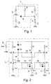
- a control unit 1 (FIG. 1) is with an operating voltage source 2 connected, in the present case the battery one Motor vehicle.
- a load resistor in the form of a sensor 3 lies between an output 4 of the circuit arrangement and a ground connection labeled GND.
- a first current source 6 is connected to the collector as Emitter follower connected transistor 7 connected. This Current source 6 may limit a short circuit current via sensor 3 to ground. The voltage drop across the base-emitter path of the transistor 7 is a diode 8 compensated. The diode 8 is located between a second current source 9 and a reference voltage source 10. The of the Operating voltage source 2 supplied operating voltage Vbat (see FIG. 2) of the circuit arrangement 1 must be larger than that reference voltage supplied by the reference voltage source 10 (Vref) be. The second current source 9 drives a constant Current through the diode 8 and thus prevents one Passage of the operating voltage to the supply voltage for the sensor 3.
- the reference voltage is from the emitter follower transistor 7 buffered to the sensor 3 acting as a load resistor posed.
- “buffered” means that the reference voltage source 10 no electricity is drawn and that it consequently is not burdened by the load resistance.
- control unit 1 Other components of the control unit 1 are not shown here described, since it does not affect the invention and on the other hand in various versions in general are known and described in many publications.
- Two transistors Q3 and Q4, which - as can be seen from the drawing - Are connected as emitter followers the transistor 7 of Figure 1.
- Their base is in each case a resistor R7 or R6 to a further transistor Q6 connected by connecting its base to its Collector is connected as a diode and the diode 8 of Figure 1 corresponds.
- the connected to a load resistor RL1 or RL2 Emitters of transistors Q3 and Q4 each form an output 4 or 5 of the circuit arrangement, on each of which identical to the reference voltage Vref of the control unit Voltage short-circuit proof as supply or operating voltage is provided for the sensors 3.
Landscapes
- Engineering & Computer Science (AREA)
- Physics & Mathematics (AREA)
- Electromagnetism (AREA)
- General Physics & Mathematics (AREA)
- Radar, Positioning & Navigation (AREA)
- Automation & Control Theory (AREA)
- Continuous-Control Power Sources That Use Transistors (AREA)
- Control Of Voltage And Current In General (AREA)
Description
- Figur 1
- ein mit einer erfindungsgemäßen Schaltungsanordnung versehenes Steuergerät als Prinzipschaltbild, und
- Figur 2
- einen Schaltplan der Schaltungsanordnung nach Figur 1.
Claims (5)
- Schaltungsanordnung zum Versorgen von elektrischen Verbrauchern (3), insbesondere von Sensoren in einem Kraftfahrzeug, mit einer für ihren Betrieb erforderlichen konstanten Spannung (Vref), die aus einer Betriebsspannungsquelle (2) erzeugt wird,
dadurch gekennzeichnet,
daß wenigstens eine erste Reihenschaltung, bestehend aus einer ersten Stromquelle (6, Q1), einem als Emitterfolger geschalteten Transistor (7, Q3) und einem Verbraucher (3), und eine zweite Reihenschaltung, bestehend aus einer zweiten Stromquelle (9, Q5), einer Diode (8, Q6) und einer Referenzspannungsquelle (10), jeweils parallel zur Betriebsspannungsquelle (2) angeordnet sind, und daß die Basis des Transistors (7, Q3) mit der Anode der Diode (8, Q6) verbunden ist. - Schaltungsanordnung nach Anspruch 1, dadurch gekennzeichnet, daß die erste Stromquelle (6) einen Transistor (Q1, Q2) enthält, dessen Emitter über einen Widerstand (R1, R2) mit dem Pluspol der Betriebsspannungsquelle (2), dessen Kollektor mit dem Kollektor des Transistors (7, Q3, Q4), und dessen Basis über einen Widerstand (R4, R5) mit dem Abgriff eines parallel zur Betriebsspannungsquelle (2) liegenden Spannungsteilers (D1, D2, R8) verbunden ist.
- Schaltungsanordnung nach Anspruch 1, dadurch gekennzeichnet, daß die Diode (8) ein als Diode geschalteter Transistor (Q6) ist.
- Schaltungsanordnung nach Anspruch 1 oder 2, dadurch gekennzeichnet, daß die zweite Stromquelle (9) einen Transistor (Q5) enthält, dessen Emitter über einen Widerstand (R3) mit dem Pluspol der Betriebsspannungsquelle (2), dessen Kollektor mit der Anode der Diode (8, Q6) und dessen Basis mit dem Abgriff des Spannungsteilers (D1, D2, R8) verbunden ist.
- Schaltungsanordnung nach einem der vorhergehenden Ansprüche, dadurch gekennzeichnet, daß der Transistor (7, Q3, Q4) als Emitterfolger mit einer Diode (D3, D4) in Durchlaßrichtung vom Emitter zur Basis beschaltet ist, dessen Basis über einen Widerstand (R7, R6) mit der Anode der Diode (8, Q6) verbunden ist, und zwischen dessen Emitter, an dem die konstante Spannung (Vref) zur Verfügung steht, und dem Minuspol (GND) der Betriebsspannungsquelle (2) der Verbraucher (3) angeordnet ist.
Priority Applications (3)
| Application Number | Priority Date | Filing Date | Title |
|---|---|---|---|
| EP93115240A EP0645686B1 (de) | 1993-09-21 | 1993-09-21 | Schaltungsanordnung zum Versorgen von elektrischen Verbrauchern mit einer konstanten Spannung |
| DE59309986T DE59309986D1 (de) | 1993-09-21 | 1993-09-21 | Schaltungsanordnung zum Versorgen von elektrischen Verbrauchern mit einer konstanten Spannung |
| US08/309,953 US5592075A (en) | 1993-09-21 | 1994-09-21 | Circuit configuration for supplying electrical consumers with a constant voltage |
Applications Claiming Priority (1)
| Application Number | Priority Date | Filing Date | Title |
|---|---|---|---|
| EP93115240A EP0645686B1 (de) | 1993-09-21 | 1993-09-21 | Schaltungsanordnung zum Versorgen von elektrischen Verbrauchern mit einer konstanten Spannung |
Publications (2)
| Publication Number | Publication Date |
|---|---|
| EP0645686A1 EP0645686A1 (de) | 1995-03-29 |
| EP0645686B1 true EP0645686B1 (de) | 2000-03-22 |
Family
ID=8213290
Family Applications (1)
| Application Number | Title | Priority Date | Filing Date |
|---|---|---|---|
| EP93115240A Expired - Lifetime EP0645686B1 (de) | 1993-09-21 | 1993-09-21 | Schaltungsanordnung zum Versorgen von elektrischen Verbrauchern mit einer konstanten Spannung |
Country Status (3)
| Country | Link |
|---|---|
| US (1) | US5592075A (de) |
| EP (1) | EP0645686B1 (de) |
| DE (1) | DE59309986D1 (de) |
Families Citing this family (2)
| Publication number | Priority date | Publication date | Assignee | Title |
|---|---|---|---|---|
| DE19750049A1 (de) * | 1997-11-12 | 1999-05-20 | Bosch Gmbh Robert | Sensoranordnung bestehend aus Sensor und Auswerteschaltung |
| US9831764B2 (en) * | 2014-11-20 | 2017-11-28 | Stmicroelectronics International N.V. | Scalable protection voltage generator |
Family Cites Families (9)
| Publication number | Priority date | Publication date | Assignee | Title |
|---|---|---|---|---|
| FR2412850A1 (fr) * | 1977-04-26 | 1979-07-20 | Suwa Seikosha Kk | Circuit integre a semi-conducteurs |
| JPS58144920A (ja) * | 1982-02-23 | 1983-08-29 | Toshiba Corp | 定電流回路 |
| DE3342735A1 (de) * | 1982-11-26 | 1984-05-30 | Tokyo Shibaura Denki K.K., Kawasaki, Kanagawa | Impedanzwandlerschaltung |
| US4736125A (en) * | 1986-08-28 | 1988-04-05 | Applied Micro Circuits Corporation | Unbuffered TTL-to-ECL translator with temperature-compensated threshold voltage obtained from a constant-current reference voltage |
| US4740766A (en) * | 1987-09-04 | 1988-04-26 | Tektronix, Inc. | Precision tracking current generator |
| AT398865B (de) * | 1990-09-19 | 1995-02-27 | E Z I Entwicklungszentrum Fuer | Strombegrenzungsschaltung |
| DE4114073C3 (de) * | 1991-04-30 | 2001-07-05 | Bosch Gmbh Robert | Schaltungsanordnung zur Stabilisierung einer Spannung |
| JPH0535350A (ja) * | 1991-07-26 | 1993-02-12 | Nec Yamagata Ltd | 定電流源 |
| US5373253A (en) * | 1993-09-20 | 1994-12-13 | International Business Machines Corporation | Monolithic current mirror circuit employing voltage feedback for β-independent dynamic range |
-
1993
- 1993-09-21 DE DE59309986T patent/DE59309986D1/de not_active Expired - Fee Related
- 1993-09-21 EP EP93115240A patent/EP0645686B1/de not_active Expired - Lifetime
-
1994
- 1994-09-21 US US08/309,953 patent/US5592075A/en not_active Expired - Lifetime
Also Published As
| Publication number | Publication date |
|---|---|
| DE59309986D1 (de) | 2000-04-27 |
| US5592075A (en) | 1997-01-07 |
| EP0645686A1 (de) | 1995-03-29 |
Similar Documents
| Publication | Publication Date | Title |
|---|---|---|
| EP0107028A2 (de) | Schaltungsanordnung mit einer Ausgangstransistorschaltung und einer Schutzschaltung zur Begrenzung des Ausgangsstroms der Ausgangstransistorschaltung | |
| DE3402891A1 (de) | Spannungs-stromkonverter hoher genauigkeit, insbesondere fuer niedrige versorgungsspannungen | |
| DE69200655T2 (de) | Schaltung zur Regelung der Ladespannung einer mittels eines Generators gespeisten Batterie. | |
| EP0645686B1 (de) | Schaltungsanordnung zum Versorgen von elektrischen Verbrauchern mit einer konstanten Spannung | |
| DE2045768B2 (de) | Regeleinrichtung für einen Wechselstromgenerator | |
| DE3607966A1 (de) | Schaltungsanordnung zur spannungsregelung, insbesondere fuer wechselstromgeneratoren | |
| EP0814396A2 (de) | Schaltungsanordnung zur Erzeugung eines Referenzpotentials | |
| DE3447002A1 (de) | Konstantstromgeneratorschaltkreis | |
| EP0698794A1 (de) | Schaltungsanordnung zur Unterspannungs-Erkennung | |
| DE102018217496A1 (de) | Startschaltung | |
| DE10314842A1 (de) | Stromerfassungsschaltung für einen DC/DC-Wandler | |
| DE3329664C2 (de) | ||
| DE3832378C1 (de) | ||
| DE3115051C2 (de) | Spannungs/Strom-Wandlerschaltung | |
| DE3147562A1 (de) | "schaltung mit veraenderbarer impedanz" | |
| EP0682305B1 (de) | Schaltungsanordnung zur Erzeugung eines Referenzstroms | |
| DE2541545A1 (de) | Rutschschutzsystem fuer fahrzeugraeder | |
| DE3643869C1 (de) | Schaltungsanordnung zur UEberwachung einer Brueckenendstufe | |
| DE3939408C2 (de) | ||
| EP0552471A1 (de) | Schutzschaltung für elektronische Schaltungen | |
| DE3611548A1 (de) | Stromspiegelschaltung | |
| DE3806058C2 (de) | ||
| EP0309451B1 (de) | Schutzvorrichtung gegen störsignale | |
| DE102008044464B4 (de) | Vorrichtung zur Auswertung eines Strommesssignals | |
| DE19535807C1 (de) | Schaltungsanordnung zur Erzeugung eines Biaspotentials |
Legal Events
| Date | Code | Title | Description |
|---|---|---|---|
| PUAI | Public reference made under article 153(3) epc to a published international application that has entered the european phase |
Free format text: ORIGINAL CODE: 0009012 |
|
| AK | Designated contracting states |
Kind code of ref document: A1 Designated state(s): DE FR GB |
|
| 17P | Request for examination filed |
Effective date: 19950424 |
|
| 17Q | First examination report despatched |
Effective date: 19950626 |
|
| GRAG | Despatch of communication of intention to grant |
Free format text: ORIGINAL CODE: EPIDOS AGRA |
|
| GRAG | Despatch of communication of intention to grant |
Free format text: ORIGINAL CODE: EPIDOS AGRA |
|
| GRAH | Despatch of communication of intention to grant a patent |
Free format text: ORIGINAL CODE: EPIDOS IGRA |
|
| GRAH | Despatch of communication of intention to grant a patent |
Free format text: ORIGINAL CODE: EPIDOS IGRA |
|
| GRAA | (expected) grant |
Free format text: ORIGINAL CODE: 0009210 |
|
| AK | Designated contracting states |
Kind code of ref document: B1 Designated state(s): DE FR GB |
|
| GBT | Gb: translation of ep patent filed (gb section 77(6)(a)/1977) |
Effective date: 20000324 |
|
| REF | Corresponds to: |
Ref document number: 59309986 Country of ref document: DE Date of ref document: 20000427 |
|
| ET | Fr: translation filed | ||
| PLBE | No opposition filed within time limit |
Free format text: ORIGINAL CODE: 0009261 |
|
| STAA | Information on the status of an ep patent application or granted ep patent |
Free format text: STATUS: NO OPPOSITION FILED WITHIN TIME LIMIT |
|
| 26N | No opposition filed | ||
| REG | Reference to a national code |
Ref country code: GB Ref legal event code: IF02 |
|
| PGFP | Annual fee paid to national office [announced via postgrant information from national office to epo] |
Ref country code: GB Payment date: 20030904 Year of fee payment: 11 |
|
| PG25 | Lapsed in a contracting state [announced via postgrant information from national office to epo] |
Ref country code: GB Free format text: LAPSE BECAUSE OF NON-PAYMENT OF DUE FEES Effective date: 20040921 |
|
| GBPC | Gb: european patent ceased through non-payment of renewal fee |
Effective date: 20040921 |
|
| PGFP | Annual fee paid to national office [announced via postgrant information from national office to epo] |
Ref country code: FR Payment date: 20050912 Year of fee payment: 13 |
|
| PGFP | Annual fee paid to national office [announced via postgrant information from national office to epo] |
Ref country code: DE Payment date: 20051121 Year of fee payment: 13 |
|
| PG25 | Lapsed in a contracting state [announced via postgrant information from national office to epo] |
Ref country code: DE Free format text: LAPSE BECAUSE OF NON-PAYMENT OF DUE FEES Effective date: 20070403 |
|
| REG | Reference to a national code |
Ref country code: FR Ref legal event code: ST Effective date: 20070531 |
|
| PG25 | Lapsed in a contracting state [announced via postgrant information from national office to epo] |
Ref country code: FR Free format text: LAPSE BECAUSE OF NON-PAYMENT OF DUE FEES Effective date: 20061002 |