EP0644641A2 - Garnitur zum Verbinden eines Energiekabels und damit ausgerüstetes Energiekabel - Google Patents
Garnitur zum Verbinden eines Energiekabels und damit ausgerüstetes Energiekabel Download PDFInfo
- Publication number
- EP0644641A2 EP0644641A2 EP94402054A EP94402054A EP0644641A2 EP 0644641 A2 EP0644641 A2 EP 0644641A2 EP 94402054 A EP94402054 A EP 94402054A EP 94402054 A EP94402054 A EP 94402054A EP 0644641 A2 EP0644641 A2 EP 0644641A2
- Authority
- EP
- European Patent Office
- Prior art keywords
- cable
- equipment
- external
- stripped
- semiconductor screen
- Prior art date
- Legal status (The legal status is an assumption and is not a legal conclusion. Google has not performed a legal analysis and makes no representation as to the accuracy of the status listed.)
- Granted
Links
Images
Classifications
-
- H—ELECTRICITY
- H01—ELECTRIC ELEMENTS
- H01B—CABLES; CONDUCTORS; INSULATORS; SELECTION OF MATERIALS FOR THEIR CONDUCTIVE, INSULATING OR DIELECTRIC PROPERTIES
- H01B9/00—Power cables
-
- H—ELECTRICITY
- H02—GENERATION; CONVERSION OR DISTRIBUTION OF ELECTRIC POWER
- H02G—INSTALLATION OF ELECTRIC CABLES OR LINES, OR OF COMBINED OPTICAL AND ELECTRIC CABLES OR LINES
- H02G15/00—Cable fittings
- H02G15/08—Cable junctions
- H02G15/18—Cable junctions protected by sleeves, e.g. for communication cable
- H02G15/184—Cable junctions protected by sleeves, e.g. for communication cable with devices for relieving electrical stress
-
- H—ELECTRICITY
- H02—GENERATION; CONVERSION OR DISTRIBUTION OF ELECTRIC POWER
- H02G—INSTALLATION OF ELECTRIC CABLES OR LINES, OR OF COMBINED OPTICAL AND ELECTRIC CABLES OR LINES
- H02G15/00—Cable fittings
- H02G15/08—Cable junctions
- H02G15/10—Cable junctions protected by boxes, e.g. by distribution, connection or junction boxes
- H02G15/103—Cable junctions protected by boxes, e.g. by distribution, connection or junction boxes with devices for relieving electrical stress
Definitions
- the present invention relates to medium, high or very high voltage energy cables for use in direct or alternating current. It relates more particularly to accessory equipment for connecting such a cable and to the energy cable thus equipped.
- the power cables include a conductive core, an internal semiconductor screen covering the core, a dielectric insulation layer on the internal semiconductor screen, an external semiconductor screen on the dielectric layer and a sheath of external protection.
- the insulating dielectric layer is in particular a tape or extruded polymeric insulator.
- the protective sheath can be metallic, in particular lead for buried energy cables, and then also play the role of metallic metallic screen, or can be insulating and then generally associated with an underlying metallic screen of mass.
- the semiconductor screens are made for example of a polymeric material containing carbon black.
- connection equipment mounted on the power cables are in particular terminations for connection to the network or to an apparatus, branches between cables or connection in branch of an apparatus, or even junctions of two cables.
- the layers of the terminal part of the cable are stripped in gradation, for access to each of them and to the core and the mounting of the connection piece and of the associated accessory equipment.
- the accessory equipment must also ensure dielectric strength, in particular when the internal and external semiconductor screens of the cable are stopped.
- they can be made mainly of insulating material (in the form of a tape or a sleeve), and wear or be mounted on a semiconductor layer provided in suitable places to ensure the reconstruction of the semi screen - internal conductor.
- insulating material in the form of a tape or a sleeve
- the semiconductor layer provided in suitable places to ensure the reconstruction of the semi screen - internal conductor.
- the reconstitution of the external semiconductor screen they are covered, once mounted on the cable, with a suitable semiconductor layer.
- the accessory connection equipment is preferably formed, in a widely known manner, by a single insulating sleeve whose internal face is semiconductor over at least part of the length of the sleeve.
- a sleeve covers at least the stripped parts of the internal semiconductor screen and of the dielectric layer. It is relatively rigid and then of internal section adapted to the sections of the parts to be covered, or is retractable on these parts to be covered.
- the continuity of the external semiconductor screen is ensured by recovery, for example by tape of a semiconductor layer covering the sleeve and extending to the external semiconductor screen of the cable.
- Such a rigid or retractable sleeve must ensure uniform radial contact between the internal and external semiconductor screens and the corresponding semiconductor parts of its internal and external faces, for a homogeneous distribution of the electric field.
- the end portion of the sleeve, around the outer semiconductor screen is often semiconductor throughout its thickness made relatively reduced, and the semiconductor outer face starts from this semiconductor end portion in having a conical shape, to form a deflector integrated into the sleeve and thus ensure the homogeneous distribution of the electric field at the stop of the external semiconductor screen of the cable.
- the object of the present invention is to avoid these drawbacks, by simplifying the obtaining of the functions provided by the accessory connection equipment and by reducing the time and the difficulties for their correct installation. It also aims to improve the dielectric strength obtained.
- the present invention provides for this purpose an accessory power cable connection equipment, intended to be mounted on a stripped end portion of said cable and to ensure the dielectric strength around said stripped end portion, said cable comprising a conductive core and successively , around said core, an internal semiconductor screen, a dielectric layer, an external semiconductor screen and a protective sheath exterior and said accessory equipment comprising a first part intended to ensure the reconstruction of said dielectric layer, a second and a third associated parts intended to ensure the reconstruction of said internal semiconductor screen and said external semiconductor screen respectively, characterized in that said first and second parts of said accessory connection equipment are produced identically and simultaneously in an insulating polymer matrix containing at least one conductive polymer, incorporated into said polymer matrix with a mass rate such that the resulting electrical conductivity of said first and second parts is less than 10 ⁇ 14 S / cm for use in direct current and less than 10 ⁇ 10 S / cm for use in alternating current, and in that said third part has an electrical conductivity less than 1 S / cm.
- the accessory connection equipment according to the invention has only two separate parts, which simplifies its production and its installation.
- the electrical conductivity of the latter varies locally depending on the electric field, so that, in the vicinity of the internal semiconductor screen of the cable, the he equipment behaves like a semiconductor screen, and in the vicinity of the dielectric cable insulation layer, the equipment behaves substantially like an insulator.
- the equipment according to the invention makes it possible to avoid complete stripping of the cable; it suffices to expose the conductive core and the external semiconductor screen, by making a straight cut (or possibly bias) of the different layers between these two parts.
- the insulating polymer matrix incorporates at most 20% by mass of a conductive polymer chosen from undoped and dedoped polymers; when the conductive polymer used is a self-doped conductive polymer, its mass content in the polymer matrix is at most 5%.
- the invention also relates to an energy cable, equipped with such equipment, characterized in that said end portion of said cable is stripped continuously through simultaneously at least said external semiconductor screen, said dielectric layer and said internal semiconductor screen, up to said core, and carries said interior section equipment adapted to said terminal part thus stripped.
- this cable connected by a connection element to another energy cable with also stripped end part is characterized in that said equipment is molded directly on said connection element and on either side on the stripped end portions of said cables.
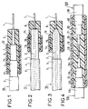
- each energy cable shown is identical from one figure to another and are designated by the same reference numbers, these reference numbers being simply accompanied by the additional letter A or B in FIG. 4.
- the cable (s) are themselves designated under the global reference 10, accompanied by the letter A for one of the cables and the letter B for the other, in FIG. 4.
- Each cable comprises a conductive core 1 and successively an internal semiconductor screen 2, a dielectric insulation layer 3, an external semiconductor screen 4 and an external protective sheath 5.
- This protective sheath is metallic and in particular made of lead. or a lead alloy, or can be insulating and is then generally associated with a directly underlying metal screen, not shown.
- FIG. 1 it can be seen that the constituent parts of the cable 10 have been stripped successively in gradation on the terminal part of the cable and that this terminal part thus prepared carries an adapter 7 according to the invention, also called reducer, surrounding the screen stripped external semiconductor 4 in part, the stripped dielectric layer 3 and the stripped internal semiconductor screen 2.
- an adapter 7 also called reducer
- the adapter 7 is a semiconductor layer 11 used to ensure the reconstitution of the stripped external semiconductor screen 4 as well as the dielectric strength at the level thereof, and extending for this purpose up to to him by partially surrounding him.
- the assembly comprising the adapter 7 and the semiconductor layer 11 constitutes an accessory connection equipment 12 according to the invention.
- the adapter 7 is made, according to the invention, of a material constituted by an insulating polymer matrix containing a dedoped or undoped conductive polymer, incorporated with a rate which is at most 20% by mass in the matrix.
- the adapter 7 is made of a material consisting of an insulating polymer matrix containing a self-doping conductive polymer, incorporated with a content at most equal to 5% by mass in the matrix.
- the semiconductor layer 11 has conductivity less than 1 S / cm, both in direct current and in alternating current, and can be made for example of a material of the type described in document EP-A-0 507 676 , that is to say be constituted by an insulating polymer matrix which contains a dedoped or undoped conductive polymer incorporated in the matrix with a content of 5 to 70% by mass, preferably of 20 to 30%, or else a self-doping conductive polymer, incorporated into the matrix at a rate greater than 5%, and preferably from 10 to 40%.
- the layer 11 can also be made of a usual semiconductor material.
- the adapter 7 forms a sleeve covering the stripped parts of the external semiconductor screen 4 (in part), of the dielectric layer 3 and of the internal semiconductor screen 2. It is directly molded on these only parts to cover, or is pre-molded and positioned on these parts then optionally then mechanically secured at the end, in particular by heating the corresponding end of the sleeve in place and / or that of the external semiconductor screen 4. It has a bore central 17 whose length and stepped section correspond to the respective lengths and the respective sections of the parts which it covers.
- the adapter 7 can be formed from an extruded strip, having the same composition as the aforementioned sleeve, which is wound around the parts to be covered and is mechanically secured to them.
- the end part of the cable 10 is prepared by a cross section of the internal semiconductor screen 2, the dielectric layer 3 and the external semiconductor screen 4 around the core 1, the outer sheath protective cover 5 being partly removed to strip part of the external semiconductor screen 4.
- the terminal part thus prepared carries an adapter 8 according to the invention, covered with a semiconductor layer 13 identical to layer 11, the adapter 8 and the layer 13 forming an accessory connection device 14 according to the invention.
- the adapter 8 is of the same composition as the adapter 7 of FIG. 1. It covers over a short length the stripped core, as well as the stripped external semiconductor screen 4. It constitutes a sleeve which is directly molded in place or is pre-molded, positioned in place on the prepared terminal part of the cable 10 and is advantageously made adherent on the straight section of cut for a good contact of the sleeve on this one.
- the bore 18 of the adapter 8 has a single shoulder at a right angle. Its section on either side of this shoulder corresponds to the respective sections of the external semiconductor screen 4 and of the core 1.
- the semiconductor layer 13 partially covers the adapter 8 and extends to the external semiconductor screen 4 by partially covering it.
- the end part of the cable 10 is prepared, not by a straight cut as in FIG. 2 but by a continuous bias cut of the external semiconductor screen 4 and of the dielectric layer 3 and a straight cut, to below, of the internal semiconductor screen 2, for exposing the core 1.
- It carries an adapter 9 according to the invention, similar to the adapter 8, the bore 19 of which has terminal portions opposite, the respective sections of which correspond to those of the external semiconductor screen 4 and of the core 1, respectively, but an intermediate frustoconical shoulder corresponding to the bias strip for stripping the core 1.
- This stripping bias cut allows better contact of the adapter 9 as well as better adhesion to the frustoconical section of the cut.
- the adapter 9 is covered with a semiconductor layer 15 identical to the semiconductor layer 13 and which extends to the external semiconductor screen 4 by partially covering it.
- the adapter 9 and the layer 15 form an accessory connection equipment 16 according to the invention.
- connection element 20 connects the ends of the exposed cores 1A and 1B.
- a sleeve or adapter 21 according to the invention is molded on the connection element 20 and on either side on the stripped parts and the terminal portions of the semiconductor screens 4A and 4B of the two cables 10A and 10B . It strengthens the mechanical strength of the connection of the cores 1A and 1B, so that the connection element 20 can be constituted by a connection piece for mechanical and electrical connection or can be constituted by a simple weld of electrical connection but of relatively low mechanical strength.
- the sleeve 21 is covered with a semiconductor layer 22 which extends on the semiconductor screens 4A and 4B and thus ensures their continuity.
- the sleeve 21 molded directly in place can be replaced by a tape of the same composition placed on the parts to be covered.
- junction may further comprise, in a known manner and not shown, a heat sink, mounted around the connection piece and extending on either side of the latter on the stripped cores, as well as two reducers , mounted on one side and the other of the dissipator on the stripped dielectric layers 3A and 3B of the two cables.
- a heat sink mounted around the connection piece and extending on either side of the latter on the stripped cores, as well as two reducers , mounted on one side and the other of the dissipator on the stripped dielectric layers 3A and 3B of the two cables.
- the sleeve 21 simultaneously performs the functions of such a heat sink and of the two reducers in this junction, thus rendered unnecessary in the junction.
- composition of the accessory connection equipment according to the invention and its main function resulting from this composition are specified below.
- the insulating polymer matrix and the conductive polymer of this accessory equipment consist of polymers which are identical to those used in the production of the semiconductor screen described in document EP-A-0 507 676.
- the polymer matrix of the accessory equipment comprises at least one thermoplastic polymer, chosen from acrylic resins, vinyl styrenics and cellulosics, polyolefins, fluorinated polymers, polyethers, polyimides, polycarbonates, polyurethanes, their silicones. copolymers, and mixtures between homopolymers and between homopolymers and copolymers.
- thermoplastic polymer is chosen from polypropylene (PP), polyethylene (PE), the copolymer of ethylene and vinyl acetate (EVA), ethylene-proprylene-diene-monomer (EPDM), fluorinated polyvinylidene (PVDF), ethylene-butylacrylate (EBA), alone or as a mixture.
- PP polypropylene
- PE polyethylene
- EVA ethylene-proprylene-diene-monomer
- PVDF fluorinated polyvinylidene
- EBA ethylene-butylacrylate
- this polymer matrix comprises at least one thermosetting polymer chosen from polyesters, epoxy resins and phenolic resins.
- the undoped or doped and then dedoped conductive polymer (s) incorporated in this polymer matrix are chosen from the group comprising polyaniline, polythiophene, polypyrrole, polyacetylene, polyparaphenylene, polyalkyltiophenes, their derivatives and their mixtures.
- undoped and dedoped polymers do not contain ionic groups.
- Their intrinsic electrical conductivity, measured in direct current, is very low and of the order of 10 ⁇ 10 to 10 ⁇ 9 S / cm.
- the conductivity of the accessory equipment, constituted by this polymer matrix containing at most 20% by mass of undoped or dedoped polymer, is of the order of 10 ⁇ 14 S / cm at low electric fields for use in direct current, and 10 ⁇ 10 S / cm at low electric fields for use in alternating current. It can be locally of the order of 10 ⁇ 9 S / cm at the high electric fields to be distributed.
- self-doped polymers When self-doped polymers are incorporated into the matrix, the latter are chosen from the group comprising autodoped polyanilines having benzene or benzene and quinone nuclei, which carry grafts consisting for the one of a hydrocarbon radical, comprising from 2 to 8 carbon atoms and interrupted by at least one hetero atom, and for the others by a strong acid function or one of its salts, said hetero atom being itself chosen from O and S and the strong acid function from the residues of sulfonic, phosphonic and phosphoric acids or their salts.
- autodoped polyanilines having benzene or benzene and quinone nuclei which carry grafts consisting for the one of a hydrocarbon radical, comprising from 2 to 8 carbon atoms and interrupted by at least one hetero atom, and for the others by a strong acid function or one of its salts, said hetero atom being itself chosen from O and S and the strong acid function from the residues of
- the intrinsic electrical conductivity, measured in direct current, of these self-doped polymers is on the order of 10 ⁇ 3 to 10 ⁇ 2 S / cm on average. It is also adjustable as desired between 10 ⁇ 5 and 1 S / cm, by varying the molecular ratio of the two types of grafts.
- the electrical conductivity of the accessory equipment, consisting of the above polymer matrix to which is added at most 5% by mass of this self-doped polymer, is itself adjustable and of the order or less than 10 ⁇ 14 S / cm for use at low electric fields in direct current, and of the order or less than 10 ⁇ 10 S / cm for use in alternating current at low electric fields.
- Such accessory accessory equipment in this composition is basically dielectric, except locally if necessary when it is subjected to a high electric field and then becomes substantially conductive to play the role of integrated deflector which is moreover adapted to the existing electric field as well. distributed.
- the accessory equipment according to the invention can be produced by a conventional process, with the possible addition of mineral fillers, stabilizers, crosslinking agents, etc. to the various materials used.
- the semiconductor layers used to ensure the reconstitution of the external semiconductor screens can be made of any usual semiconductor material.
- an external protective envelope there may be, in the usual manner, an external protective envelope.
Landscapes
- Cable Accessories (AREA)
- Processing Of Terminals (AREA)
- Coupling Device And Connection With Printed Circuit (AREA)
Applications Claiming Priority (2)
| Application Number | Priority Date | Filing Date | Title |
|---|---|---|---|
| FR9311118A FR2710204B1 (fr) | 1993-09-17 | 1993-09-17 | Equipement accessoire de raccordement d'un câble d'énergie et câble d'énergie ainsi équipé. |
| FR9311118 | 1993-09-17 |
Publications (3)
| Publication Number | Publication Date |
|---|---|
| EP0644641A2 true EP0644641A2 (de) | 1995-03-22 |
| EP0644641A3 EP0644641A3 (de) | 1997-09-17 |
| EP0644641B1 EP0644641B1 (de) | 1999-11-24 |
Family
ID=9450989
Family Applications (1)
| Application Number | Title | Priority Date | Filing Date |
|---|---|---|---|
| EP94402054A Expired - Lifetime EP0644641B1 (de) | 1993-09-17 | 1994-09-14 | Garnitur zum Verbinden eines Energiekabels und damit ausgerüstetes Energiekabel |
Country Status (9)
| Country | Link |
|---|---|
| EP (1) | EP0644641B1 (de) |
| JP (1) | JPH07170624A (de) |
| KR (1) | KR950009754A (de) |
| CN (1) | CN1113045A (de) |
| AU (1) | AU683680B2 (de) |
| DE (1) | DE69421781T2 (de) |
| DK (1) | DK0644641T3 (de) |
| FR (1) | FR2710204B1 (de) |
| NO (1) | NO943427L (de) |
Cited By (1)
| Publication number | Priority date | Publication date | Assignee | Title |
|---|---|---|---|---|
| EP0886340A1 (de) * | 1997-06-16 | 1998-12-23 | Alcatel | Kabelverbindung |
Families Citing this family (8)
| Publication number | Priority date | Publication date | Assignee | Title |
|---|---|---|---|---|
| SE525492C2 (sv) * | 2002-10-22 | 2005-03-01 | Abb Research Ltd | Fältstyrande polymermatris försedd med fyllning |
| EP2639264A1 (de) * | 2012-03-14 | 2013-09-18 | Nexans | Feldabstufungsmaterial |
| CN103595010B (zh) * | 2013-12-03 | 2016-09-07 | 深圳市沃尔核材股份有限公司 | 一种非等径物体的绝缘密封方法 |
| CN103595012B (zh) * | 2013-12-03 | 2016-09-07 | 深圳市沃尔核材股份有限公司 | 一种非等径物体的绝缘密封方法 |
| US10903639B2 (en) * | 2016-09-19 | 2021-01-26 | Prysmian S.P.A. | Joint for high voltage direct current cables |
| DE102018116399A1 (de) * | 2018-07-06 | 2020-01-09 | Nkt Gmbh & Co. Kg | Verbindungsmuffe |
| US11276971B2 (en) | 2019-05-31 | 2022-03-15 | Aptiv Technologies Limited | Hermaphroditic cable connectors for autonomous vehicles |
| EP3745425B1 (de) * | 2019-05-31 | 2022-12-21 | Aptiv Technologies Limited | Kommunikationskabel für autonome fahrzeuge |
Family Cites Families (3)
| Publication number | Priority date | Publication date | Assignee | Title |
|---|---|---|---|---|
| GB2111769B (en) * | 1978-09-14 | 1983-11-02 | Raychem Ltd | Enclosure for cable termination or joint |
| US4822952A (en) * | 1985-08-21 | 1989-04-18 | Cable Technology Laboratories, Inc. | Electrical cable joint and electrical cable termination and methods of making same |
| ES2086680T3 (es) * | 1991-04-02 | 1996-07-01 | Alcatel Cable | Material para pantalla semiconductora. |
-
1993
- 1993-09-17 FR FR9311118A patent/FR2710204B1/fr not_active Expired - Fee Related
-
1994
- 1994-09-14 EP EP94402054A patent/EP0644641B1/de not_active Expired - Lifetime
- 1994-09-14 AU AU72966/94A patent/AU683680B2/en not_active Ceased
- 1994-09-14 DE DE69421781T patent/DE69421781T2/de not_active Expired - Fee Related
- 1994-09-14 DK DK94402054T patent/DK0644641T3/da active
- 1994-09-15 NO NO943427A patent/NO943427L/no not_active Application Discontinuation
- 1994-09-16 KR KR1019940023608A patent/KR950009754A/ko not_active Ceased
- 1994-09-16 CN CN94115386A patent/CN1113045A/zh active Pending
- 1994-09-16 JP JP6222104A patent/JPH07170624A/ja active Pending
Cited By (2)
| Publication number | Priority date | Publication date | Assignee | Title |
|---|---|---|---|---|
| EP0886340A1 (de) * | 1997-06-16 | 1998-12-23 | Alcatel | Kabelverbindung |
| US6105247A (en) * | 1997-06-16 | 2000-08-22 | Alcatel | Method of making a cable joint |
Also Published As
| Publication number | Publication date |
|---|---|
| EP0644641B1 (de) | 1999-11-24 |
| AU7296694A (en) | 1995-03-30 |
| FR2710204A1 (fr) | 1995-03-24 |
| DK0644641T3 (da) | 2000-05-22 |
| NO943427D0 (no) | 1994-09-15 |
| DE69421781T2 (de) | 2000-06-29 |
| AU683680B2 (en) | 1997-11-20 |
| FR2710204B1 (fr) | 1995-10-20 |
| NO943427L (no) | 1995-03-20 |
| JPH07170624A (ja) | 1995-07-04 |
| CN1113045A (zh) | 1995-12-06 |
| KR950009754A (ko) | 1995-04-24 |
| DE69421781D1 (de) | 1999-12-30 |
| EP0644641A3 (de) | 1997-09-17 |
Similar Documents
| Publication | Publication Date | Title |
|---|---|---|
| EP0587492B1 (de) | Rauscharmes Kabel | |
| EP0129485B1 (de) | Kabelstruktur und ihre Anwendungen | |
| EP2859633B1 (de) | Vorrichtung mit einer ladungsblockierungsschicht | |
| FR2738947A1 (fr) | Cable multipaires, blinde par paire et aise a raccorder | |
| CA2088215C (fr) | Cable electrique haute frequence | |
| CA1217249A (en) | Electrical stress control apparatus and method | |
| FR2698736A1 (fr) | Perfectionnements aux parafoudres à varistances notamment pour haute tension. | |
| EP0644641B1 (de) | Garnitur zum Verbinden eines Energiekabels und damit ausgerüstetes Energiekabel | |
| WO1997001880A1 (fr) | Jonction de cables de puissance | |
| EP2483894A1 (de) | Mittel- oder hochspannungsstromkabel | |
| FR2980622A1 (fr) | Element electrique comprenant une couche d'un materiau polymerique a gradient de conductivite electrique | |
| EP2765581A1 (de) | Elektrisches Kabel, das resistent gegen Teilentladungen ist | |
| EP0645781B1 (de) | Energiekabel mit verbesserter dielektrischen Festigkeit | |
| FR2883425A1 (fr) | Extremite synthetique de cable electrique pour tension continue | |
| EP0833421B1 (de) | Garnitur für Kabelendverschluss und Material für die Bildung der Garnitur | |
| EP3422366A1 (de) | Kabel, das ein elektrisch leitendes element umfasst, das metallisierte karbonfasern enthält | |
| EP3965123A1 (de) | Elektrisches kabel für die luftfahrtindustrie | |
| FR2601184A1 (fr) | Cable electrique de securite resistant au feu et non-propagateur de l'incendie, ainsi que son procede de fabrication | |
| FR2990047A1 (fr) | Cable de transmission electrique a haute tension | |
| EP0115322A1 (de) | Ein Ende eines elektrischen Mittelspannungskabels abdeckende gegossene Vorrichtung | |
| EP0405538A1 (de) | Wasserfestes mehrphasiges elektrisches Niederspannungsenergiekabel | |
| FR2596568A1 (fr) | Cable piezoelectrique et procede de fabrication d'un cable | |
| FR2710184A1 (fr) | Câble d'énergie à rigidité diélectrique améliorée. | |
| EP2498264B1 (de) | Mittel- oder Hochspannungsstromkabel | |
| CA1266102A (en) | Electric cables |
Legal Events
| Date | Code | Title | Description |
|---|---|---|---|
| PUAI | Public reference made under article 153(3) epc to a published international application that has entered the european phase |
Free format text: ORIGINAL CODE: 0009012 |
|
| AK | Designated contracting states |
Kind code of ref document: A2 Designated state(s): CH DE DK FR GB IT LI NL SE |
|
| PUAL | Search report despatched |
Free format text: ORIGINAL CODE: 0009013 |
|
| AK | Designated contracting states |
Kind code of ref document: A3 Designated state(s): CH DE DK FR GB IT LI NL SE |
|
| 17P | Request for examination filed |
Effective date: 19980219 |
|
| GRAG | Despatch of communication of intention to grant |
Free format text: ORIGINAL CODE: EPIDOS AGRA |
|
| 17Q | First examination report despatched |
Effective date: 19981130 |
|
| GRAG | Despatch of communication of intention to grant |
Free format text: ORIGINAL CODE: EPIDOS AGRA |
|
| GRAH | Despatch of communication of intention to grant a patent |
Free format text: ORIGINAL CODE: EPIDOS IGRA |
|
| GRAH | Despatch of communication of intention to grant a patent |
Free format text: ORIGINAL CODE: EPIDOS IGRA |
|
| RAP1 | Party data changed (applicant data changed or rights of an application transferred) |
Owner name: ALCATEL |
|
| GRAA | (expected) grant |
Free format text: ORIGINAL CODE: 0009210 |
|
| AK | Designated contracting states |
Kind code of ref document: B1 Designated state(s): CH DE DK FR GB IT LI NL SE |
|
| REG | Reference to a national code |
Ref country code: CH Ref legal event code: EP |
|
| REF | Corresponds to: |
Ref document number: 69421781 Country of ref document: DE Date of ref document: 19991230 |
|
| GBT | Gb: translation of ep patent filed (gb section 77(6)(a)/1977) |
Effective date: 19991224 |
|
| ITF | It: translation for a ep patent filed | ||
| REG | Reference to a national code |
Ref country code: DK Ref legal event code: T3 |
|
| PGFP | Annual fee paid to national office [announced via postgrant information from national office to epo] |
Ref country code: GB Payment date: 20000814 Year of fee payment: 7 |
|
| PGFP | Annual fee paid to national office [announced via postgrant information from national office to epo] |
Ref country code: CH Payment date: 20000816 Year of fee payment: 7 |
|
| PGFP | Annual fee paid to national office [announced via postgrant information from national office to epo] |
Ref country code: NL Payment date: 20000824 Year of fee payment: 7 |
|
| PGFP | Annual fee paid to national office [announced via postgrant information from national office to epo] |
Ref country code: SE Payment date: 20000825 Year of fee payment: 7 Ref country code: DK Payment date: 20000825 Year of fee payment: 7 |
|
| PGFP | Annual fee paid to national office [announced via postgrant information from national office to epo] |
Ref country code: DE Payment date: 20000830 Year of fee payment: 7 |
|
| PGFP | Annual fee paid to national office [announced via postgrant information from national office to epo] |
Ref country code: FR Payment date: 20000831 Year of fee payment: 7 |
|
| PLBE | No opposition filed within time limit |
Free format text: ORIGINAL CODE: 0009261 |
|
| STAA | Information on the status of an ep patent application or granted ep patent |
Free format text: STATUS: NO OPPOSITION FILED WITHIN TIME LIMIT |
|
| 26N | No opposition filed | ||
| REG | Reference to a national code |
Ref country code: CH Ref legal event code: PUE Owner name: ALCATEL TRANSFER- NEXANS |
|
| NLS | Nl: assignments of ep-patents |
Owner name: NEXANS |
|
| PG25 | Lapsed in a contracting state [announced via postgrant information from national office to epo] |
Ref country code: GB Free format text: LAPSE BECAUSE OF NON-PAYMENT OF DUE FEES Effective date: 20010914 Ref country code: DK Free format text: LAPSE BECAUSE OF NON-PAYMENT OF DUE FEES Effective date: 20010914 |
|
| PG25 | Lapsed in a contracting state [announced via postgrant information from national office to epo] |
Ref country code: SE Free format text: LAPSE BECAUSE OF NON-PAYMENT OF DUE FEES Effective date: 20010915 |
|
| PG25 | Lapsed in a contracting state [announced via postgrant information from national office to epo] |
Ref country code: LI Free format text: LAPSE BECAUSE OF NON-PAYMENT OF DUE FEES Effective date: 20010930 Ref country code: CH Free format text: LAPSE BECAUSE OF NON-PAYMENT OF DUE FEES Effective date: 20010930 |
|
| REG | Reference to a national code |
Ref country code: GB Ref legal event code: IF02 |
|
| PG25 | Lapsed in a contracting state [announced via postgrant information from national office to epo] |
Ref country code: NL Free format text: LAPSE BECAUSE OF NON-PAYMENT OF DUE FEES Effective date: 20020401 |
|
| GBPC | Gb: european patent ceased through non-payment of renewal fee |
Effective date: 20010914 |
|
| PG25 | Lapsed in a contracting state [announced via postgrant information from national office to epo] |
Ref country code: DE Free format text: LAPSE BECAUSE OF NON-PAYMENT OF DUE FEES Effective date: 20020501 |
|
| EUG | Se: european patent has lapsed |
Ref document number: 94402054.4 |
|
| REG | Reference to a national code |
Ref country code: CH Ref legal event code: PL |
|
| NLV4 | Nl: lapsed or anulled due to non-payment of the annual fee |
Effective date: 20020401 |
|
| REG | Reference to a national code |
Ref country code: DK Ref legal event code: EBP |
|
| NLV4 | Nl: lapsed or anulled due to non-payment of the annual fee |
Effective date: 20020401 |
|
| PG25 | Lapsed in a contracting state [announced via postgrant information from national office to epo] |
Ref country code: FR Free format text: LAPSE BECAUSE OF NON-PAYMENT OF DUE FEES Effective date: 20030603 |
|
| REG | Reference to a national code |
Ref country code: FR Ref legal event code: ST |
|
| PG25 | Lapsed in a contracting state [announced via postgrant information from national office to epo] |
Ref country code: IT Free format text: LAPSE BECAUSE OF NON-PAYMENT OF DUE FEES;WARNING: LAPSES OF ITALIAN PATENTS WITH EFFECTIVE DATE BEFORE 2007 MAY HAVE OCCURRED AT ANY TIME BEFORE 2007. THE CORRECT EFFECTIVE DATE MAY BE DIFFERENT FROM THE ONE RECORDED. Effective date: 20050914 |
|
| PG25 | Lapsed in a contracting state [announced via postgrant information from national office to epo] |
Ref country code: FR Free format text: LAPSE BECAUSE OF NON-PAYMENT OF DUE FEES Effective date: 20010930 |